

Page 1

SA621
1GHz - Low voltage LNA, mixer and VCO
Product specification 1997 Nov 07
INTEGRATED CIRCUITS
IC17 Data handbook
Page 2
Philips Semiconductors Product specification
SA6211GHz low voltage LNA, mixer and VCO
2
1997 Nov 07 853-1849 018660
DESCRIPTION
The SA621 is a combined low-noise amplifier, mixer and VCO
designed for high-performance low-power communication systems
from 800-1000MHz. The low-noise preamplifier has a 1.7dB noise
figure at 881MHz with 15dB gain and an IP3 intercept of -7dBm at
the input. The gain is stabilized by on-chip compensation to vary
less than ±0.2dB over -40 to +85°C temperature range. The
wide-dynamic-range mixer has a 12dB noise figure and IP3 of
+4.5dBm at the input at 881MHz. The integrated VCO circuit with
external resonator produces a high quality LO signal that drives the
mixer and is buffered to an external PLL synthesizer IC. The
nominal current drawn from a single 3V supply is 13.3mA.
Additionally, the entire circuit can be powered down to further reduce
the supply current to less than 20µA.
FEATURES
•Low current consumption
•Outstanding gain and noise figure
•Excellent gain stability versus temperature and supply voltage
•LNA, mixer and VCO power down capability
•Monotonic VCO frequency vs control voltage
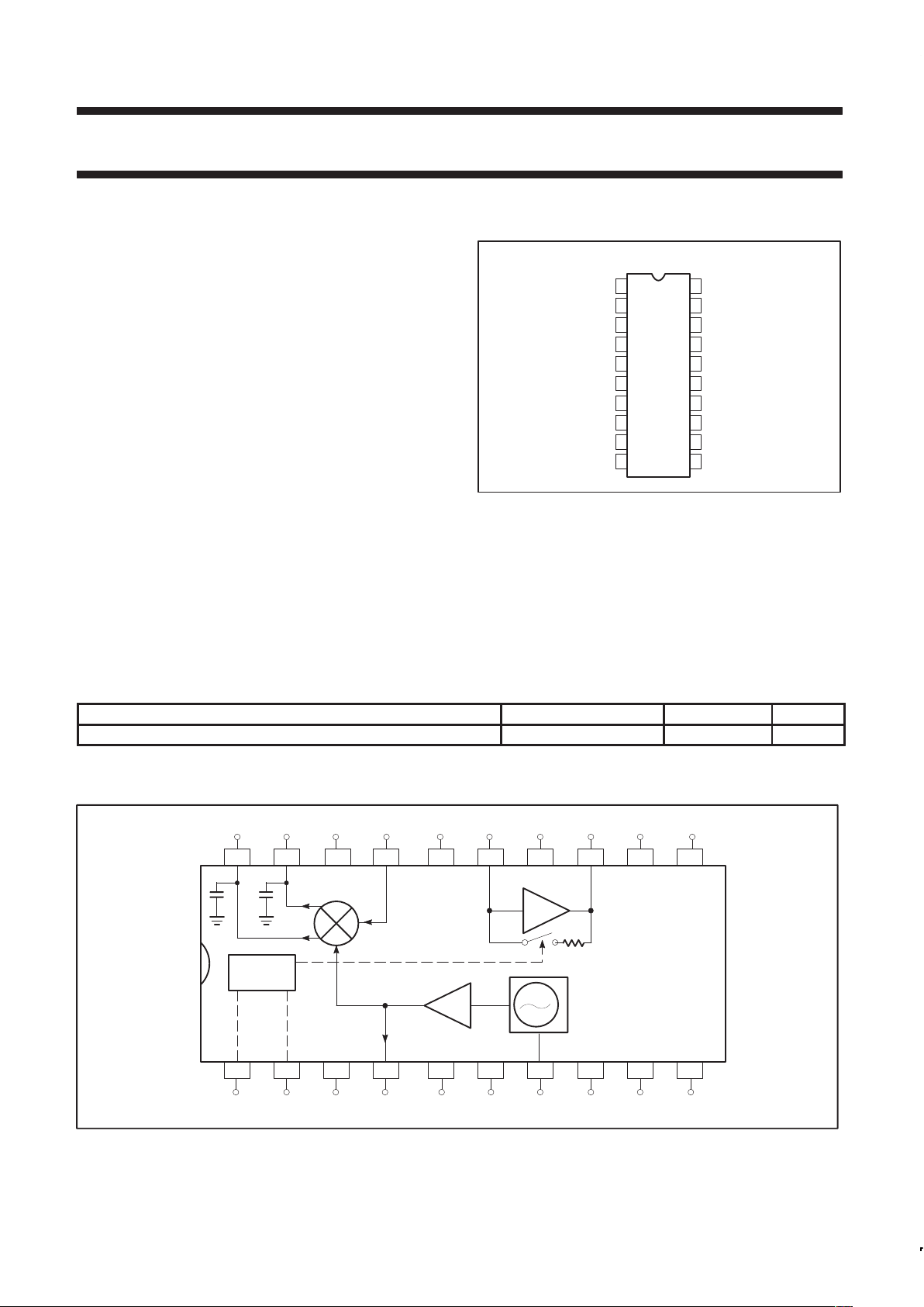
PIN CONFIGURATION
SR01429
1
2
3
4
5
6
7
8
9
10
11
12
13
14
20
19
18
17
16
15
GND
LNA OUT
V
CC
LNA IN
GND
GND
MIXER IN
MIXER OUT
MIXER OUT
GND
GND
BYPASS
GND
TANK
GND
GND
LO OUT
PD2
PD1
GND
Figure 1. Pin Configuration
APPLICATIONS
•900MHz cellular and cordless front-end
•Spread spectrum receivers
•RF data links
•UHF frequency conversion
•Portable radio
ORDERING INFORMATION
DESCRIPTION TEMPERATURE RANGE ORDER CODE DWG #
20-Pin Thin Shrink Small Outline Package (Surface-mount, TSSOP)
-40 to +85°C
SA621DH SOT360-1
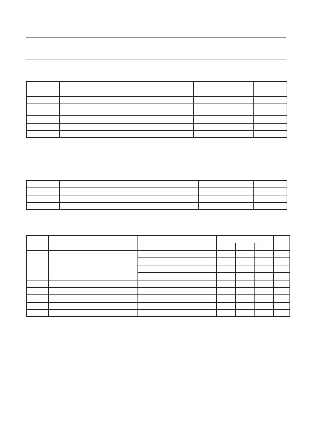
BLOCK DIAGRAM
SR01428
43215
20 19 18 17 16
761098
15 14 13 12 11
LO GND BYPASS
GND
V
CC
LNA
IN GND
MIXER
IN
MIXER
OUT
MIXER
OUT
PD1 PD2 GND
LNA
OUT
GND
OUT
GND
TANK
LNA
GND
GND GND
10pF 10pF
Figure 2. SA621 Block Diagram
Page 3
Philips Semiconductors Product specification
SA6211GHz low voltage LNA, mixer and VCO
1997 Nov 07
3
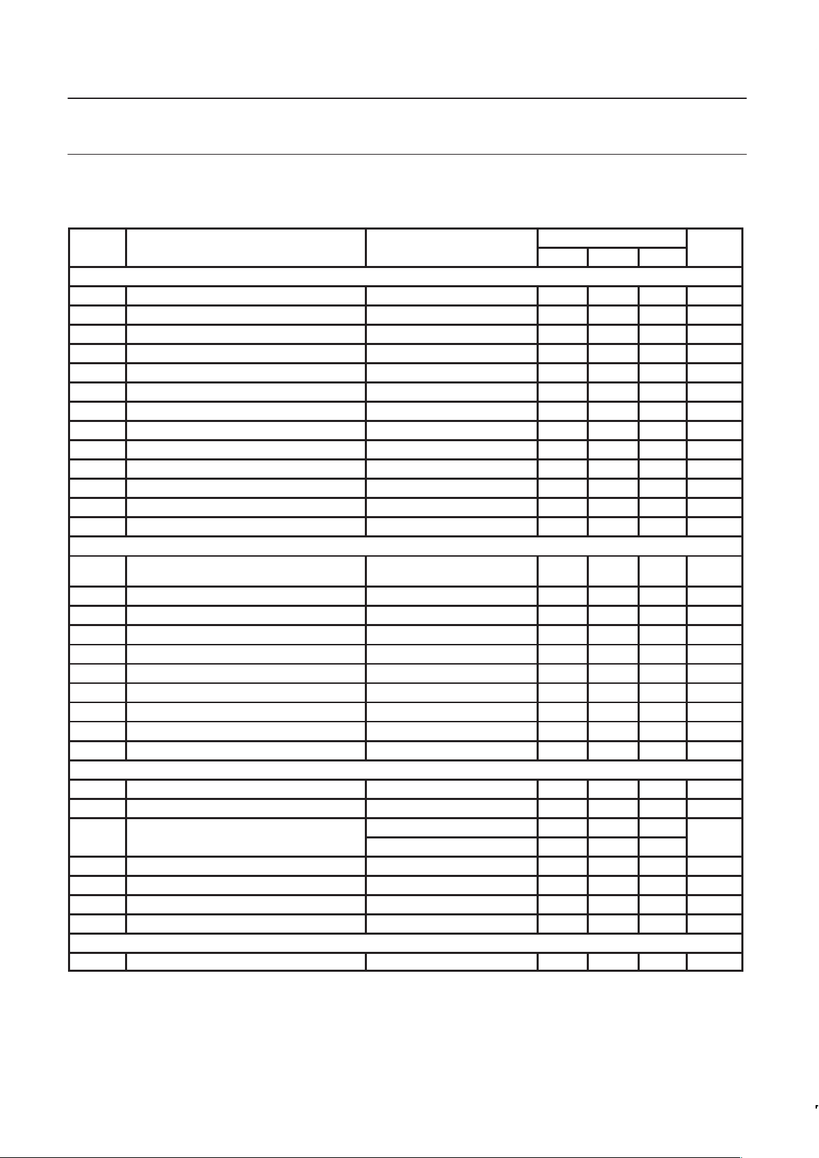
ABSOLUTE MAXIMUM RATINGS
SYMBOL PARAMETER RATING UNITS
V
CC
Supply voltage
1
-0.3 to +6 V
V
IN
Voltage applied to any other pin -0.3 to (VCC + 0.3) V
P
D
Power dissipation, TA = 25°C (still air)2
20-Pin Plastic SSOP
980 mW
T
JMAX
Maximum operating junction temperature 150 °C
P
MAX
Maximum power input/output +20 dBm
T
STG
Storage temperature range –65 to +150 °C
NOTE:
1. Transients exceeding 8V on V
CC
pin may damage product.
2. Maximum dissipation is determined by the operating ambient temperature and the thermal resistance,
θ
JA
: 20-Pin SSOP = 110°C/W
3. Pins 19 and 20 are ESD sensitive (mixer outputs).
RECOMMENDED OPERATING CONDITIONS
SYMBOL PARAMETER RA TING UNITS
V
CC
Supply voltage 2.7 to 5.5 V
T
A
Operating ambient temperature range -40 to +85 °C
T
J
Operating junction temperature -40 to +105 °C
DC ELECTRICAL CHARACTERISTICS
VCC = +3.0V , TA = 25°C; unless otherwise stated.
LIMITS
SYMBOL
PARAMETER
TEST CONDITIONS
MIN TYP MAX
UNITS
Full power-on 13.3 mA
pp
LNA powered-down 10 mA
ICCSu ly current
Standby (VCO + bias) 5.7 mA
Full power-down 20 µA
V
T
PD logic threshold voltage 1.2 1.6 1.8 V
V
IH
Logic 1 level 2.0 V
CC
V
V
IL
Logic 0 level –0.3 0.8 V
I
IL
PD1 input current Enable = 0.4V 10 µA
I
IH
PD2 input current Enable = 2.4V 10 µA
Page 4
Philips Semiconductors Product specification
SA6211GHz low voltage LNA, mixer and VCO
1997 Nov 07
4
AC ELECTRICAL CHARACTERISTICS
VCC = +3.0V , TA = 25°C; RFIN = 881MHz, f
VCO
= 964MHz; unless otherwise stated.
LIMITS
SYMBOL
PARAMETER
TEST CONDITIONS
–3
TYP
+3
UNITS
Low Noise Amplifier
f
RF
RF input frequency range 800 1000 MHz
S
21
Amplifier gain 15 dB
S
21
Amplifier gain in power-down mode -28 dB
∆S21/∆T Gain temperature sensitivity enabled 0.006 dB/°C
∆S21/∆f Gain frequency variation 800MHz - 1.0GHz ±0.013 dB/MHz
S
12
Amplifier reverse isolation @ 881 MHz -28 dB
S
11
Amplifier input match With ext. impedance matching -10 dB
S
22
Amplifier output match -10 dB
P
-1dB
Amplifier input 1dB gain compression -20 dBm
IP3 Amplifier input third order intercept -7 dBm
NF Amplifier noise figure 1.7 dB
t
ON
Amplifier turn-on time (Enable Lo → Hi) 120 µs
t
OFF
Amplifier turn-off time (Enable Hi → Lo) 0.3 µs
Mixer
PG
C
Mixer power conversion gain: RP = RL = 1.2kΩ,
fRF = 881MHz, fLO = 964MHz,
f
IF
= 83MHz
8.7 dB
S
11M
Mixer input match Ext. impedance matching req. -10 dB
NF
M
Mixer SSB noise figure 12 dB
P
-1dB
Mixer input 1dB gain compression -10 dBm
IP3
M
Mixer input third order intercept 4.5 dBm
IP
2INT
Mixer input second order intercept 15 dBm
P
RFM-IF
Mixer RF feedthrough RFIN = -25dBm -41 dBm
P
LO-IF
LO feedthrough to IF LO = -10dBm -23 dBm
P
LO-RFM
LO to mixer input feedthrough -52 dBm
P
LO-RF
LO to LNA input feedthrough -38 dBm
Voltage Controlled Oscillator (VCO)
1
f
VCO
VCO frequency range 883 1083 MHz
P
VCO
VCO power out See Figure 3 -10 -8 dBm
p
2
Offset = 30kHz -109
VCO hase noise
2
Offset = 60kHz -115
dBc/Hz
Harmonic content -22 dBc
Residual modulation 45 dB
Pulling figure VSWR=2:1, all phases ±500 kHz
Pushing figure ±100 kHz/V
Overall System
G
SYS
System gain LNA + Mixer 23.0 23.7 24.4 dB
NOTES:
1. VCO performance dependent on external components.
2. Based on copper-plated 2mm ceramic resonator (1/4 wave), f = 1025MHz, and can be improved by silver-plated or larger resonators.
Page 5
Philips Semiconductors Product specification
SA6211GHz low voltage LNA, mixer and VCO
1997 Nov 07
5
Table 1. Power ON/OFF Control Logic
PD1 PD2
0 0 Full chip power-down
0 1 or open VCO on, Mixer on, LNA power-down
1 or open 0 VCO on, LNA and Mixer power-down
1 or open 1 or open Full chip power-on (default)
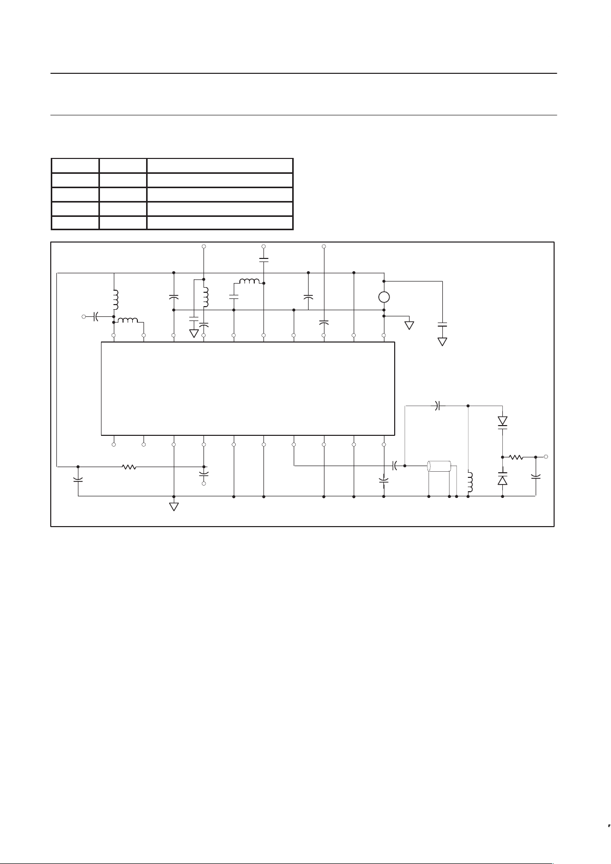
SR01424
+
–
20 19 18 17 16 15 14 13 12 11
12345678910
PD1 PD2 GND GND GND TANK GND GND BYPASS
MIXER GND GND GND GND
V
CC
LO
OUT
IF
OUT
VCO
OUT
SA621
C3
6.8pF
L1
560nH
L4
560nH
C2
10nF
C14
6.8pF
C13
33pF
C8
10nF
3V
C12
100pF
C1
100pF
V
CC
OUT
MIXER
OUT
MIXER
IN
LNA
IN
LNA
OUT
L3
6.8nH
10nF
0.1µF
C9
C11
L6
12nH
C10
2.2pF
C6
10nF
R2
24Ω
MURATA 2mm
1/4 WAVE
FREQ=1025MHz
C5
.5pF
C10
220pF
L7
18.5nH
Hi–Q
D1
R1
5.1kΩ
VCO
CONTROL
D7
10nF
C4
2.2pF
Figure 3. SA621 Applications Circuit
Page 6

Philips Semiconductors Product specification
SA6211GHz low voltage LNA, mixer and VCO
1997 Nov 07
6
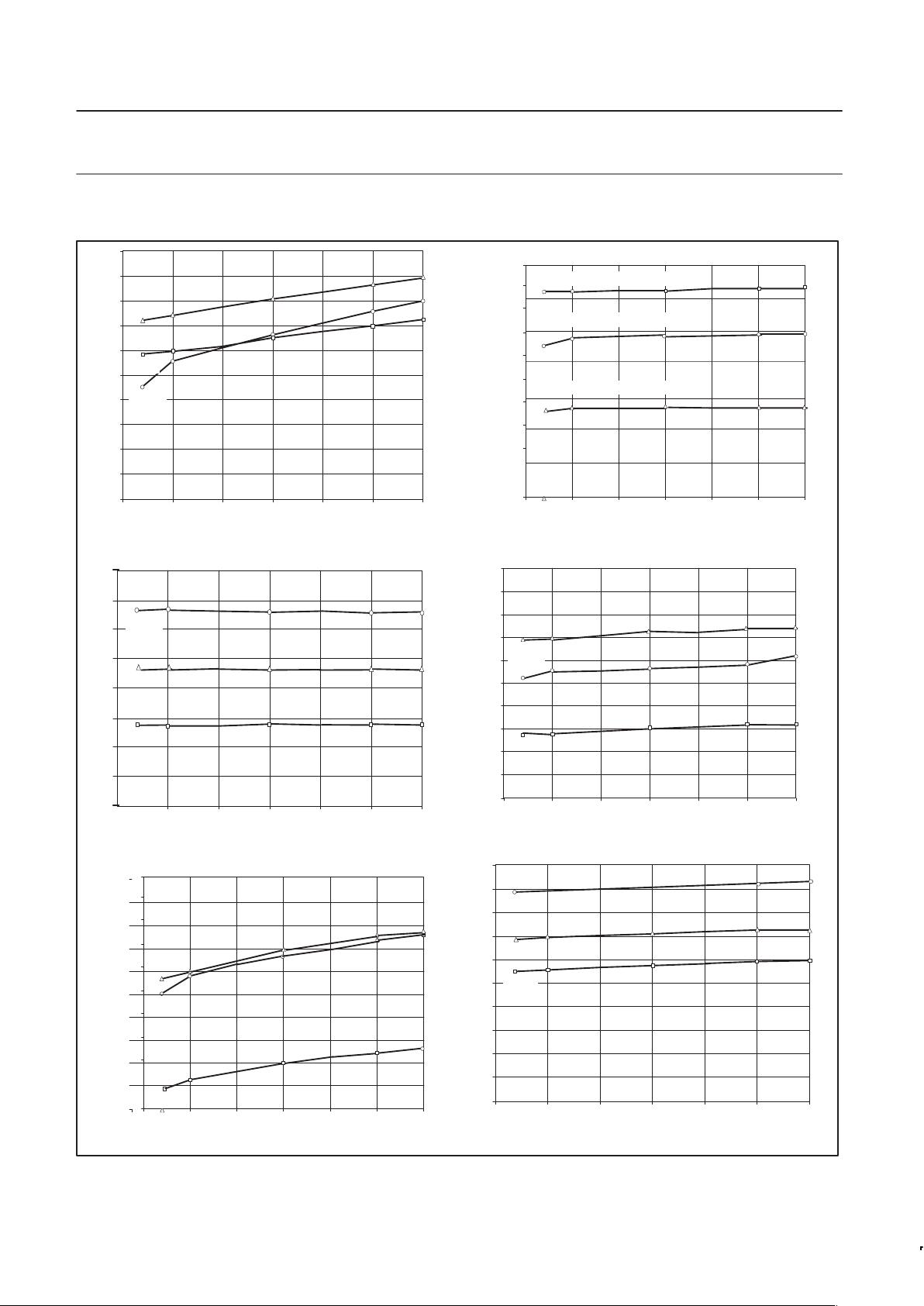
PERFORMANCE CHARACTERISTICS
SR01425
-15
2.5 3 3.5 4 4.5 5 5.5
V
CC
(V)
LNA 1dB (dBm)
-40°C
25°C
LNA 1dB Compression vs V
CC
-16
-17
-18
-19
-20
-21
-22
-23
-24
-25
-10.0
2.5 3 3.5 4 4.5 5 5.5
V
CC
(V)
MIXER 1dB (dBm)
-40°C
25°C
85°C
Mixer 1dB Compression vs V
CC
-10.5
-11.0
-11.5
-12.0
-9.0
-9.5
-28.0
2.5 3 3.5 4 4.5 5 5.5
VCC (V)
LNA GAIN (dB)
-40°C
25°C
85°C
LNA Gain (Disabled) vs V
CC
-28.5
-29.0
-29.5
-30.0
-30.5
-31.0
-27.0
-27.5
7.0
2.5 3 3.5 4 4.5 5 5.5
VCC (V)
MIXER IP3 (dBm)
-40°C
25°C
85°C
Mixer IP3 vs V
CC
6.5
6.0
5.5
5.0
4.5
4.0
3.5
3.0
-11
2.5 3 3.5 4 4.5 5 5.5
V
CC
(V)
LNA IP3 (dBm)
-40°C
25°C
LNA IP3 vs V
CC
-2
-3
-4
-5
-6
-7
-8
-9
-10
0
85°C
85°C
-12
VCC (V)
V POWER OUT (dBm)
VCO Power Out vs V
CC
CC
-6.00
2.5 3 3.5 4 4.5 5 5.5
-40°C
25°C
85°C
-7.00
-8.00
-9.00
-10.00
-11.00
-12.00
-4.00
-5.00
0
Figure 4.
Page 7
Philips Semiconductors Product specification
SA6211GHz low voltage LNA, mixer and VCO
1997 Nov 07
7
PERFORMANCE CHARACTERISTICS
SR01426
2.5 3 3.5 4 4.5 5 5.5
V
CC
(V)
I (mA)
-40°C
25°C
85°C
ICC vs VCC and Temperature
13.0
12.8
12.6
12.4
12.2
12.0
11.8
13.8
13.6
13.4
13.2
2.5 3 3.5 4 4.5 5 5.5
V
CC
(V)
MIXER GAIN (dB)
-40°C
85°C
Mixer Power Gain vs V
CC
2.5 3 3.5 4 4.5 5 5.5
V
CC
(V)
LO to LNA IN (dBm)
-40°C
25°C
85°C
LO to LNA In Feedthrough vs V
CC
2.5 3 3.5 4 4.5 5 5.5
V
CC
(V)
LO to MIXER IN (dBm)
-40°C
LO to Mixer In Feedthrough vs V
CC
-35
-36
-37
-38
-39
-40
-41
-42
-43
-44
-45
2.5 3 3.5 4 4.5 5 5.5
V
CC
(V)
LO to IF (dBm)
-40°C
25°C
85°C
LO to IF Feedthrough vs V
CC
-20
-21
-22
-23
-24
-25
-26
-27
-28
-29
-30
12
11
10
9
8
7
6
5
4
25°C
25°C
85°C
2.5 3 3.5 4 4.5 5 5.5
VCC (V)
ICC vs VCC at Room Temperature
14
12
10
8
6
4
0
ICC Full Chip Power–On
2
I
CC LNA Off, Mixer & VCO On
I
CC VCO On, LNA & Mixer Off
I (mA)
CC
-44
-46
-48
-50
-52
-54
-56
-58
-60
-62
-64
CC
Figure 5.
Page 8

Philips Semiconductors Product specification
SA6211GHz low voltage LNA, mixer and VCO
1997 Nov 07
8
PERFORMANCE CHARACTERISTICS
SR01427
2.5 3 3.5 4 4.5 5 5.5
V
CC
(V)
MIXER IN to IF (dBm)
-40°C
85°C
Mixer In to IF Feedthrough vs V
CC
15.0
2.5 3 3.5 4 4.5 5 5.5
V
CC
(V)
LNA GAIN (dB)
-40°C
25°C
85°C
LNA Gain (Enabled) vs V
CC
14.8
14.6
14.4
14.2
14.0
13.8
13.6
15.6
15.4
15.2
2.5 3 3.5 4 4.5 5 5.5
VCC (V)
MIXER NOISE FIGURE (dB)
-40°C
25°C
85°C
Mixer Noise Figure vs V
CC
12.5
12.4
12.3
12.2
12.1
12.0
11.9
11.8
11.7
11.6
11.5
2.5 3 3.5 4 4.5 5 5.5
V
CC
(V)
LNA NOISE FIGURE (dB)
-40°C
25°C
85°C
LNA Noise Figure vs V
CC
2.0
1.9
1.8
1.7
1.6
1.5
1.4
1.3
1.2
1.1
1.0
2.5 3 3.5 4 4.5 5 5.5
V
CC
(V)
85°C
VCO Phase Noise vs V
CC
@60kHz Offset
–100.0
–105.0
–110.0
–115.0
–120.0
–125.0
2.5 3 3.5 4 4.5 5 5.5
V
CC
(V)
VCO PHASE NOISE (dBc/Hz
VCO Phase Noise vs VCC @ 30kHz Offset
–100.0
–105.0
–110.0
–115.0
–120.0
–125.0
–95.0
25°C
40°C
85°C
–95.0
40°C
–35
–36
–37
–38
–39
–40
–41
–42
–43
–44
–45
25°C
VCO PHASE NOISE (dBc/Hz
Figure 6.
Page 9

Philips Semiconductors Product specification
SA6211GHz low voltage LNA, mixer and VCO
1997 Nov 07
9
CH2
S
11
1 U FS
3
2
1
4
1: 40.1 Ω
-129.6 Ω
200 MHz
2: 24.0 Ω
-62.9 Ω
400 MHz
3: 18.6 Ω
-37.4 Ω
600 MHz
START 100. 000 000 MHz STOP 1 200. 000 000 MHz
SR01252
4: 14.1 Ω
10.5 pF
-16.7 Ω
900 MHz
3
CH1
S
22
1 U FS
2
1
4
1: 40.5 Ω
-28.2 Ω
700 MHz
2: 36.1 Ω
-12.4 Ω
800 MHz
3: 34.7 Ω
3.5 Ω
900 MHz
START 700. 000 000 MHz STOP 1 200. 000 000 MHz
4: 34.9 Ω
3.74 Ω
661.4 pH
900 MHz
A. S11 DATA
B. S22 DATA
Figure 7. Typical S11 of LNA at 3V
Page 10

Philips Semiconductors Product specification
SA6211GHz low voltage LNA, mixer and VCO
1997 Nov 07
10
3
CH1
S
22
1 U FS
2
1
4
1: 40.5 Ω
-28.2 Ω
700 MHz
2: 36.1 Ω
-12.4 Ω
800 MHz
3: 34.7 Ω
3.5 Ω
900 MHz
START 700. 000 000 MHz STOP 1 200. 000 000 MHz
SR01253
4: 34.9 Ω
3.74 Ω
661.4 pH
900 MHz
Figure 8. Typical S22 of LNA at 3V
CH1
S
21
10 U FS
1: 6.7 U
142.5 °
200 MHz
2: 5.9 U
112.3 °
400 MHz
3: 5.9 U
78.1 °
600 MHz
START 100. 000 000 MHz STOP 1 200. 000 000 MHz
1
3
2
4
SR01254
4: 4.5 U
21.2°
900 MHz
Figure 9. Typical S21 of LNA at 3V
Page 11

Philips Semiconductors Product specification
SA6211GHz low voltage LNA, mixer and VCO
1997 Nov 07
11
CH2
S
12
50 mU FS
1: 1.9 mU
83.0 °
200 MHz
2: 1.6 mU
133.5 °
400 MHz
3: 11.4 mU
141.5 °
600 MHz
START 100. 000 000 MHz STOP 1 200. 000 000 MHz
3
2
4
SR01255
1
4: 27.9 mU
106.1°
900 MHz
Figure 10. Typical S12 of LNA at 3V
3
CH1
S
11
1 U FS
2
1
4
1: 122.8 Ω
-144.9 Ω
200 MHz
2: 58.0 Ω
-86.8 Ω
400 MHz
3: 45.9 Ω
-62.3 Ω
600 MHz
START 100. 000 000 MHz STOP 1 200. 000 000 MHz
SR01256
4: 26.6 Ω
-43.2 Ω
4.085 pF
900 MHz
Figure 11. Typical S11 of Mixer at 3V
Page 12

Philips Semiconductors Product specification
SA6211GHz low voltage LNA, mixer and VCO
1997 Nov 07
12
4
CH1
S
11
/M
1 U FS
2
1
3
1: -11.766 Ω
289.41 Ω
200 MHz
2: 11.953 Ω
134.05 Ω
400 MHz
3: 16.555 Ω
78.48 Ω
600 MHz
START 100. 000 000 MHz STOP 1 200. 000 000 MHz
SR01257
3: 18.652 Ω
31.516 Ω
5.5732 nH
900 MHz
Figure 12. Typical 1/S11 of VCO (Pin 7)at 3V
Page 13

Philips Semiconductors Product specification
SA6211GHz low voltage LNA, mixer and VCO
1997 Nov 07
13
Table 2. Typical S-Parameters of LNA at 3V
LNA
Freq (MHz)
|S11|
(U)
<S11 (deg)
|S21|
(U)
<S21 (deg)
|S12|
(U)
<S12 (deg)
|S22|
(U)
<S
22
(deg)
100 0.86 -20 7.4 160 0.001 92 0.59 -10
122 0.86 -24 7.1 156 0.001 62 0.58 -12
144 0.85 -28 7.0 151 0.001 105 0.58 -14
166 0.83 -32 6.9 148 0.000 92 0.57 -16
188 0.82 -36 6.8 144 0.002 100 0.57 -18
210 0.81 -41 6.7 140 0.002 74 0.56 -20
232 0.80 -45 6.6 136 0.002 100 0.55 -22
254 0.79 -48 6.5 133 0.001 84 0.54 -25
276 0.78 -52 6.4 130 0.001 103 0.53 -27
298 0.76 -56 6.3 126 0.002 94 0.52 -29
320 0.75 -59 6.3 123 0.002 67 0.51 -31
342 0.73 -63 6.2 119 0.002 108 0.50 -33
364 0.71 -66 6.1 116 0.002 118 0.48 -35
386 0.70 -69 6.0 113 0.001 103 0.47 -36
408 0.69 -72 5.9 111 0.001 176 0.46 -37
430 0.68 -76 5.9 109 0.004 174 0.45 -37
452 0.69 -78 6.0 106 0.006 162 0.46 -38
474 0.68 -82 6.1 102 0.007 160 0.47 -42
496 0.67 -85 6.1 97 0.008 153 0.47 -46
518 0.66 -89 6.1 93 0.010 146 0.46 -50
540 0.65 -92 6.1 89 0.009 142 0.45 -55
562 0.63 -96 6.1 85 0.010 138 0.43 -59
584 0.62 -99 6.0 81 0.011 146 0.42 -64
606 0.62 -102 5.9 77 0.011 141 0.40 -69
628 0.61 -104 5.8 72 0.013 137 0.38 -73
650 0.61 -107 5.7 69 0.013 131 0.36 -78
672 0.60 -109 5.7 65 0.016 130 0.34 -84
694 0.60 -112 5.6 61 0.016 132 0.31 -90
716 0.59 -115 5.5 57 0.017 129 0.29 -97
738 0.59 -118 5.5 53 0.019 128 0.27 -104
760 0.59 -121 5.3 48 0.021 123 0.24 -113
782 0.59 -124 5.3 44 0.021 122 0.22 -122
804 0.59 -126 5.1 40 0.022 120 0.21 -133
826 0.59 -129 5.0 36 0.024 118 0.19 -145
848 0.59 -132 4.9 31 0.026 116 0.18 -159
870 0.59 -135 4.8 26 0.027 112 0.17 -175
892 0.59 -138 4.6 22 0.028 108 0.18 169
914 0.59 -142 4.5 18 0.028 106 0.19 155
936 0.59 -144 4.3 14 0.028 106 0.20 142
958 0.59 -148 4.2 9 0.030 100 0.22 130
980 0.59 -151 4.0 4 0.031 99 0.24 120
1002 0.59 -153 3.8 0 0.031 95 0.26 111
1024 0.59 -157 3.6 -2 0.032 91 0.28 102
1046 0.59 -160 3.5 -6 0.032 86 0.30 95
1068 0.59 -164 3.3 -10 0.033 86 0.33 88
1090 0.59 -167 3.2 -14 0.033 81 0.35 82
1112 0.59 -170 3.0 -18 0.031 79 0.36 77
1134 0.58 -172 2.8 -22 0.030 46 0.38 72
1156 0.58 -175 2.7 -25 0.031 79 0.39 67
1178 0.57 -178 2.5 -28 0.031 74 0.41 63
1200 0.57 178 2.4 -31 0.029 72 0.42 59
Page 14

Philips Semiconductors Product specification
SA6211GHz low voltage LNA, mixer and VCO
1997 Nov 07
14
T able 3. Typical S-Parameters of Mixer at 3V
Mixer
Freq (MHz)
|S11|
(U)
<S11 (deg)
100 0.73 -11
122 0.73 -147
144 0.72 -16
166 0.72 -19
188 0.72 -21
210 0.71 -24
232 0.70 -27
254 0.70 -29
276 0.69 -32
298 0.68 -34
320 0.67 -37
342 0.66 -39
364 0.64 -42
386 0.63 -–44
408 0.62 -46
430 0.61 -48
452 0.59 -50
474 0.58 -52
496 0.57 -53
518 0.56 -54
540 0.55 -56
562 0.55 -57
584 0.54 -59
606 0.54 -61
628 0.54 -62
650 0.54 -64
Mixer
Freq (MHz)
|S11|
(U)
<S11 (deg)
672 0.54 -65
694 0.54 -67
716 0.54 -69
738 0.54 -71
760 0.54 -73
782 0.55 -76
804 0.55 -78
826 0.55 -80
848 0.55 -82
870 0.55 -85
892 0.56 -87
914 0.55 -90
936 0.56 -93
958 0.56 -96
980 0.56 -98
1002 0.56 -101
1024 0.57 -104
1046 0.57 -106
1068 0.57 -110
1090 0.57 -112
1112 0.57 -115
1134 0.57 -118
1156 0.57 -121
1178 0.57 -124
1200 0.57 -127
Page 15

Philips Semiconductors Product specification
SA6211GHz low voltage dLNA, mixer and VCO
1997 Nov 07
15
TSSOP20: plastic thin shrink small outline package; 20 leads; body width 4.4 mm SOT360-1
Page 16

Philips Semiconductors Product specification
SA6211GHz low voltage dLNA, mixer and VCO
1997 Nov 07
16
Philips Semiconductors and Philips Electronics North America Corporation reserve the right to make changes, without notice, in the products,
including circuits, standard cells, and/or software, described or contained herein in order to improve design and/or performance. Philips
Semiconductors assumes no responsibility or liability for the use of any of these products, conveys no license or title under any patent, copyright,
or mask work right to these products, and makes no representations or warranties that these products are free from patent, copyright, or mask
work right infringement, unless otherwise specified. Applications that are described herein for any of these products are for illustrative purposes
only. Philips Semiconductors makes no representation or warranty that such applications will be suitable for the specified use without further testing
or modification.
LIFE SUPPORT APPLICA TIONS
Philips Semiconductors and Philips Electronics North America Corporation Products are not designed for use in life support appliances, devices,
or systems where malfunction of a Philips Semiconductors and Philips Electronics North America Corporation Product can reasonably be expected
to result in a personal injury. Philips Semiconductors and Philips Electronics North America Corporation customers using or selling Philips
Semiconductors and Philips Electronics North America Corporation Products for use in such applications do so at their own risk and agree to fully
indemnify Philips Semiconductors and Philips Electronics North America Corporation for any damages resulting from such improper use or sale.
This data sheet contains preliminary data, and supplementary data will be published at a later date. Philips
Semiconductors reserves the right to make changes at any time without notice in order to improve design
and supply the best possible product.
Philips Semiconductors
811 East Arques Avenue
P.O. Box 3409
Sunnyvale, California 94088–3409
Telephone 800-234-7381
DEFINITIONS
Data Sheet Identification Product Status Definition
Objective Specification
Preliminary Specification
Product Specification
Formative or in Design
Preproduction Product
Full Production
This data sheet contains the design target or goal specifications for product development. Specifications
may change in any manner without notice.
This data sheet contains Final Specifications. Philips Semiconductors reserves the right to make changes
at any time without notice, in order to improve design and supply the best possible product.
Philips Semiconductors and Philips Electronics North America Corporation
register eligible circuits under the Semiconductor Chip Protection Act.
Copyright Philips Electronics North America Corporation 1996
All rights reserved. Printed in U.S.A.
 Loading...