

Page 1

S3C8248/C8245/P8245/C8247/C8249/P8249 PRODUCT OVERVIEW
1 PRODUCT OVERVIEW
S3C8-SERIES MICROCONTROLLERS
Samsung's S3C8 series of 8-bit single-chip CMOS microcontrollers offers a fast and efficient CPU, a wide range
of integrated peripherals, and various mask-programmable ROM sizes. Among the major CPU features are:
— Efficient register-oriented architecture
— Selectable CPU clock sources
— Idle and Stop power-down mode release by interrupt
— Built-in basic timer with watchdog function
A sophisticated interrupt structure recognizes up to eight interrupt levels. Each level can have one or more
interrupt sources and vectors. Fast interrupt processing (within a minimum of four CPU clocks) can be assigned
to specific interrupt levels.
S3C8248/C8245/P8245/C8247/C8249/P8249 MICROCONTROLLER
The S3C8248/C8245/P8245/C8247/C8249/P8249
single-chip CMOS microcontroller are fabricated
using the highly advanced CMOS process, based on
Samsung’s newest CPU architecture.
The S3C8248, S3C8245, S3C8247, S3C8249 are a
microcontroller with a 8K-byte, 16K-byte, 24K-byte.
32K-byte mask-programmable ROM embedded
respectively.
The S3P8245 is a microcontroller with a 16K-byte
one-time-programmable ROM embedded.
The S3P8249 is a microcontroller with a 32K-byte
one-time-programmable ROM embedded.
Using a proven modular design approach, Samsung
engineers have successfully developed the
S3C8248/C8245/P8245/C8247/C8249/P8249 by
integrating the following peripheral modules with the
powerful SAM8 core:
— Six programmable I/O ports, including five 8-bit
ports and one 5-bit port, for a total of 45 pins.
— Eight bit-programmable pins for external
interrupts.
— One 8-bit basic timer for oscillation stabilization
and watchdog functions (system reset).
— Two 8-bit timer/counter and two 16-bit
timer/counter with selectable operating modes.
— Watch timer for real time.
— 8-input A/D converter
— Serial I/O interface
The S3C8248/C8245/P8245/C8247/C8249/P8249
is versatile microcontroller for camera, LCD and
ADC application, etc. They are currently available in
80-pin TQFP and 80-pin QFP package
OTP
The S3P8245/P8249 are OTP (One Time Programmable) version of the S3C8245/C8249 microcontroller. The
S3P8245 microcontroller has an on-chip 16K-byte one-time-programmable EPROM instead of a masked ROM.
The S3P8249 microcontroller has an on-chip 32K-byte one-time-programmable EPROM instead of a masked
ROM. The S3P8245 is comparable to the S3P8245, both in function and in pin configuration.
The S3P8249 is comparable to the S3P8249, both in function and in pin configuration.
1-1
Page 2

PRODUCT OVERVIEW S3C8248/C8245/P8245/C8247/C8249/P8249
FEATURES
Memory
• ROM: 32K-byte (S3C8249/P8249)
• ROM: 16K-byte (S3C8245/P8245)
• RAM: 1056-Byte (S3C8249/P8249, S3C8247)
• RAM: 544-Byte (S3C8245/P8245, S3C8248)
• Data memory mapped I/O
Oscillation Sources
• Crystal, ceramic, RC (main)
• Crystal for subsystem clock
• Main system clock frequency 1-10 MHz
(3 MHz at 1.8 V, 10 MHz at 2.7 V)
• Subsystem clock frequency: 32.768 kHz
• CPU clock divider (1/1, 1/2, 1/8, 1/16)
Two Power-Down Modes
• Idle (only CPU clock stops)
• Stop (System clock stops)
Interrupts
• 6 level 8 vector 8 internal interrupt
• 2 level 8 vector 8 external interrupt
45 I/O Pins
• 45 configurable I/O pins
Basic Timer
• Overflow signal makes a system reset.
• Watchdog function
8-Bit Timer/Counter A
• Programmable 8-bit timer
• Interval, capture, PWM mode
• Match/capture, overflow interrupt
8-Bit Timer/Counter B
• Programmable 8-bit timer
• Carrier frequency generator
16-Bit Timer/Counter 0
• Programmable 16-bit timer
• Match interrupt generates
16-Bit Timer/Counter 1
• Programmable 16-bit timer
• Interval, capture, PWM mode
• Match/capture, overflow interrupt
Watch Timer
• Real-time and interval time measurement
• Clock generation for LCD
• Four frequency outputs for buzzer sound
LCD Controller/Driver
• Maximum 16-digit LCD direct drive capability
• Display modes: static, 1/2 duty (1/2 bias)
• 1/3 duty (1/2 or 1/3 bias), 1/4 duty (1/3 bias)
A/D Converter
• Eight analog input channels
• 50 µs conversion speed at 1 MHz f
ADC
clock
• 10-bit conversion resolution
8-Bit Serial I/O Interface
• 8-bit transmit/receive mode
• 8-bit receive mode
• LSB-first/MSB-first transmission selectable
• Internal/external clock source
Voltage Booster
• LCD display voltage supply
• S/W control en/disable
• 3.0 V drive
Voltage Detector
• Programmable detection voltage
(2.2 V, 2.4 V, 3.0 V, 4.0 V)
• En/Disable S/W selectable
Instruction Execution Times
• 400 ns at 10 MHz (main)
• 122 us at 32.768 kHz (subsystem)
Operating Temperature Range
• -40 °C to 85 °C
Operating Voltage Range
• 1.8 V to 5.5 V
Package Type
• 80-pin QFP
• 80-pin TQFP
S3C8249’s ROM version device
• S3C8247 (ROM 24K-byte)
S3C8245’s ROM version device
• S3C8248 (ROM 8K-byte)
1-2
Page 3
S3C8248/C8245/P8245/C8247/C8249/P8249 PRODUCT OVERVIEW
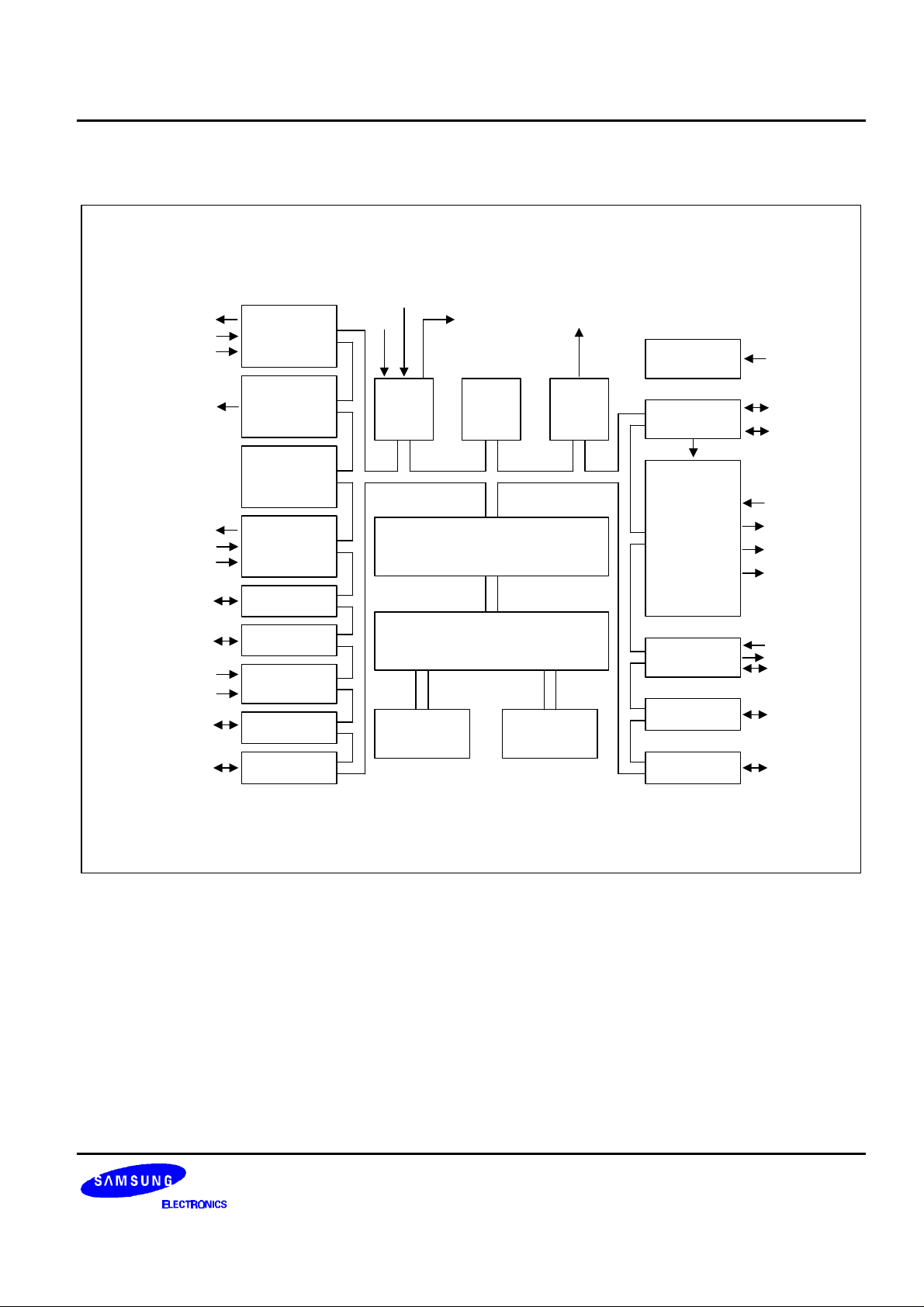
BLOCK DIAGRAM
X
XT
IN
TAOUT/TAPWM/P3.1
TACLK/P3.2
TACAP/P3.3
TBPWM/P3.0
T1CAP/P1.0
T1CLK/P1.1
T1OUT/T1PWM/P1.2
P0.0-P0.7/
INT0-INT7
8-Bit
Timer/
Counter A
8-Bit
Timer/
Counter B
16-Bit
Timer/
Counter 0
16-Bit
Timer/
Counter 1
I/O Port 0
RESET
IN
XOUT XTOUT
OSC/
RESET
I/O Port and Interrupt Control
Basic
Timer
BUZ/P1.4
Watch
Timer
Voltage
Detector
Voltage
Booster
LCD
Driver
VVLDREF
CB
CA
VLC0-VLC2
COM0-COM3
SEG0-SEG15
SEG16-SEG31
P1.0-P1.7
AVREF
AVSS
P2.0-P2.7/
ADC0-ADC7
P3.0-P3.4
I/O Port 1
A/D
Converter
I/O Port 2
I/O Port 3
SAM88 RC CPU
544/1056 Byte
Register File
16/32-Kbyte
ROM
Figure 1-1. Block Diagram
Serial I/O
Port
I/O Port 4
I/O Port 5
SI/P1.7
SO/P1.5
SCK/P1.6
P4.0-P4.7
P5.0-P5.7
1-3
Page 4

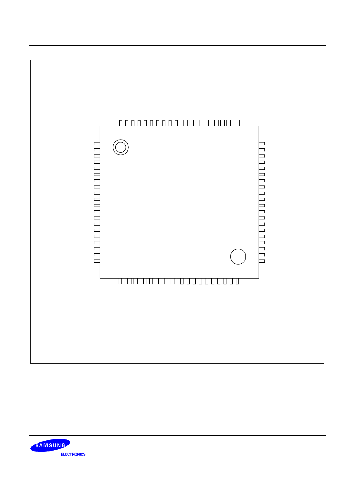
PRODUCT OVERVIEW S3C8248/C8245/P8245/C8247/C8249/P8249
PIN ASSIGNMENT
SEG25/P5.1
SEG24/P5.0
SEG23/P4.7
SEG22/P4.6
SEG21/P4.5
SEG20/P4.4
SEG19/P4.3
SEG18/P4.2
SEG17/P4.1
SEG16/P4.0
SEG15
SEG14
SEG13
SEG12
SEG11
SEG10
SEG26/P5.2
SEG27/P5.3
SEG28/P5.4
SEG29/P5.5
SEG30/P5.6
SEG31/P5.7
P3.0/TBPWM
P3.1/TAOUT/TAPWM
P3.2/TACLK
P3.3/TACAP/SDAT
P3.4/SCLK
VDD
VSS
XOUT
XIN
TEST
XTIN
XTOUT
RESET
P0.0/INT0
P0.1/INT1
P0.2/INT2
P0.3/INT3
P0.4/INT4
1
2
3
4
5
6
7
8
9
10
11
12
13
14
15
16
17
18
19
20
21
22
23
24
807978777675747372717069686766
S3C8248/C8245
/C8247/C8249
(80-QFP-1420C)
65
64
SEG9
63
SEG8
62
SEG7
61
SEG6
60
SEG5
59
SEG4
58
SEG3
57
SEG2
56
SEG1
55
SEG0
54
COM3
53
COM2
52
COM1
51
COM0
50
VLC2
49
VLC1
48
VLC0
47
CA
46
CB
45
AVSS
44
AVREF
43
P2.7/ADC7/VVLDREF
42
P2.6/ADC6
41
P2.5/ADC5
1-4
252627282830313233343536373839
P1.3
P1.7/SI
P1.5/SO
P1.4/BUZ
P0.5/INT5
P0.6/INT6
P0.7/INT7
P1.0/T1CAP
P1.1/T1CLK
P1.2/T1OUT/T1PWM
P1.6/SCK
P2.0/ADC0
P2.1/ADC1
40
P2.2/ADC3
P2.3/ADC4
P2.4/ADC4
Figure 1-2. S3C8248/C8245/C8247/C8249 Pin Assignments (80-QFP)
Page 5
S3C8248/C8245/P8245/C8247/C8249/P8249 PRODUCT OVERVIEW
SEG25/P5.1
SEG24/P5.0
SEG23/P4.7
SEG22/P4.6
SEG21/P4.5
SEG20/P4.4
SEG19/P4.3
SEG18/P4.2
SEG17/P4.1
SEG16/P4.0
SEG15
SEG14
SEG13
SEG12
SEG11
SEG10
SEG9
SEG8
SEG7
SEG6
SEG26/P5.2
SEG27/P5.3
SEG28/P5.4
SEG29/P5.5
SEG30/P5.6
SEG31/P5.7
P3.0/TBPWM
P3.1/TAOUT/TAPWM
P3.2/TACLK
P3.3/TACAP/SDAT
P3.4/SCLK
V
DD
V
X
OUT
X
TEST
XT
XT
OUT
RESET
P0.0/INT0
SS
80797877767574737271706968676665646362
1
2
3
4
5
6
7
8
9
10
11
12
13
S3C8248/C8245
/C8247/C8249
(80-TQFP-1212)
14
15
IN
16
17
IN
18
19
20
21222324252627282830313233343536373839
61
40
60
59
58
57
56
55
54
53
52
51
50
49
48
47
46
45
44
43
42
41
SEG5
SEG4
SEG3
SEG2
SEG1
SEG0
COM3
COM2
COM1
COM0
V
LC2
V
LC1
V
LC0
CA
CB
AV
SS
AV
REF
P2.7/ADC7/V
P2.6/ADC6
P2.5/ADC5
VLDREF
P1.3
P1.7/SI
P1.5/SO
P1.4/BUZ
P0.1/INT1
P0.2/INT2
P0.3/INT3
P0.4/INT4
P0.5/INT5
P0.6/INT6
P0.7/INT7
P1.0/T1CAP
P1.1/T1CLK
P1.6/SCK
P2.0/ADC0
P2.1/ADC1
P2.2/ADC3
P2.3/ADC4
P2.4/ADC4
P1.2/T1OUT/T1PWM
Figure 1-3. S3C8248/C8245/C8247/C8249 Pin Assignments (80-TQFP)
1-5
Page 6

PRODUCT OVERVIEW S3C8248/C8245/P8245/C8247/C8249/P8249
PIN DESCRIPTIONS
Table 1-1. S3C8248/C8245/C8247/C8249 Pin Descriptions
Pin
Names
P0.0–P0.7 I/O I/O port with bit programmable pins;
Pin
Type
Pin
Description
Circuit
Type
Pin
Numbers
(note)
Share
Pins
D–4 20–27 INT0–INT7
Schmitt trigger input or output mode
selected by software; software assignable
pull-up. P0.0–P0.7 can be used as inputs
for external interrupts INT0–INT7
(with noise filter and interrupt control).
P1.0–1.7 I/O I/O port with bit programmable pins; Input
or output mode selected by software;
Open-drain output mode can be selected
by software; software assignable pull-up.
Alternately P1.0–P1.7 can be used as SI,
E–2 28-35 SI, SO, SCK,
BUZ, T1CAP
T1CLK
T1OUT
T1PWM
SO, SCK, BUZ, T1CAP, T1CLK, T1OUT,
T1PWM
P2.0–P2.7 I/O I/O port with bit programmable pins;
normal input and AD input or output
mode selected by software; software
assignable pull-up.
P3.0–P3.4 I/O I/O port with bit programmable pins. Input
or push-pull output with software
assignable pull-up. Alternately P3.0–P3.3
can be used as TACAP, TACLK, TAOUT,
TAPWM, TBPWM
F–10
F–18
36–42,
43
ADC0–ADC6
V
VLDREF
(ADC7)
D–2 7–11 TACAP
TACLK
TAOUT
TAPWM
TBPWM
P4.0–P4.7 I/O I/O port with bit programmable pins.
H–14 71–78 SEG16–SEG23
Push-pull or open drain output and input
with software assignable pull-up.
P4.0–P4.7 can alternately be used as
outputs for LCD SEG
P5.0–P5.7 I/O Have the same characteristic as port 4 H–14 79–6 SEG24–SEG31
1-6
Page 7

S3C8248/C8245/P8245/C8247/C8249/P8249 PRODUCT OVERVIEW
Table 1-1. S3C8248/C8245/C8247/C8249 Pin Descriptions (Continued)
Pin
Names
ADC0–ADC6
ADC7
AV
REF
AV
SS
Pin
Type
I A/D converter analog input channels F–10
Pin
Description
Circuit
Type
F–18
Pin
Numbers
36–42
43
(note)
– A/D converter reference voltage – 44 –
– A/D converter ground – 45 –
Share
Pins
P2.0–P2.6
P2.7
INT0–INT7 I External interrupt input pins D–4 20–27 P0.0–P0.7
RESET
I System reset pin
B 19 –
(pull-up resistor: 250 kΩ)
TEST I 0 V: Normal MCU operating
– 16 –
5 V: Test mode
12 V: for OTP writing
SDAT, SCLK O Serial OTP interface pins; serial data
D–2 10, 11 P3.3, P3.4
and clock
V
DD, VSS
– Power input pins for CPU operation
– 12, 13 –
(internal) and Power input for OTP
Writing
X
OUT, XIN
– Main oscillator pins – 14, 15 –
SCK, SO, SI I/O Serial I/O interface clock signal E–2 33–35 P1.5–P1.7
V
VLDREF
I Voltage detector reference voltage
F–18 43 P2.7
input
TACAP I Timer A Capture input D–2 10 P3.3
TACLK I Timer A External clock input D–2 9 P3.2
TAOUT/TAPWM O Timer A output and PWM output D–2 8 P3.1
TBPWM O Timer B PWM output D–2 7 P3.0
T1CAP I Timer 1 Capture input E–2 28 P1.0
T1CLK I Timer 1 External clock input E–2 29 P1.1
T1OUT/T1PWM O Timer 1 output and PWM output E–2 30 P1.2
COM0–COM3 O LCD common signal output H 51–54 –
SEG0–SEG15 O LCD segment output H 55–70 –
SEG16–SEG23 O LCD segment output H–14 71–78 P4.0–P4.7
SEG24–SEG31 O LCD Segment output H–14 79–6 P5.0–P5.7
V
LC0–VLC2
BUZ O 0.5, 1, 2 or 4 kHz frequency output for
O LCD power supply – 48–50 –
E–2 32 P1.4
buzzer sound with 4.19 MHz main
system clock or 32768 Hz subsystem
clock
CA, CB – Capacitor terminal for voltage booster – 46–47 –
1-7
Page 8

PRODUCT OVERVIEW S3C8248/C8245/P8245/C8247/C8249/P8249
Disable
PIN CIRCUITS
VDD
VDD
Pull-up
Enable
P-Channel
In
Figure 1-4. Pin Circuit Type B (RESETRESET)
V
DD
Data
Output
P-Channel
N-Channel
Out
Data
Output
Disable
Circuit
Type C
Figure 1-6. Pin Circuit Type D-2 (P3)
VDD
VDD
Data
Output
Disable
Pin Circuit
Type C
I/O
Pull-up
Enable
I/O
1-8
Figure 1-5. Pin Circuit Type C
Noise
Ext.INT
Input
Normal
Filter
Figure 1-7. Pin Circuit Type D-4 (P0)
Page 9

S3C8248/C8245/P8245/C8247/C8249/P8249 PRODUCT OVERVIEW
VDD
VDD
Open drain
Enable
VDD
Pull-up
Resistor
Pull-up
Enable
Data
Output
Disable
Schmitt Trigger
Figure 1-8. Pin Circuit Type E-2 (P1)
Pull-up
Enable
P-CH
N-CH
VDD
I/O
Data
Output
Disable
ADC & VLD
Enable
Data
VLDREF
To ADC
Circuit
Type C
Figure 1-10. Pin Circuit Type F-18 (P2.7/VLD
VLC2
VLC1
I/O
REF
)
Data
Output
Disable
ADCEN
Data
To ADC
Circuit
Type C
Figure 1-9. Pin Circuit Type F-10 (P2.0–P2.6)
I/O
SEG/
COM
VLC0
Figure 1-11. Pin Circuit Type H (SEG/COM)
Out
1-9
Page 10

PRODUCT OVERVIEW S3C8248/C8245/P8245/C8247/C8249/P8249
VLC2
VLC1
SEG
Output
Disable
VLC0
Open Drain EN
Data
LCD Out EN
SEG
Output
Disable
Figure 1-12. Pin Circuit Type H-4
VDD
VDD
Pull-up
Enable
Circuit
Type H-4
1-10
Figure 1-13. Pin Circuit Type H-14 (P4, P5)
Page 11

S3C8248/C8245/P8245/C8247/C8249/P8249 ELECTRICAL DATA
19 ELECTRICAL DATA
OVERVIEW
In this chapter, S3C8248/C8245/C8247/C8249 electrical characteristics are presented in tables and graphs.
The information is arranged in the following order:
— Absolute maximum ratings
— Input/output capacitance
— D.C. electrical characteristics
— A.C. electrical characteristics
— Oscillation characteristics
— Oscillation stabilization time
— Data retention supply voltage in stop mode
— Serial I/O timing characteristics
— A/D converter electrical characteristics
19-1
Page 12

ELECTRICAL DATA S3C8248/C8245/P8245/C8247/C8249/P8249
Table 19-1. Absolute Maximum Ratings
(TA= 25 °C)
Parameter Symbol Conditions Rating Unit
Supply voltage
Input voltage
Output voltage
Output current high
V
DD
V
I
V
O
I
OH
One I/O pin active – 18 mA
– 0.3 to +6.5 V
– 0.3 to VDD + 0.3
– 0.3 to VDD + 0.3
All I/O pins active – 60
Output current low
I
OL
One I/O pin active + 30
Total pin current for port + 100
Operating temperature
Storage temperature
T
T
A
STG
– 40 to + 85
– 65 to + 150
°
C
Table 19-2. D.C. Electrical Characteristics
(T
= -40 °C to + 85 °C, VDD = 1.8 V to 5.5 V)
A
Parameter Symbol Conditions Min Typ Max Unit
Operating voltage
Input high voltage
Input low voltage
V
DD
V
IH1
V
IH2
V
IL1
V
IL2
f
= 10 MHz
CPU
f
= 3 MHz
CPU
All input pins except V
X
XT
,
IN
IN
All input pins except V
X
XT
,
IN
IN
IH2
IL2
2.7 – 5.5 V
1.8 – 5.5
0.8 V
DD
VDD-0.1
– –
–
–
V
DD
0.2 V
0.1
DD
19-2
Page 13

S3C8248/C8245/P8245/C8247/C8249/P8249 ELECTRICAL DATA
Table 19-2. D.C. Electrical Characteristics (Continued)
(T
= -40 °C to + 85 °C, VDD = 1.8 V to 5.5 V)
A
Parameter Symbol Conditions Min Typ Max Unit
Output high voltage
V
OH
V
= 5 V; IOH = -1 mA
DD
VDD–1.0
– – V
All output pins
Output low voltage
V
OL
V
= 5 V; IOL = 2 mA
DD
– – 0.4
All output pins
Input high leakage
current
Input low leakage
current
I
LIH1
I
LIH2
I
LIL1
I
LIL2
VIN = V
DD
All input pins except I
VIN = V
V
= 0 V
IN
DD, XIN
XT
,
IN
All input pins except I
V
= 0 V, X
IN
IN
XTIN,
,
– – 3 uA
LIH2
20
– – -3
LIL2
-20
RESET
Output high
leakage current
Output low leakage
current
Oscillator feed
back resistors
Pull-up resistor
I
I
R
LOH
LOL
osc1
R
V
= V
OUT
DD
All I/O pins and output pins
V
= 0 V
OUT
All I/O pins and output pins
V
= 5.0 V T
DD
X
L1
= V
IN
V
IN
, X
DD
= 0 V; V
OUT
DD
= 25 °C
A
= 0 V
= 5 V ±10 %
– – 3
– – -3
800 1000 1200
25 50 100
kΩ
Port 0,1,2,3,4,5 TA = 25°C
V
out voltage
LC0
(Booster run mode)
V
out voltage
LC1
(Booster run mode)
V
out voltage
LC2
(Booster run mode)
COM output
voltage deviation
SEG output
voltage deviation
R
L2
V
= 0 V; V
IN
= 5 V ±10%
DD
110 210 310
TA=25 °C, RESET only
V
LC0
TA = 25 °C, (1/3 bias mode)
TA = 25 °C, (1/2 bias mode)
V
LC1
TA = 25 °C (1/2 and 1/3
bias mode)
V
LC2
TA = 25 °C (1/3 bias mode)
0.9 1.0 1.1 V
1.4 1.5 1.7
2V
LC0
- 0.1
–
2V
LC0
+
0.1
3V
LC0
- 0.1
–
3V
LC0
+
0.1
V
DC
VDD = V
(V
-COMi)
LCD
LC2
= 3 V
–
± 60 ± 120
mV
IO = ± 15 µA (i = 0-3)
V
Ds
VDD = V
(V
-SEGi)
LCD
LC2
= 3 V
–
± 60 ± 120
IO = ± 15 µA (i = 0-31)
19-3
Page 14

ELECTRICAL DATA S3C8248/C8245/P8245/C8247/C8249/P8249
Table 19-2. D.C. Electrical Characteristics (Concluded)
(TA = -40 °C to + 85 °C, VDD = 1.8 V to 5.5 V)
Parameter Symbol Conditions Min Typ Max Unit
Supply current
(1)
I
DD1
(2)
V
= 5 V ± 10 %
DD
– 12 25 mA
10 MHz crystal oscillator
3 MHz crystal oscillator 4 10
V
= 3 V ± 10 %
DD
3 8
10 MHz crystal oscillator
3 MHz crystal oscillator 1 5
I
DD2
Idle mode: VDD = 5 V ± 10 %
– 3 10
10 MHz crystal oscillator
3 MHz crystal oscillator 1.5 4
Idle mode: VDD = 3 V± 10 %
1.2 3
10 MHz crystal oscillator
3 MHz crystal oscillator 0.5 1.5
I
DD3
Sub operating: main-osc stop
V
= 3 V ± 10 %
DD
– 20 40 uA
32768 Hz crystal oscillator
I
DD4
Sub idle mode: main-osc stop
V
= 3 V ± 10 %
DD
– 7 14
32768 Hz crystal oscillator
I
DD5
Main stop mode : sub-osc
stop V
V
DD
= 5 V ± 10 %
DD
= 3 V ± 10 %
– 1 3
0.5 2
NOTES:
1. Supply current does not include current drawn through internal pull-up resistors or external output current loads.
2. I
3. I
And does not include the LCD and Voltage booster and voltage level detector
4. I
5. Voltage booster’s operating voltage range is 2.0 V to 5.5 V. The range of 1.8 V to 2.0 V could be referenced
19-4
and I
DD1
and I
DD3
is the current when the main and subsystem clock oscillation stop.
DD5
in page 17-4.
include a power consumption of subsystem oscillator.
DD2
are the current when the main system clock oscillation stop and the subsystem clock is used.
DD4
Page 15

S3C8248/C8245/P8245/C8247/C8249/P8249 ELECTRICAL DATA
In case of S3C8248/C8245, the characteristic of VOH and VOL is differ with the characteristic of S3C8247/C8249
like as following. Other characteristics are same each other.
Table 19-3. D.C Electrical Characteristics of S3C8248/C8245
(T
= -40 °C to +85 °C, VDD = 1.8 V to 5.5 V)
A
Parameter Symbol Conditions Min Typ Max Unit
Output high voltage
V
V
OH1
OH2
VDD = 5 V; IOH = -1 mA
All output pins except V
VDD = 5 V; IOH = -6 mA
OH2
VDD-1.0
VDD-0.7
– – V
Port 3.0 only in S3C8248/C8245
Output low voltage
V
V
OL1
OL2
VDD = 5 V; IOL = 2 mA
All output pins except V
VDD = 5 V; IOH = 12 mA
– – 0.4
OL2
0.7
Port 3.0 only in S3C8248/C8245
19-5
Page 16

ELECTRICAL DATA S3C8248/C8245/P8245/C8247/C8249/P8249
Table 19-4. A.C. Electrical Characteristics
(T
= -40 °C to +85 °C, VDD = 1.8 V to 5.5 V)
A
Parameter Symbol Conditions Min Typ Max Unit
Interrupt input
high, low width
tINTH,
tINTL
P0.0–P0.7, VDD = 5 V
200 – ns
(P0.0–P0.7)
RESET input low
tRSL
VDD = 5 V
1 – – us
width
NOTE: User must keep more large value then min value.
tTIHtTIL
0.8 VDD
Figure 19-1. Input Timing for External Interrupts (Ports 0)
t
RSL
RESET
Figure 19-2. Input Timing for RESET
0.2 V
0.2 VDD0.2 VDD
DD
19-6
Page 17

S3C8248/C8245/P8245/C8247/C8249/P8249 ELECTRICAL DATA
Table 19-5. Input/Output Capacitance
(T
= -40 °C to +85 °C, V
A
DD
= 0 V )
Parameter Symbol Conditions Min Typ Max Unit
C
C
OUT
IN
f = 1 MHz; unmeasured pins
are returned to V
SS
– – 10 pF
Input
capacitance
Output
capacitance
I/O capacitance
C
IO
Table 19-6. Data Retention Supply Voltage in Stop Mode
(TA = -40 °C to + 85 °C)
Parameter Symbol Conditions Min Typ Max Unit
Data retention
V
DDDR
2
–
5.5 V
supply voltage
Data retention
I
DDDR
V
DDDR
= 2 V
– – 3 uA
supply current
V
DD
RESET
NOTE: t
~
~
~
~
Execution of
STOP Instrction
WAIT
is the same as 4096 x 16 x 1/fxx
Stop Mode
Data Retention Mode
V
DDDR
0.2 V
RESET
Occurs
DD
Oscillation
Stabilization
t
WAIT
Figure 19-3. Stop Mode Release Timing Initiated by RESET
Time
Normal
Operating Mode
19-7
Page 18

ELECTRICAL DATA S3C8248/C8245/P8245/C8247/C8249/P8249
Oscillation
Stabilization Time
~
~
Stop Mode
Idle Mode
V
Interrupt
NOTE: t
Data Retention Mode
V
DDDR
0.2 V
DD
DD
~
~
Execution of
STOP Instruction
WAIT
is the same as 4096 x 16 x BT clock
Figure 19-4. Stop Mode (Main) Release Timing Initiated by Interrupts
Oscillation
Stabilization Time
~
~
Stop Mode
t
WAIT
Normal
Operating Mode
Idle Mode
19-8
VDD
Interrupt
~
~
Execution of
STOP Instruction
NOTE: When the case of select the fxx/128 for basic timer input
clock before enter the stop mode.
tWAIT = 128 x 16 x (1/32768) = 62.5 ms
Data Retention Mode
VDDDR
0.2 VDD
tWAIT
Figure 19-5. Stop Mode (Sub) Release Timing Initiated by Interrupts
Normal
Operating Mode
Page 19

S3C8248/C8245/P8245/C8247/C8249/P8249 ELECTRICAL DATA
Table 19-7. A/D Converter Electrical Characteristics
(TA = - 40 °C to +85 °C, VDD = 1.8 V to 5.5 V, VSS = 0 V)
Parameter Symbol Conditions Min Typ Max Unit
Resolution – 10 – bit
Total accuracy
VDD = 5 V
AV
= 5 V
REF
– –
±3
LSB
AVSS = 0 V
Integral Linearity
ILE –
Error
Differential Linearity
DLE –
Error
Offset Error of Top EOT
Offset Error of
EOB
Bottom
Conversion time
(1)
Analog input voltage
Analog input
t
CON
V
R
IAN
AN
impedance
Analog reference
AV
REF
voltage
Analog ground
Analog input current
Analog block
current
(2)
AV
I
ADIN
I
ADC
SS
– – 40 – fxx
–
– 2 1000 – Mohm
– 2.5 –
–
AV
= VDD = 5 V
REF
AV
= VDD = 5 V
REF
AV
= VDD = 3 V
REF
AV
= VDD = 5 V
REF
When power down mode
±2
±1
±1 ±3
±0.5 ±2
AV
V
SS
SS
–
–
AV
REF
V
DD
VSS + 0.3
– – 10 uA
– 1 3 mA
0.5 1.5
100 500 nA
V
V
NOTES:
1. 'Conversion time' is the time required from the moment a conversion operation starts until it ends.
2. I
is an operating current during A/D conversion.
ADC
19-9
Page 20

ELECTRICAL DATA S3C8248/C8245/P8245/C8247/C8249/P8249
Table 19-8. Synchronous SIO Electrical Characteristics
(T
= -40 °C to +85 °C, VDD = 1.8 V to 5.5 V, VSS = 0 V, fxx = 10 MHz oscillator)
A
Parameter Symbol Conditions Min Typ Max Unit
SCK Cycle time
Serial Clock High Width
Serial Clock Low Width
Serial Output data delay
t
CYC
t
SCKH
t
SCKL
t
OD
– 200 – – ns
– 60 – –
– 60 – –
– – – 50
time
Serial Input data setup
t
ID
– 40 – –
time
Serial Input data Hold
t
IH
– 100 – –
time
SCK
SO
SI
t
OD
t
SCKL
t
ID
t
CYC
Input Data
Output Data
t
SCKH
0.8 V
DD
0.2 V
DD
t
IH
0.8 V
DD
0.2 V
DD
19-10
Figure 19-6. Serial Data Transfer Timing
Page 21

S3C8248/C8245/P8245/C8247/C8249/P8249 ELECTRICAL DATA
(TA = -40 °C to +85 °C, V
Table 19-9. Main Oscillator Frequency (f
= 1.8 V to 5.5 V)
DD
OSC1
)
Oscillator Clock Circuit Test Condition Min Typ Max Unit
Crystal
Ceramic
X
IN
C1 C2
X
IN
X
X
OUT
OUT
Crystal oscillation frequency 1 – 10 MHz
Ceramic oscillation
1 – 10 MHz
frequency
C1 C2
External clock
X
IN
X
OUT
XIN input frequency
1 – 10 MHz
RC
XIN XOUT
R
Table 19-10. Main Oscillator Clock Stabilization Time (t
(T
= -40 °C to +85 °C, VDD = 4.5 V to 5.5 V)
A
r = 35 kΩ, V
DD
= 5 V
2 MHz
)
ST1
Oscillator Test Condition Min Typ Max Unit
Crystal
Ceramic
VDD = 4.5 V to 5.5 V
Stabilization occurs when VDD is equal to the minimum
– – 10 ms
– – 4 ms
oscillator voltage range.
External clock
NOTE: Oscillation stabilization time (t
frequency after a power-on occurs, or when Stop mode is ended by a RESET signal.
The RESET should therefore be held at low level until the t
XIN input high and low level width (tXH, tXL)
) is the time required for the CPU clock to return to its normal oscillation
ST1
time has elapsed
ST1
50 – – ns
19-11
Page 22

ELECTRICAL DATA S3C8248/C8245/P8245/C8247/C8249/P8249
1 / f
OSC1
t
XH
OSC2
V
DD
IN
– 0. 5
0.4 V
V
)
X
IN
(TA = -40 °C + 85 °C, V
Figure 19-7. Clock Timing Measurement at X
Table 19-11. Sub Oscillator Frequency (f
= 1.8 V to 5.5 V)
DD
t
XL
Oscillator Clock Circuit Test Condition Min Typ Max Unit
Crystal
XTIN XTOUT
R
Crystal oscillation frequency
C1 = 22 pF, C2 = 33 pF
32 32.768 35 kHz
R = 39 KΩ
C1 C2
XTIN and XT
are connected
OUT
with R and C by soldering.
(T
A
= 25 °C)
Table 19-12. Sub Oscillator(crystal) Stabilization Time (t
ST2
)
Oscillator Test Condition Min Typ Max Unit
normal mode
strong mode
NOTE: Oscillation stabilization time (t
released by interrupts. The value Typ and Max are measured by buzzer output signal after stop release.
For example in voltage range of 4.5 V to 5.5 V of normal mode, we can see the buzzer output signal within 400 ms
at our test condition.
19-12
VDD = 4.5 V to 5.5 V
VDD = 1.8 V to 3.0 V
VDD = 4.5 V to 5.5 V
VDD = 1.8 V to 3.0 V
) is the time required for the oscillator to it’s normal oscillation when stop mode is
ST2
– 250 500 ms
– – 2 s
– – 2 s
– 250 500 ms
Page 23

S3C8248/C8245/P8245/C8247/C8249/P8249 ELECTRICAL DATA
fCPU
10 MHz
8 MHZ
3 MHZ
1 MHz
B
A
1 2 3 4 5 6 7
2.71.8
Supply Voltage (V)
Minimum instruction clock = 1/4 x oscillator frequency
5.5
Figure 19-8. Operating Voltage Range
19-13
Page 24

S3C8248/C8245/P8245/C8247/C8249/P8249 MECHANICAL DATA
20 MECHANICAL DATA
OVERVIEW
The S3C8248/C8245/C8247/C8249 microcontroller is currently available in 80-pin-QFP/TQFP package.
23.90
± 0.30
17.90 ± 0.30
14.00 ± 0.20
#80
0.80
#1
20.00
± 0.20
80-QFP-1420C
0.35
+ 0.10
0.15 MAX
(0.80)
0-8
+ 0.10
0.15
- 0.05
0.10 MAX
0.80 ± 0.20
0.05 MIN
2.65
± 0.10
3.00 MAX
0.80
± 0.20
NOTE
: Dimensions are in millimeters.
Figure 20-1. Package Dimensions (80-QFP-1420C)
20-1
Page 25

MECHANICAL DATA S3C8248/C8245/P8245/C8247/C8249/P8249
14.00 BSC
12.00 BSC
14.00 BSC
#80
0.50
#1
12.00 BSC
80-TQFP-1212
0.17-0.27
0.08 MAX
0-7
0.09-0.20
0.60 ± 0.15
M
(1.25)
0.05-0.15
1.00
±
0.05
NOTE
: Dimensions are in millimeters.
Figure 20-2. Package Dimensions (80-TQFP-1212)
1.20 MAX
20-2
Page 26

S3C8248/C8245/P8245/C8247/C8249/P8249 S3P8245/P8249 OTP
21 S3P8245/P8249 OTP
OVERVIEW
The S3P8245/P8249 single-chip CMOS microcontroller is the OTP (One Time Programmable) version of the
S3C8248/C8245/C8247/C8249 microcontroller. It has an on-chip OTP ROM instead of a masked ROM. The
EPROM is accessed by serial data format.
The S3P8245/P8249 is fully compatible with the S3C8248/C8245/C8247/C8249, both in function and in pin
configuration. Because of its simple programming requirements, the S3P8245/P8249 is ideal as an evaluation
chip for the S3C8248/C8245/C8247/C8249.
21-1
Page 27

S3P8245/P8249 OTP S3C8248/C8245/P8245/C8247/C8249/P8249
SEG25/P5.1
SEG24/P5.0
SEG23/P4.7
SEG22/P4.6
SEG21/P4.5
SEG20/P4.4
SEG19/P4.3
SEG18/P4.2
SEG17/P4.1
SEG16/P4.0
SEG15
SEG14
SEG13
SEG12
SEG11
SEG10
SEF26/P5.2
SEG27/P5.3
SEG28/P5.4
SEG29/P5.5
SEG30/P5.6
SEG31/P5.7
P3.0/TBPWM
P3.1/TAOUT/TAPWM
P3.2/TACLK
P3.3/TACAP/SDAT
P3.4/SCLK
VDD
VSS
XOUT
XIN
VPP/TEST
XTIN
XTOUT
RESET
P0.0/INT0
P0.1/INT1
P0.2/INT2
P0.3/INT3
P0.4/INT4
807978777675747372717069686766
1
2
3
4
5
6
7
8
9
10
11
12
13
14
15
16
17
18
19
20
21
22
23
24
S3P8245/P8249
80-QFP
(Top View)
252627282930313233343536373839
65
SEG9
64
SEG8
63
SEG7
62
SEG6
61
SEG5
60
SEG4
59
SEG3
58
SEG2
57
SEG1
56
SEG0
55
COM3
54
COM2
53
COM1
52
COM0
51
VLC2
50
VLC1
49
VLC0
48
CA
47
CB
46
AVSS
45
AVREF
44
P2.7/ADC7/VVLDREF
43
P2.6/ADC6
42
P2.5/ADC5
41
40
21-2
P1.3
P1.7/SI
P1.5/SIO
P1.4/BUZ
P0.5/INT5
P0.6/INT6
P0.7/INT7
P1.1/T1CLK
P1.0/T1CAP
P1.2//T1OUT/T1PWM
P1.6/SCK
P2.0/ADC0
P2.1/ADC1
P2.2/ADC2
P2.3/ADC3
Figure 21-1. Pin Assignments (80-QFP)
P2.4/ADC4
Page 28

S3C8248/C8245/P8245/C8247/C8249/P8249 S3P8245/P8249 OTP
Table 21-1. Descriptions of Pins Used to Read/Write the EPROM
Main Chip During Programming
Pin Name Pin Name Pin No. I/O Function
P2.0 SDAT
10 I/O
Serial data pin. Output port when reading and
input port when writing. Can be assigned as a
Input/push-pull output port.
P2.1 SCLK
V
PP
TEST
11 I
16 I
Serial clock pin. Input only pin.
Power supply pin for EPROM cell writing
(indicates that OTP enters into the writing mode).
When 12.5 V is applied, OTP is in writing mode
and when 5 V is applied, OTP is in reading
mode. (Option)
RESET RESET
VDD/V
SS
VDD/V
SS
19 I
Chip Initialization
12/13 – Logic power supply pin. V
should be tied to
DD
+5 V during programming.
Table 21-2. Comparison of S3P8245/P8249 and S3C8248/C8245/C8247/C8249 Features
Characteristic S3P8245/P8249 S3C8248/C8245/C8247/C8249
Program Memory 16K/32K-byte EPROM 16K/32K-byte mask ROM
Operating Voltage (VDD) 1.8 V to 5.5 V 1.8 V to 5.5 V
OTP Programming Mode VDD = 5 V, V
(TEST) = 12.5 V
PP
Pin Configuration 80-QFP/80-TQFP 80-QFP/80-TQFP
EPROM Programmability User Program 1 time Programmed at the factory
21-3
Page 29

S3P8245/P8249 OTP S3C8248/C8245/P8245/C8247/C8249/P8249
OPERATING MODE CHARACTERISTICS
When 12.5 V is supplied to the VPP (TEST) pin of the S3P8245/P8249, the EPROM programming mode is
entered. The operating mode (read, write, or read protection) is selected according to the input signals to the pins
listed in Table 21-3 below.
Table 21-3. Operating Mode Selection Criteria
V
DD
5 V 5 V 0 0000H 1
NOTE: "0" means Low level; "1" means High level.
V
(TEST)
PP
REG/MEMMEM
Address(A15–A0) R/W Mode
12.5 V 0 0000H 0
12.5 V 0 0000H 1
12.5 V 1 0E3FH 0
EPROM read
EPROM program
EPROM verify
EPROM read protection
Table 21-4. D.C Electrical Characteristics
(T
= -40 °C to +85 °C, VDD = 1.8 V to 5.5 V)
A
Parameter Symbol Conditions Min Typ Max Unit
Operating voltage
Input high
voltage
Input low voltage
V
DD
V
IH1
V
IH2
V
IH3
V
V
f
= 10 MHz 2.7 – 5.5 V
CPU
All input pins except V
Port 4,5 V
XIN, XT
All input pins except V
XIN, XT
IL1
V
= 5 V; IOH = -1 mA
IL2
DD
IH2, 3
≥ V
LCD2
IN
IN
DD
IL2
1.8 – 5.5
0.8 V
0.8 V
DD
DD
– V
– V
VDD- 0.1 – V
– – 0.2 V
DD
DD
DD
0.1
All output pins
Output high voltage
V
OH
V
= 5 V; IOL = 2 mA
DD
VDD -1.0 – –
All output pins
Output low voltage
V
OL
– – 0.4
DD
21-4
Page 30

S3C8248/C8245/P8245/C8247/C8249/P8249 S3P8245/P8249 OTP
Table 21-4. D.C. Electrical Characteristics (Continued)
(T
= -40 °C to +85 °C, VDD = 1.8 V to 5.5 V)
A
Parameter Symbol Conditions Min Typ Max Unit
Input high leakage
current
Input low leakage
current
Output high
leakage current
Output low leakage
current
Oscillator feed
back resistors
Pull-up resistor
I
I
I
I
I
I
R
LIH1
LIH2
LIL1
LIL2
LOH
LOL
osc1
R
VIN = V
DD
All input pins except I
VIN = V
X
V
,
IN
= 0 V
IN
XT
DD
IN
All input pins except I
V
= 0 V
IN
X
XT
RESET
,
= V
,
IN
DD
V
IN
OUT
All I/O pins and Output pins
V
= 0 V
OUT
All I/O pins and Output pins
V
= 5.0 V T
DD
X
= V
, X
DD
= 0 V; V
OUT
DD
L1
IN
V
IN
LIH2
LIL2
= 25 °C
A
= 0 V
= 5 V ±10 %
– – 3
20
– – -3
-20 uA
– – 3
– – -3
800 1000 1200
25 50 100
kΩ
Port 0,1,2,3,4,5 TA = 25°C
V
out voltage
LC0
(Booster run mode)
V
out voltage
LC1
(Booster run mode)
V
out voltage
LC2
(Booster run mode)
COM output
voltage deviation
SEG output
voltage deviation
R
L2
V
IN
= 0 V; V
= 5 V ±10%
DD
110 210 310
TA=25 °C, RESET only
V
LC0
TA = 25 °C (1/3 bias mode)
TA = 25 °C (1/2 bias mode)
V
LC1
TA = 25 °C
0.9 1.0 1.1 V
1.4 1.5 1.7
2V
- 0.1 – 2V
LC0
LC0
+
0.1
V
LC2
TA = 25 °C
3V
- 0.1 – 3V
LC0
LC0
+
0.1
V
DC
VDD = V
LC2
= 3 V
–
± 60 ± 120
mV
(VLC-COMi)
IO = ± 15 µA (1 = 0–3)
V
Ds
VDD = V
LC2
= 3 V
–
± 60 ± 120
(VLC-COMi)
IO = ± 15 µA (1 = 0–3)
21-5
Page 31

S3P8245/P8249 OTP S3C8248/C8245/P8245/C8247/C8249/P8249
Table 21-4. D.C. Electrical Characteristics (Concluded)
(TA = -40 °C to + 85 °C, VDD = 1.8 V to 5.5 V)
Parameter Symbol Conditions Min Typ Max Unit
Supply current
(1)
I
DD1
(2)
V
= 5 V ± 10 %
DD
– 12 25 mA
10 MHz crystal oscillator
3 MHz crystal oscillator
V
= 3 V ± 10 %
DD
4 10
3 8
10 MHz crystal oscillator
1 5
3 10
I
DD2
3 MHz crystal oscillator
Idle mode: VDD = 5 V ± 10 %
10 MHz crystal oscillator
3 MHz crystal oscillator
Idle mode: VDD = 3 V± 10 %
1.5 4
1.2 3
10 MHz crystal oscillator
0.5 1.5
I
DD3
3 MHz crystal oscillator
Sub operating: main-osc stop
V
= 3 V ± 10 %
DD
– 20 40 uA
32768 Hz crystal oscillator
I
DD4
Sub idle mode: main-osc stop
V
= 3 V ± 10 %
DD
– 7 14
32768 Hz crystal oscillator
I
DD5
Main stop mode : sub-osc
stop V
V
DD
= 5 V ± 10 %
DD
= 3 V ± 10 % 0.5 2
– 1 3
NOTES:
1. Supply current does not include current drawn through internal pull-up resistors or external output current loads.
2. IDD and I
3. I
4. I
21-6
and I
DD3
is the current when the main and subsystem clock oscillation stop.
DD5
include a power consumption of subsystem oscillator.
DD2
are the current when the main system clock oscillation stop and the subsystem clock is used.
DD4
Page 32

S3C8248/C8245/P8245/C8247/C8249/P8249 S3P8245/P8249 OTP
case of S3P8245, the characteristic of VOH and VOL is differ with the characteristic of S3P8249 like as bellow.
Other characteristics are same each other.
Table 21-5. D.C Electrical Characteristics of S3C8248/C8245
(T
= -40 °C to +85 °C, VDD = 1.8 V to 5.5 V)
A
Parameter Symbol Conditions Min Typ Max Unit
Output high voltage
V
V
OH1
OH2
VDD = 5 V; IOH = -1 mA
All output pins except V
VDD = 5 V; IOH = -6 mA
VDD-1.0 – – V
OH2
VDD-0.7
Port 3.0 only in S3P8245
Output low voltage
V
V
OL1
OL2
VDD = 5 V; IOL = 2 Ma
All output pins except V
VDD = 5 V; IOH = 12 mA
– – 0.4
OL2
0.7
Port 3.0 only in S3P8245
21-7
Page 33

S3P8245/P8249 OTP S3C8248/C8245/P8245/C8247/C8249/P8249
fCPU
10 MHz
8 MHZ
3 MHZ
1 MHz
B
A
1 2 3 4 5 6 7
2.71.8
Supply Voltage (V)
Minimum instruction clock = 1/4 x oscillator frequency
5.5
Figure 21-2. Operating Voltage Range
21-8
 Loading...