

Page 1

Product Overview
Address Spaces
Addressing Modes
Control Registers
Interrupt Structure
Instruction Set
Page 2

S3C8444 PRODUCT OVERVIEW
1PRODUCT OVERVIEW
SAM8 PRODUCT FAMILY
Samsung's new SAM8 family of 8-bit single-chip CMOS microcontrollers offers a fast and efficient CPU, a wide
range of integrated peripherals, and various mask-programmable ROM sizes.
A dual address/data bus architecture and a large number of bit- or nibble-configurable I/O ports provide a flexible
programming environment for applications with varied memory and I/O requirements.
Timer/counters with selectable operating modes are included to support real-time operations. Many SAM8
microcontrollers have an external interface that provides access to external memory and other peripheral
devices.
The sophisticated interrupt structure recognizes up to eight interrupt levels. Each level can have one or more
interrupt sources and vectors. Fast interrupt processing (within a minimum six CPU clocks) can be assigned to
specific interrupt levels.
S3C8444 MICROCONTROLLER
The S3C8444 single-chip microcontroller is fabricated using a highly advanced CMOS process. Its design is
based on the powerful SAM8 CPU core. Stop and Idle power-down modes were implemented to reduce power
consumption. The size of the internal register file is logically expanded, increasing the addressable on-chip
register space to 1040 bytes. A flexible yet sophisticated external interface is used to access up to 64-Kbytes of
program and data memory. The S3C8444 is a versatile microcontroller that is ideal for use in a wide range of
general-purpose applications such as CD-ROM/DVD-ROM drives.
Using the SAM8 modular design approach, the following peripherals were integrated with the SAM8 CPU core:
1–1
Page 3

PRODUCT OVERVIEW S3C8444
— Six configurable 8-bit general I/O ports
— One 8-bit n-channel, open-drain output port
— One 8-bit input port for A/D converter input or
digital input
— Full-duplex serial data port with one
synchronous and three asynchronous (UART)
operating modes
— Two 8-bit timers with interval timer or PWM
mode
— Two 16-bit timer/counters with four
programmable operating modes
— Two programmable 8-bit PWM modules with
corresponding output pins
— One 8-bit capture module with CAP input pin
— A/D converter with 8 selectable input pins
The S3C8444 is a versatile microcontroller that is
ideal for use in a wide range of general-purpose
ROM-less applications such as CD-ROM/DVD-ROM
drivers.
Figure 1–1. S3C8444 Microcontroller
1–2
Page 4

S3C8444 PRODUCT OVERVIEW
FEATURES
CPU
• SAM8 CPU core
Memory
• 1040-byte of internal register file
• 4-kbyte internal program memory area
External Interface
• 64-Kbyte external data memory area
• 64-Kbyte external program memory (ROMless)
• 60-Kbyte external program memory (normal)
Instruction Set
• 78 instructions
• IDLE and STOP instructions
Instruction Execution Time
• 240 ns at 25 MHz f
Interrupts
• 20 interrupt sources and 19 interrupt vectors
• Seven interrupt levels
• Fast interrupt processing (level0 and 3-7 only)
(minimum)
OSC
General I/O
• Six 8-bit general I/O ports (ports 0,1,2,3,4, and
5)
• One 8-bit n-channel, open-drain output port
(port 6)
• One 8-bit input port (for ADC input or port 7
digital input)
Serial Port
• Full-duplex serial data port (UART)
• Four programmable operating modes
PWM and Capture
• Two output channels (PWM0, PWM1)
• 8-bit resolution with 2-bit prescaler
• 97.66-kHz frequency (25-MHz CPU clock)
• Capture module with CAP input pin
Analog-to-Digital Converter
• Eight analog input pins
• 8-bit conversion resolution
• 7.68-µs conversion speed (25-MHz CPU clock)
Operating Temperature Range
• – 20°C to + 85°C
Timer/Counters
• Two 8-bit timers with interval timer or PWM
mode (timers A and B)
• Two 16-bit timer/counters with four
programmable operating modes (timers C and
D)
Operating Voltage Range
• 4.5 V to 5.5 V
Package Type
• 80-pin QFP, 80–pin TQFP
1–3
Page 5
PRODUCT OVERVIEW S3C8444
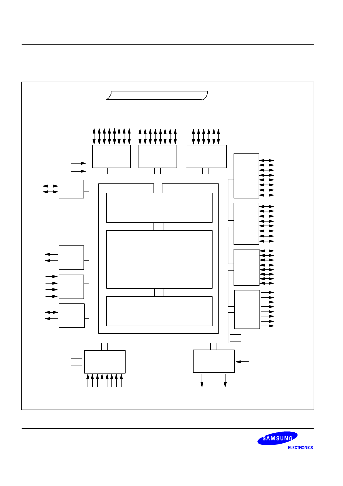
BLOCK DIAGRAM
EXTERNAL ADDRESS/DATA BUS
P2.6
P2.7
TA
TB
TCCK
TDCK
TCG
TDG
RESET
EA
PORT2
TIMERS
A and B
TIMERS
C and D
P0.0–P0.7
(A8–A15)
PORT 0
P1.0–P1.7
(AD0–AD7)
PORT 1 PORT 2
SAM8 BUS
PORT I/O & INTERRUPT
CONTROL
SAM8 CPU
P2.0–P2.5
(Control Signal)
PORT 3
PORT 4
PORT 5
P3.0–P3.7
P4.0–P4.7
P5.0–P5.3
P5.4–P5.7
1–4
RxD
TxD
AV
AV
SERIAL
PORT
SS
REF
A/D
CONVERTER
ADC0 /P7.0 –
ADC7 /P7.7
Figure 1–2. S3C8444 Block Diagram
1040-BYTE
REGISTER FILE
SAM8 BUS
PWM
MODULE
PWM0 PWM1
PORT 6 P6.0–P6.7
V
DD1
,V
SS1
V
DD2
,V
SS2
CAPTURE (P3.6)
Page 6
S3C8444 PRODUCT OVERVIEW
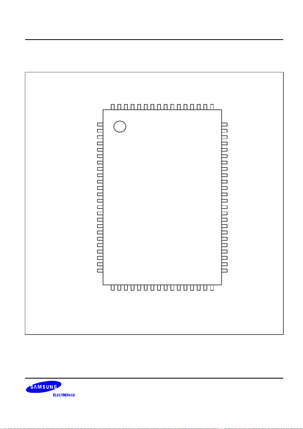
PIN ASSIGNMENTS
P1.7 / AD7
P1.6 / AD6
P1.5 / AD5
P1.4 / AD4
P1.3 / AD3
P1.2 / AD2
P1.1 / AD1
P1.0 / AD0
V
P0.7 / A15
P0.6 / A14
P0.5 / A13
P0.4 / A12
P0.3 / A11
P0.2 / A10
78
79
80
77
76
75
DD1
(int.)
74
73
72
71
70
69
68
67
66
EA
65
P0.1 / A9
P0.0 / A8
VDD2 (ext. )
P2.7 / TB
P2.6 / TA
P2.5 / PM
P2.4 / MR
P2.3 / DM
P2.2 /
P2.1 / DS
P2.0 / AS
PWM1
PWM0
P3.0 / TCCK / INT0
P5.7
P5.6
P5.5
P5.4
P5.3
P5.2
P5.1
P5.0
MW
RxD
TxD
1
2
3
4
5
6
7
8
9
10
11
12
13
14
15
16
17
18
19
20
21
22
23
24
27
26
25
28
29
S3C8444
80-QFP
(TOP VIEW)
33
32
31
30
34
35
36
37
38
39
40
64
63
62
61
60
59
58
57
56
55
54
53
52
51
50
49
48
47
46
45
44
43
42
41
RESET
NC
AS
VSS1 (int.)
XOUT
XIN
P6.0
P6.1
P6.2
P6.3
P6.4
P6.5
P6.6
P6.7
P7.7 / ADC7
P7.6 / ADC6
P7.5 / ADC5
P7.4 / ADC4
P7.3 / ADC3
AVSS
P7.2 / ADC2
P7.1 / ADC1
AVREF
P7.0 / ADC0
P3.1 / TDCK / INT1
SS2
(ext.)
P4.4 / INT8
P4.3 / INT7
P4.2 / INT6
P4.1 / INT5
P4.0 / INT4
V
P3.7 / WAIT
P3.6 / CAP
P3.5
P3.4
P3.3 / TDG / INT3
P3.2 / TCG / INT2
Figure 1–3. S3C8444 Pin Assignments
P4.7 / INT11
P4.6 / INT10
P4.5 / INT9
1–5
Page 7
PRODUCT OVERVIEW S3C8444
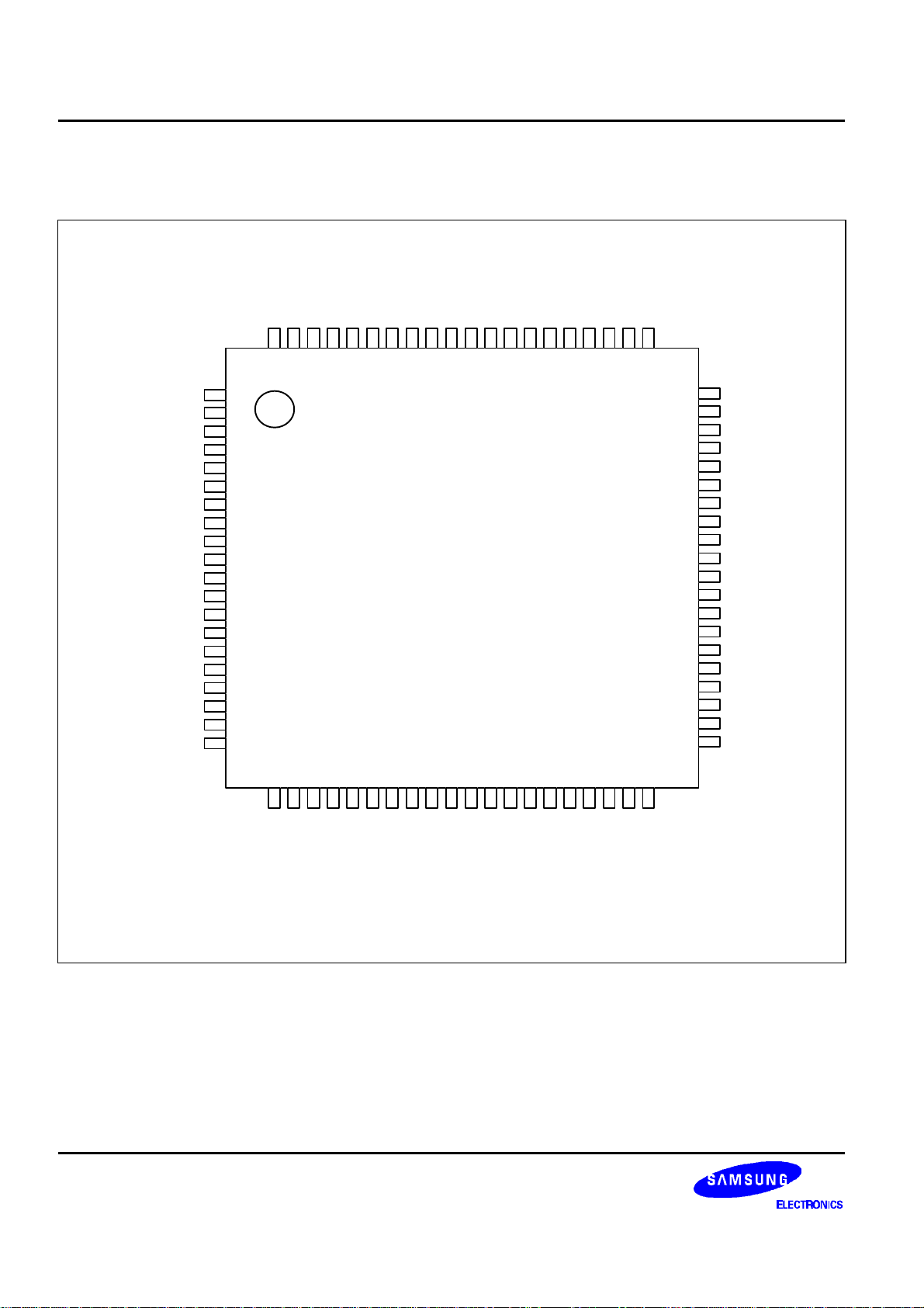
PIN ASSIGNMENTS (Continued)
P1.7 / AD7
P1.6 / AD6
P1.5 / AD5
P1.4 / AD4
P1.3 / AD3
P1.2 / AD2
P1.1 / AD1
P1.0 / AD0
V
P0.7 / A15
P0.6 / A14
P0.5 / A13
P0.4 / A12
P0.3 / A11
P0.2 / A10
P0.1 / A9
78
79
80
77
76
75
74
DD1
(int.)
73
72
71
70
69
68
67
66
65
EA
64
RESET
NC
62
63
AS
61
P0.0 / A8
P5.7
P5.6
P5.5
P5.4
P5.3
P5.2
P5.1
P5.0
V
(ext.
DD2
P2.7 / TB
P2.6 / TA
P2.5 / PM
P2.4 / MR
P2.3 / DM
P2.2 /
MW
P2.1 / DS
P2.0 / AS
RxD
TxD
1
2
3
4
5
6
7
8
9
)
10
11
12
13
14
15
16
17
18
19
20
25
24
23
22
21
P3.2 / TCG / INT2
P3.1 / TDCK / INT1
P3.0 / TCCK / INT0
PWM0
PWM1
S3C8444
80-TQFP
(TOP VIEW)
31
30
29
28
27
26
V
P3.7 /
P3.6 / CAP
P3.5
P3.4
P3.3 / TDG / INT3
SS2
(ext.)
WAIT
35
34
33
32
P4.3 / INT7
P4.2 / INT6
P4.1 / INT5
P4.0 / INT4
39
38
37
36
P4.7 / INT11
P4.6 / INT10
P4.5 / INT9
P4.4 / INT8
60
59
58
57
56
55
54
53
52
51
50
49
48
47
46
45
44
43
42
41
40
P7.0 / ADC0
Vss1 (int.)
X
OUT
X
IN
P6.0
P6.1
P6.2
P6.3
P6.4
P6.5
P6.6
P6.7
P7.7 / ADC7
P7.6 / ADC6
P7.5 / ADC5
P7.4 / ADC4
P7.3 / ADC3
AV
SS
P7.2 / ADC2
P7.1 / ADC1
AV
REF
1–6
Figure 1–4. S3C8444 Pin Assignments
Page 8
S3C8444 PRODUCT OVERVIEW
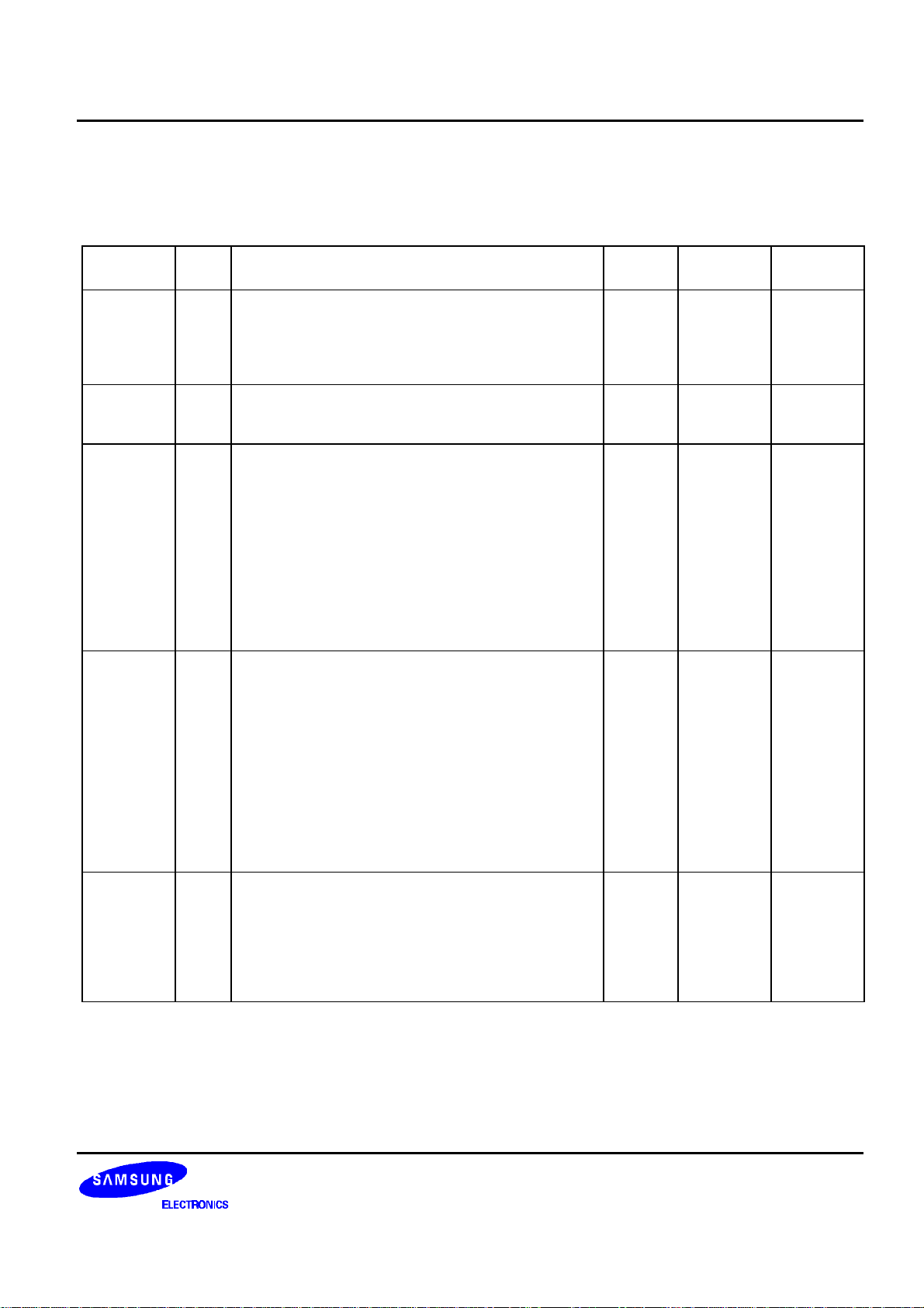
PIN DESCRIPTIONS
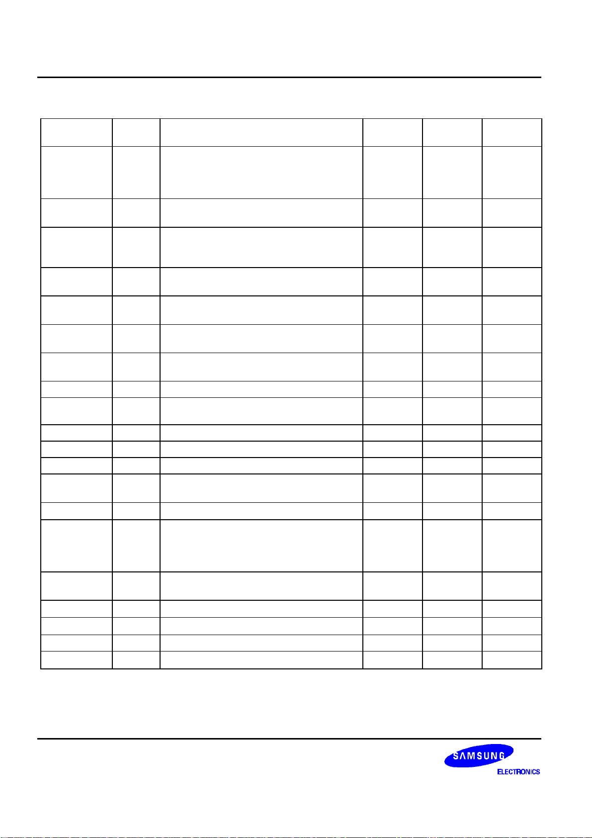
Table 1–1. S3C8444 Pin Descriptions
Pin
Name
P0.0 - P0.7 I/O Nibble programmable port; input or output mode
P1.0 - P1.7 I/O Same general characteristics as port 0; alternately
P2.0 - P2.7 I/O General I/O port with Schmitt trigger input or push-
P3.0 - P3.7 I/O General I/O port with bit programmable pins.
P4.0 - P4.7 I/O General I/O port with bit programmable pins.
Pin
Type
Pin
Description
selected by software; Schmitt trigger input or pushpull, open-drain output with software assignable
pull-ups; alternately configurable as external
interface address lines A8 - A15.
configurable as external interface address/data
lines AD0 - AD7.
pull output. bit programmable;
P2.0 / Address Strobe (AS)
P2.1 / Data Strobe (DS)
P2.2 / Memory Write (MW)
P2.3 / Data Memory select (DM)
P2.4 / Memory Read (MR)
P2.5 / Program Memory select (PM)
P2.6 / timer A output (TA)
P2.7 / timer B output (TB)
Schmitt trigger input or push-pull output with
software assignable pull-ups. Input or output mode
is selectable by software. P3.0 - P3.3 are alternately
used as inputs for external interrupts INT0-INT3,
respectively (with noise filters and interrupt control):
P3.0 / timer C clock input (TCCK) / INT0
P3.1 / timer D clock input (TDCK) / INT1
P3.2 / timer C gate input (TCG) / INT2
P3.3 / timer D gate input (TDG) / INT3
P3.6 / Capture data input (CAP)
P3.7 / WAIT for slow memory interface
Schmitt trigger input or push-pull, open-drain output
with software assignable pull-ups. Input or output
mode is selectable by software. P4.0-P4.7 can
alternately be used as inputs for external interrupts
INT4-INT11, respectively (with noise filters and
interrupt control)
Circuit
Type
3 2, 1,
3 73-66 AD0 - AD7
5 19 - 12
4 24-31 (See pin
4 33-40 INT4 -
QFP Pin
Number
80-75
Share
A8 - A15
AS, DS,
MW, DM,
MR, PM,
TA, TB
description)
INT11
Pins
1–7
Page 9
PRODUCT OVERVIEW S3C8444
Table 1–1. S3C8444 Pin Descriptions (Continued)
Pin
Name
P5.0–P5.7
P6.0–P6.7
ADC0–ADC7
AV
, AV
REF
SS
RxD
TxD
PWM0,
PWM1
TA, TB
INT0–INT11
TCCK, TDCK
TCG, TDG
CAP
WAIT
RESET
EA
V
, V
DD1
SS1
V
, V
DD2
SS2
XIN, X
OUT
AS
NC
Pin
Type
I/O
General I/O port with nibble programmable
Pin
Description
Circuit
Type
QFP Pin
Number
3 10–3 —
pins. Schmitt trigger input or push-pull,
open-drain output mode. Mode and pull-ups
are assigned by software.
O
N-channel, open-drain output port; the pin
8 58–51 —
circuits can withstand loads up to 9 volts.
I
Analog input pins for A/D converter module.
Alternatively used as general-purpose
2 41, 43–44,
46–50
P7.0–P7.7
digital input port 7.
—
A/D converter reference voltage and
— 42, 45 —
ground
I/O
Serial data RxD pin for receive input and
6 20 —
transmit output (mode 0)
O
Serial data TxD pin for transmit output and
7 21 —
shift clock input (mode 0)
O
O
Pulse width modulation output pins
Output pins for timer A and timer B
I
External interrupt input pins
I
External clock input for timer C and timer D
I
Gate input pins for timer C and timer D
I
Capture data input for PWM module
I
Input pin for the slow memory timing signal
7 23, 22 —
5 13, 12 P2.6, P2.7
4 24–27,
33–40
P3.0–P3.3,
P4.0–P4.7
4 24, 25 P3.0, P3.1
4 26, 27 P3.2, P3.3
4 30 P3.6
4 31 P3.7
from the external interface
I
System reset pin (pull-up resistor: 220 kΩ)
I
External access (EA) pin with two modes:
1 64 —
— 65 —
5 V input: normal ROM-less operation with
external interface (0 V is not allowed)
9 V–10 V input: for factory test mode
—
Power input pins for CPU operation
— 74, 61 —
(internal)
—
—
O
Power input pins for port output (external)
Main oscillator pins
Address strobe
— 11, 32 —
— 59, 60 —
7 62 —
— No connection pins (connect to VSS) — 62, 63 —
Share
Pins
NOTE VDD1 must be connected to VDD2 in users application circuit, VSS1 & VSS2 also.
1–8
Page 10
S3C8444 PRODUCT OVERVIEW
PIN CIRCUITS
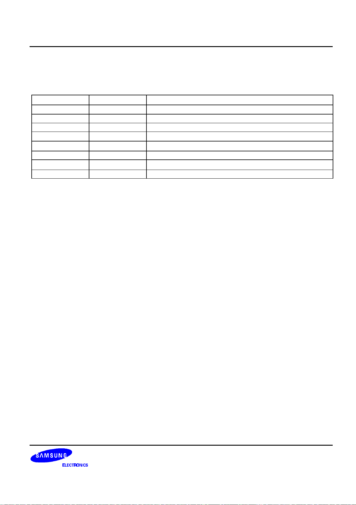
Table 1–2. Pin Circuit Assignments for the S3C8444
Circuit Number Circuit Type S3C8444 Assignments
1 Input
2 Input
3 I/O
4 I/O
5 I/O
6 I/O
7 Output
8 Output
RESET pin
A/D converter input pins, ADC0–ADC7
Port 0, 1, and 5
Ports 3 and 4, TCCK, TDCK, TCG, TDG, CAP, WAIT, INT0–INT11
Port 2 (AS, DS, MW, DM, MR, PM, TA,TB)
Serial port RxD pin
Serial port TxD pin, PWM0, PWM1 and AS
Port 6 (n-channel, open-drain output with high current capability)
1–9
Page 11
PRODUCT OVERVIEW S3C8444
V
DD
PULL-UP
RESISTOR
(Typical 230 kΩ)
INPUT
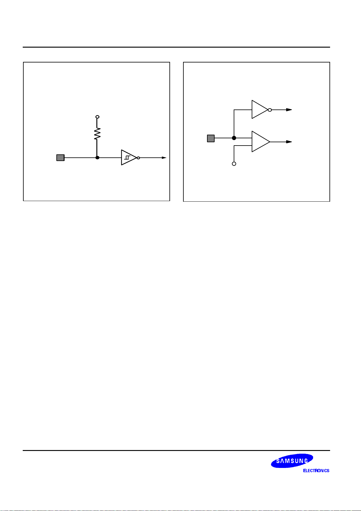
Figure 1–5. Pin Circuit Type 1 (RESETRESET)
INPUT
BUFFER
IN
V
+
–
REF
ADC
LOGIC
Figure 1–6. Pin Circuit Type 2 (ADC0–ADC7)
1–10
Page 12
S3C8444 PRODUCT OVERVIEW
V
DD
PULL-UP
RESISTOR
(Ty pical 46 kΩ)
PULL-UP
ENABLE
V
DD
DAT A
IN / OUT
OPENDRAIN
OUTPUT
DISABLE
V
SS
INPUT
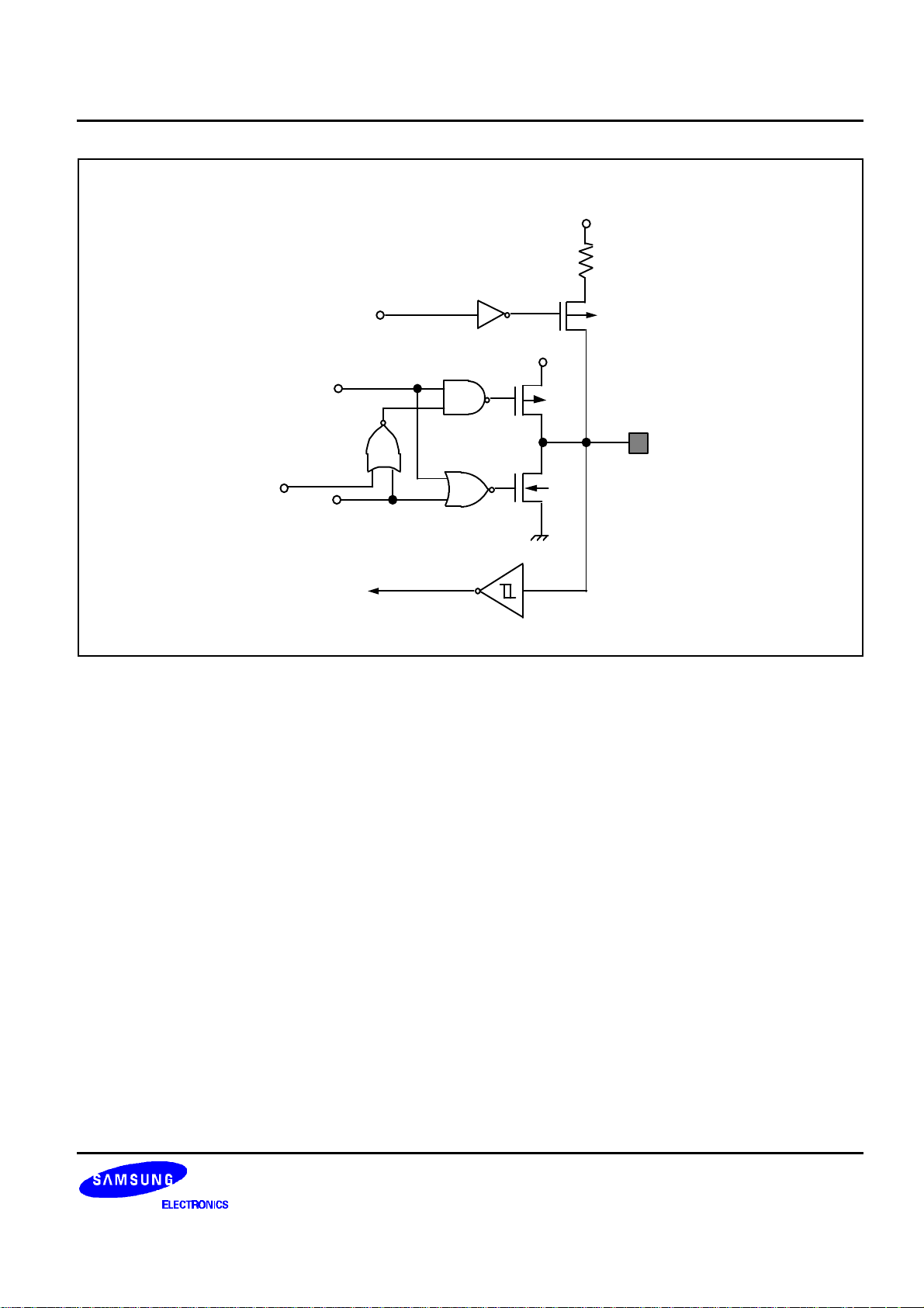
Figure 1–7. Pin Circuit Type 3 (Ports 0,1, and 5)
1–11
Page 13
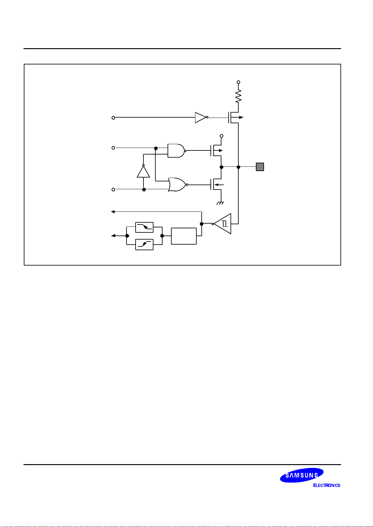
PRODUCT OVERVIEW S3C8444
V
DD
PULL-UP
RESISTOR
(Typical 46 kΩ)
PULL-UP
ENABLE
DATA
OUTPUT
DISABLE
INPUT
V
DD
IN / OUT
V
SS
EXTERNAL
INTERRUPT
INPUT
NOISE
FILTER
Figure 1–8. Pin Circuit Type 4
(Ports 3 and 4, TCCK, TDCK, TCG, TDG, CAP, WAIT, WAIT, INT0–INT11)
1–12
Page 14
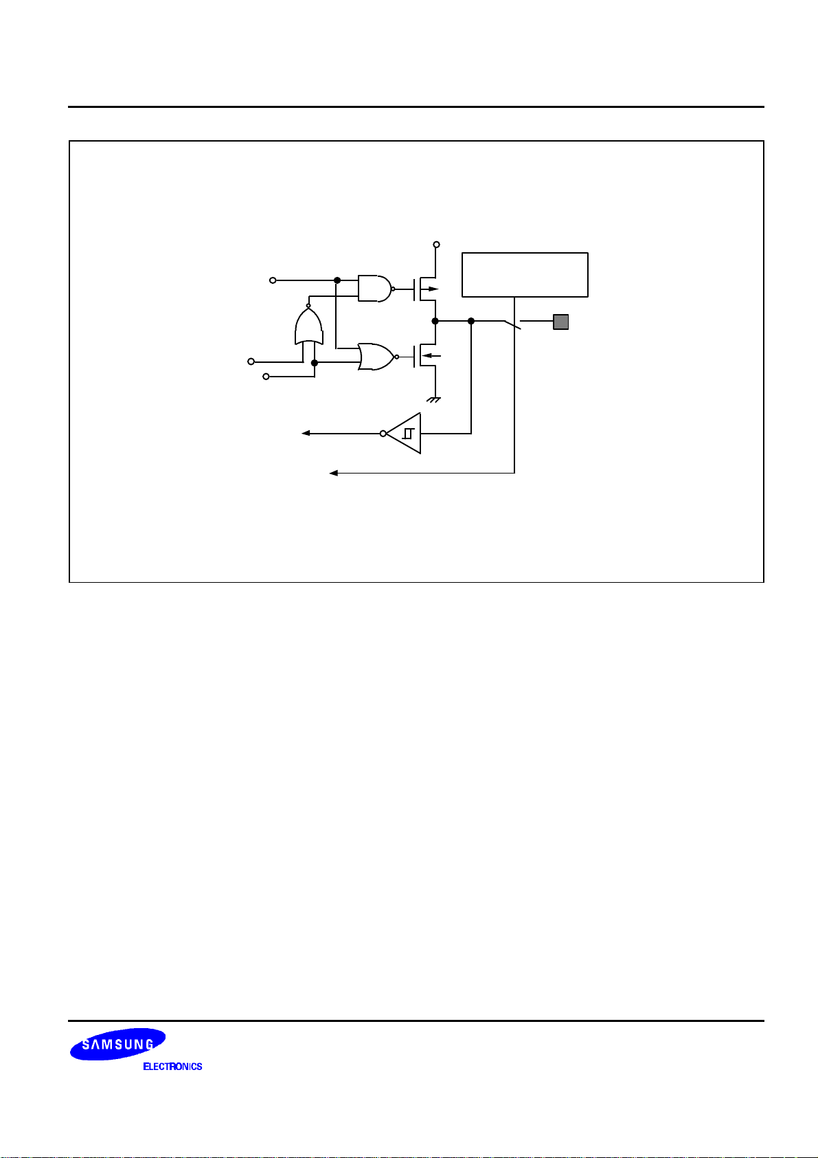
S3C8444 PRODUCT OVERVIEW
V
DD
SELECTION BITS
DATA
OPENDRAIN
OUTPUT
DISABLE
INPUT
OTHER
FUNCTION
V
SS
FOR PORTS OR
OTHER FUNCTIONS
IN / OUT
Figure 1–9. Pin Circuit Type 5 (Port 2, AS, DS, MW, DM, MRAS, DS, MW, DM, MR, PMPM, TA and TB)
1–13
Page 15
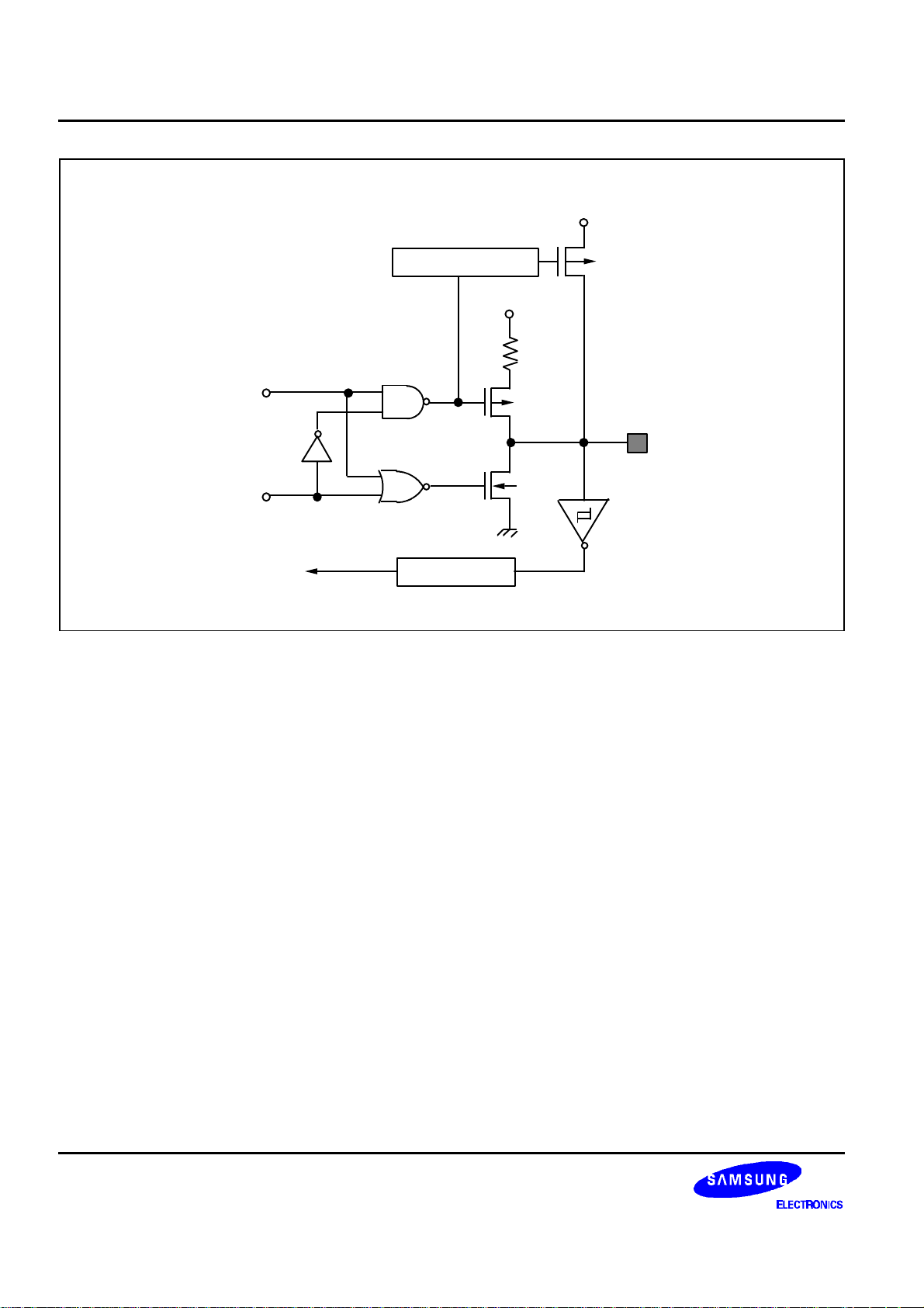
PRODUCT OVERVIEW S3C8444
V
DD
EDGE DETECTION
V
DD
R (46 kΩ)
DATA
IN / OUT
OUTPUT
DISABLE
V
SS
NOISE FILTE RINPUT
a
Figure 1–10. Pin Circuit Type 6 (Serial RxD Pin)
1–14
Page 16
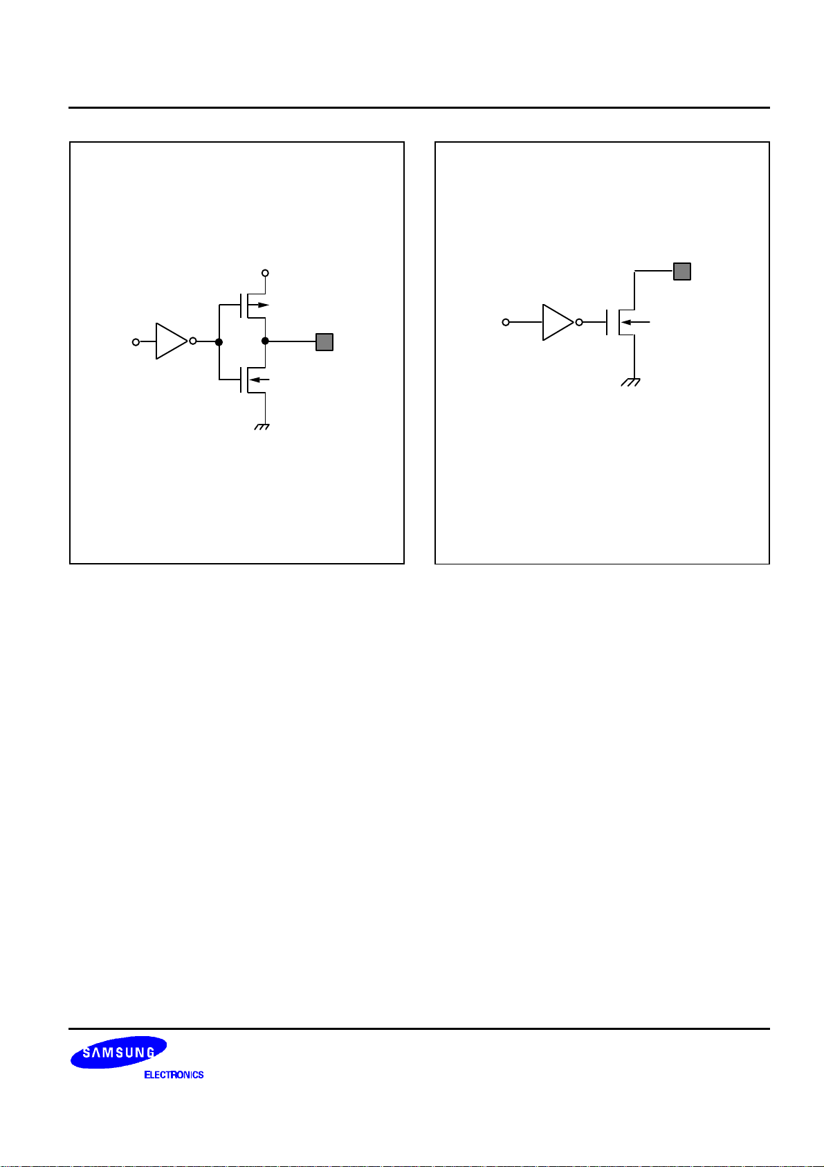
S3C8444 PRODUCT OVERVIEW
V
DD
OUTPUT
DATA
DATA
V
SS
OUTPUT
V
SS
: Circuit type 8 can withstand up to 9-volt loads.
NOTE
Figure 1–11. Pin Circuit Type 7
(AS, serial TxD Pin, PWM0, PWM1)
Figure 1–12. Pin Circuit Type 8 (Port 6)
1–15
Page 17

S3C8444 ELECTRICAL DATA
16 ELECTRICAL DATA
In this section, S3C8444 electrical characteristics are presented in tables and graphs. The information is
arranged in the following order:
— Absolute maximum ratings
— DC electrical characteristics
— AC electrical characteristics
— Input timing for external interrupts (ports 3 and 4)
— Input timing for RESET
— I/O capacitance
— Data retention supply voltage in Stop mode
— Stop mode release timing initiated by RESET
— A./D Converter Electrical Characteristics
— Serial port timing characteristics in mode 0 (10 MHz)
— Serial clock waveform
— Serial port timing in mode 0 (shift register mode)
— External memory timing characteristics (10 MHz)
— External memory read and write timing
— Recommended A/D converter circuit for highest absolute accuracy
— Main oscillator frequency (f
— Main oscillator clock stabilization time (t
— Clock timing measurement at X
— Suboscillator clock stabilization time (t
— Characteristic curves
OSC1
IN
)
)
ST1
)
ST2
16–1
Page 18
ELECTRICAL DATA S3C8444
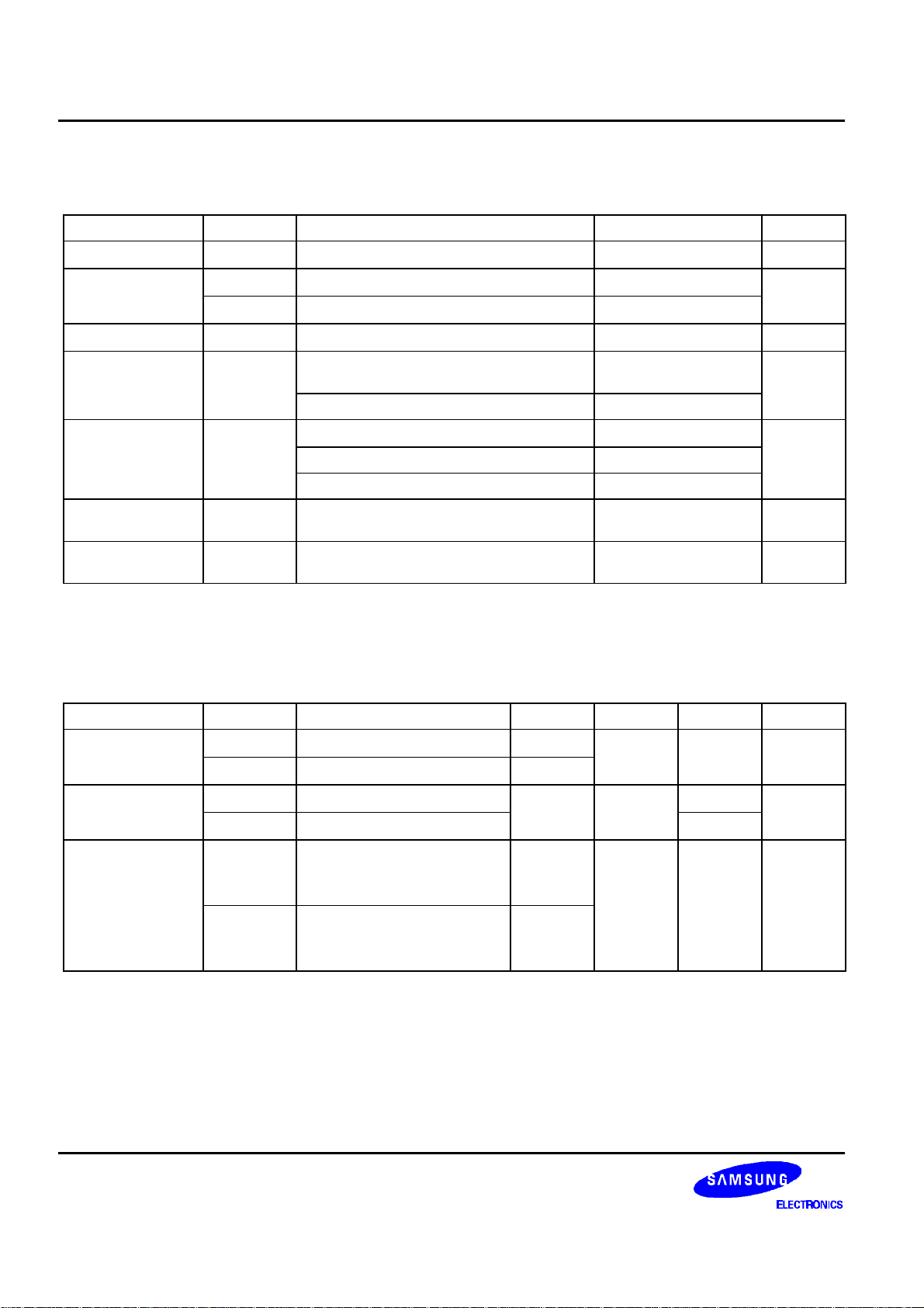
Table 16–1. Absolute Maximum Ratings
(TA = 25°C)
Parameter Symbol Conditions Rating Unit
Supply voltage V
Input voltage V
Output voltage V
Output current
I
DD
V
OH
I1
I2
O
Port 6 only (open-drain) – 0.3 to +10 V
All ports except port 6 – 0.3 to V
One I/O pin active – 18 mA
– 0.3 to +7.0 V
+ 0.3
DD
– 0.3 to VDD + 0.3 V
high
All I/O pins active – 60
Output current low I
OL
One I/O pin active 30 mA
Total pin current for ports 0, 2, 3, 4, 6 100
Total pin current for ports 1 and 5 200
Operating
T
A
– 20 to + 85 °
C
temperature
Storage
T
STG
– 65 to + 150 °
C
temperature
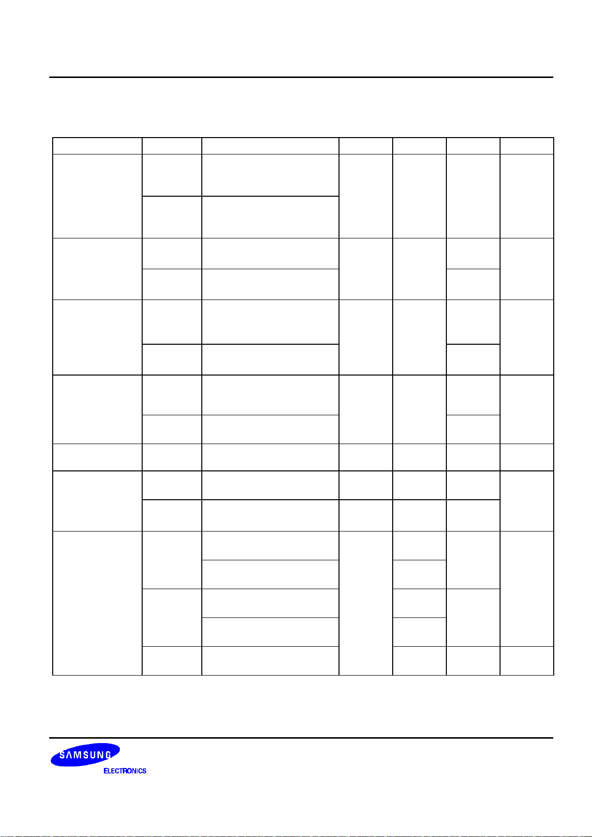
Table 16–2. D.C. Electrical Characteristics
(T
= – 20°C to + 85°C, VDD = 4.5 V to 5.5 V)
A
Parameter Symbol Conditions Min Typ Max Unit
Input high V
voltage V
Input low voltage V
Output high
V
voltage
IH1
IH2
IL1
V
IL2
OH1
All input pins except V
X
IN
All input pins except V
X
IN
VDD = 4.5 V to 5.5 V
IOH = – 1 mA
IH2
IL2
0.8 V
V
DD
DD
– 0.5
– V
DD
– – 0.2 V
0.4
V
– 1.0 – – V
DD
DD
Port 1 only
V
OH2
VDD = 4.5 V to 5.5V
V
DD
– 1.0
IOH = – 200 µA
All output pins except port 1
V
V
16–2
Page 19
S3C8444 ELECTRICAL DATA
Table 16–2. D.C. Electrical Characteristics (Continued)
(T
= – 20°C to + 85°C, VDD = 4.5 V to 5.5 V)
A
Parameter Symbol Conditions Min Typ Max Unit
Output low
voltage
V
OL1
V
= 4.5 V to 5.5 V
DD
IOL = 2 mA
– – 0.4 V
All output pins except port 5
V
OL2
V
= 4.5 V to 5.5 V
DD
IOL = 1.5 mA
Port 5
Input high leakage
current
Input low leakage
current
I
LIH1
I
LIH2
I
LIL1
VIN = V
All input pins except X
VIN = V
X
V
IN
IN
DD
IN
DD
= 0 V
All input pins except XIN,
– – 3 µA
20
– – – 3 µA
and RESET
Output high
leakage current
I
LIL2
I
LOH1
V
= 0 V
IN
X
IN
V
= V
OUT
DD
All output pins except for
– 20
– – 5 µA
port 6
Output low
I
LOH2
I
LOL
Port 6 (open-drain)
V
= 9 V
OUT
V
= 0 V – – – 5 µA
OUT
20
leakage current
Pull-up resistor R
L1
V
IN
= 0 V; V
= 5 V ± 10%
DD
30 46 80
kΩ
Ports 0, 1, 4, 5, and RxD
R
L2
V
IN
= 0 V; V
= 5 V ± 10%
DD
120 230 320
RESET only
Supply current
(1)
I
DD1
V
= 5 V ± 10%
DD
– 35 50 mA
25 MHz crystal oscillator
V
= 5 V ± 10%
DD
30
10 MHz crystal oscillator
I
DD2
Idle mode: VDD = 5 V ± 10%
11 25
25 MHz crystal oscillator
Idle mode: VDD = 5 V ± 10%
5
10 MHz crystal oscillator
I
DD3
Stop mode;
V
= 5 V ± 10%
DD
3 20 µA
NOTE: Supply current does not include current drawn through internal pull-up resistors or external output current loads.
16–3
Page 20
ELECTRICAL DATA S3C8444
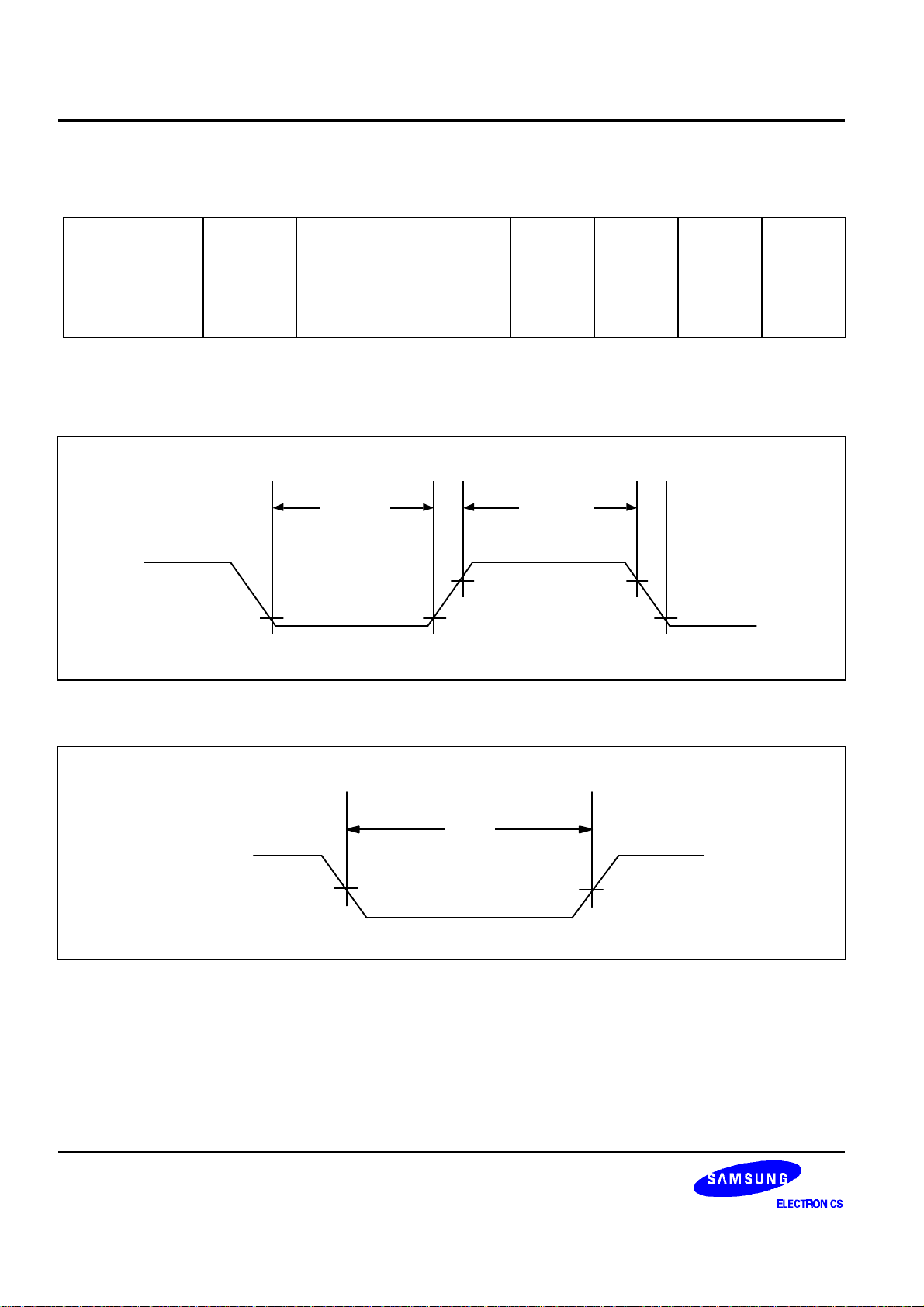
Table 16–3. A.C. Electrical Characteristics
(T
= – 20°C to + 85°C, V
A
= 4.5 V to 6.0V)
DD
Parameter Symbol Conditions Min Typ Max Unit
Interrupt input
high, low width
RESET input low
t
INTH,
t
INTL
t
RSL
P3.0–P3.3, P4.0–P4.7 3 – – t
Input 22 – – t
CPU
CPU
width
NOTES:
1. The unit t
2. The oscillator frequency is the same as CPU clock frequency.
means one CPU clock period.
CPU
t
INTL
0.8 V
0.2 V
DD
DD
t
INTH
Figure 16–1. Input Timing for External Interrupts (Ports 3 and 4)
t
RSL
RESET
0.2 V
DD
16–4
Figure 16–2. Input Timing for RESETRESET
Page 21
S3C8444 ELECTRICAL DATA
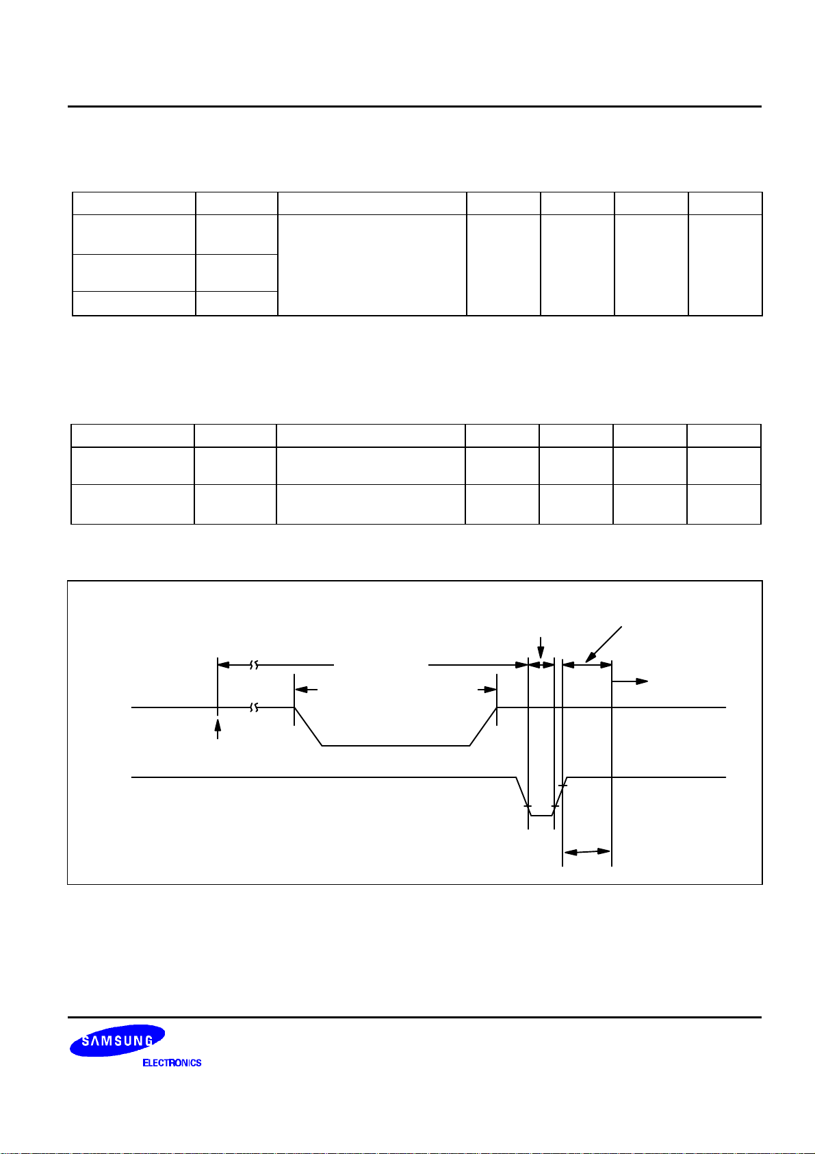
Table 16–4. Input/Output Capacitance
(TA = – 20°C to + 85°C, V
DD
= 0 V )
Parameter Symbol Conditions Min Typ Max Unit
Input
capacitance
Output
C
C
IN
OUT
f = 1 MHz; unmeasured pins
are returned to V
SS
– – 10 pF
capacitance
I/O capacitance C
IO
Table 16–5. Data Retention Supply Voltage in Stop Mode
(TA = – 20°C to + 85°C)
Parameter Symbol Conditions Min Typ Max Unit
Data retention
V
DDDR
2 – 6 V
supply voltage
Data retention
I
DDDR
V
DDDR
= 2 V – – 5 µA
supply current
V
DD
RESET
EXECUTION OF
STOP INSTRUCTION
NOTE
: t
is the same as 4096 x 32 x 1 / f
WAIT
Figure 16–3. Stop Mode Release Timing Initiated by RESETRESET
STOP MODE
DATA RETENTION MODE
V
DDDR
.
OSC
0.2 V
RESET
OCCURS
DD
t
WAIT
OSCILLATION
STABILIZATION
TIME
NORMAL
OPERATING
MODE
16–5
Page 22
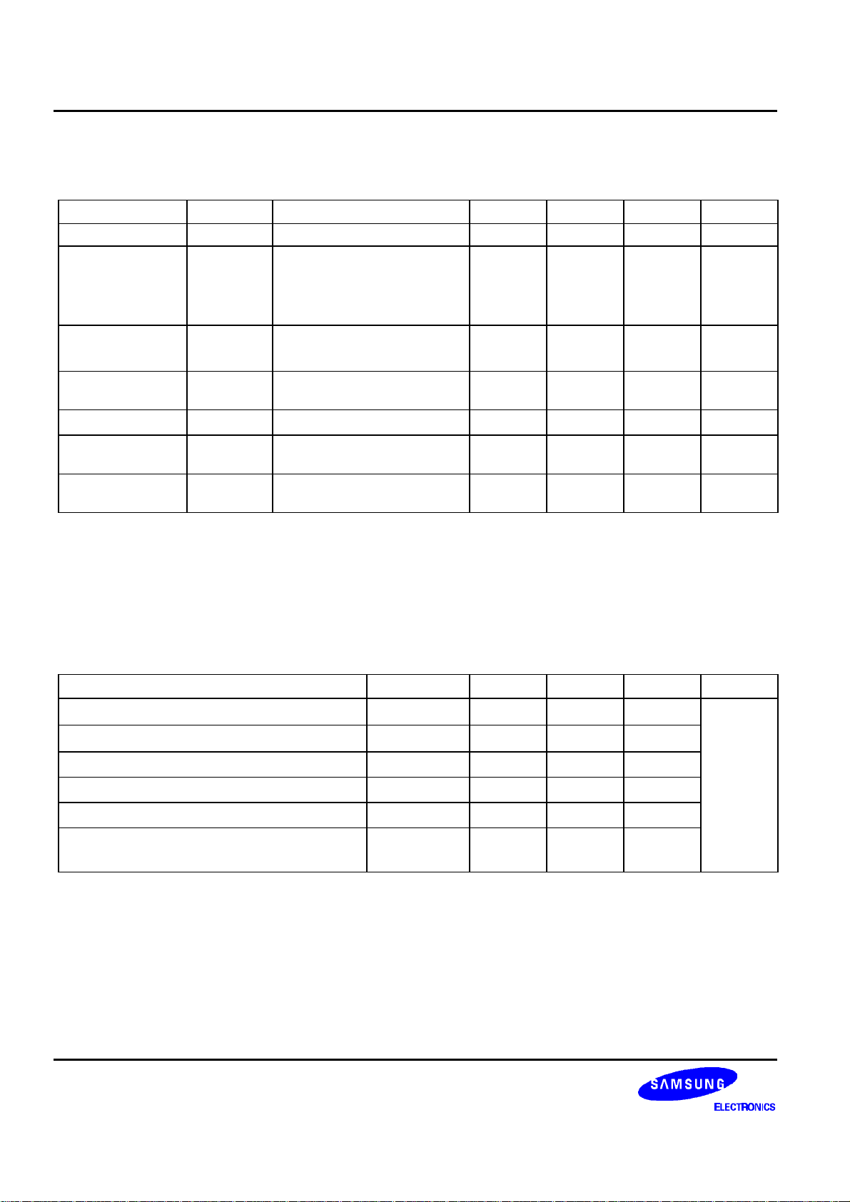
ELECTRICAL DATA S3C8444
Table 16–6. A/D Converter Electrical Characteristics
(T
= – 20°C to + 85°C, VDD = 4.5 V to 6.0 V, VSS = 0 V)
A
Parameter Symbol Conditions Min Typ Max Unit
Resolution 8 8 8 bit
Absolute
accuracy
(1)
VDD = 5.12 V
CPU clock = 18 MHz
AV
= 5.12 V
REF
– – | 3 | LSB
AVSS = 0 V
Conversion
(2)
time
Analog reference
t
AV
CON
REF
t
CPU
192
×
(3)
– – µs
2.56 – V
voltage
Analog ground AV
Analog input
V
SS
IAN
V
AV
SS
SS
– – V
– AV
voltage
Analog input
R
AN
2 – – M½
impedance
NOTES:
1. Excluding quantization error, absolute accuracy equals ± 1/2 LSB.
2. 'Conversion time' is the time required from the moment a conversion operation starts until it ends.
3. t
is the CPU clock period.
CPU
Table 16–7. Serial Port Timing Characteristics in Mode 0 (10 MHz)
(T
= – 20°C to + 85°C, V
A
= 4.5 V to 6.0V, VSS = 0 V)
DD
Parameter Symbol Min Typ Max Unit
Serial port clock cycle time t
Output data setup to clock rising edge t
Clock rising edge to input data valid t
Output data hold after clock rising edge t
Input data hold after clock rising edge t
Serial port clock high, low width t
SCK
S1
S2
H1
H2
HIGH
t
LOW
,
500
300
t
CPU
t
CPU
× 6
× 5
– – 300
50 t
CPU
0 – –
200
t
CPU
× 3
DD
REF
V
V
700 ns
–
–
400
NOTES:
1. All times are in ns and assume a 10 MHz input frequency.
2. The unit t
3. The oscillator frequency is identical to the CPU clock frequency.
means one CPU clock period.
CPU
16–6
Page 23
S3C8444 ELECTRICAL DATA
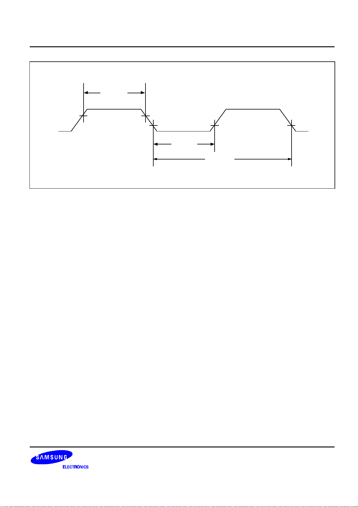
t
HIGH
0.8 V
DD
0.2 V
DD
t
LOW
t
SCK
Figure 16–4. Serial Clock Waveform
16–7
Page 24
ELECTRICAL DATA S3C8444
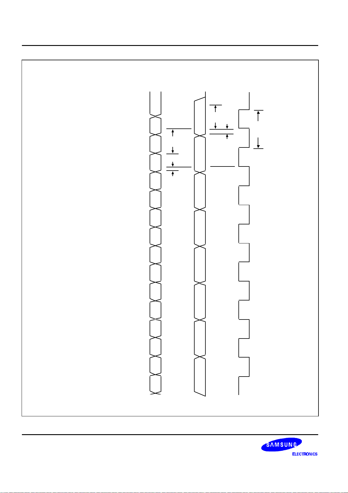
CLOCK
DATA
DATA
OUT
SHIFT
IN
NOTE: The symbols sho
t
t
t
t
t
D0 D1 D2 D3 D4 D5 D6 D7
H2
Output
Clock r
Output
Input d
data hold after clock rising edge
ata hold after clock rising edge
Serial
port clock cycle time
data setup to clock rising edge
ising edge to input data valid
wn in this diagram are defined as follows:
VALID VALID VALID VALID VALID VALID VALID VALID
t
S2
t
H2
t
SCK
S1
S2
H1
S1
t
SCK
t
H1
16–8
Figure 16–5. Serial Port Timing in Mode 0 (Shift Register Mode)
Page 25
S3C8444 ELECTRICAL DATA
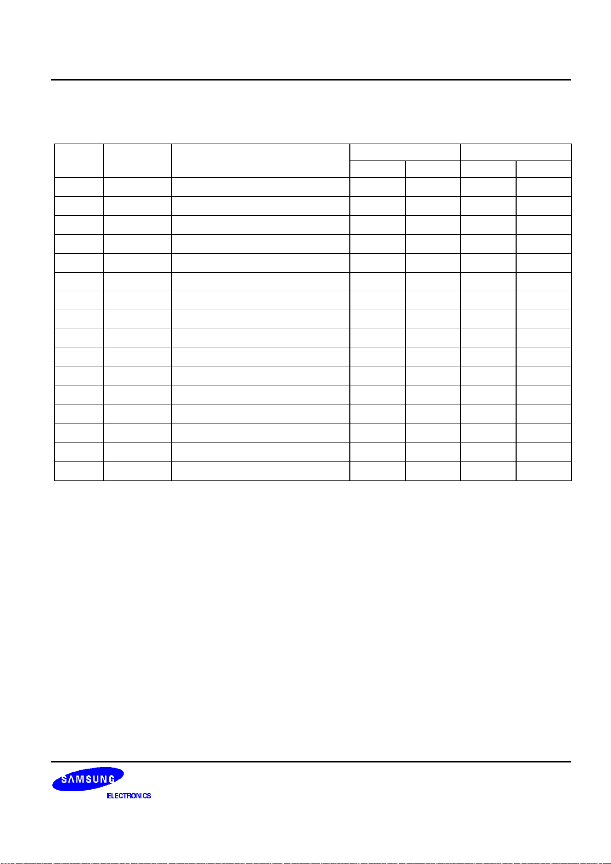
Table 16–8. External Memory Timing Characteristics (10 MHz)
(T
= – 20°C to + 85°C, V
A
= 4.5 V to 6.0 V)
DD
Number Symbol Parameter Normal Timing Extended Timing
Min Max Min Max
1 tdA (AS)
2 t
3 t
4 t
dAS
dAS
wAS
(A)
(DR)
5 tdA (DS)
6a t
6b t
7 t
8 t
9 t
10 t
11 t
12 t
13 t
14 t
15 t
wDS
wDS
dDS
hDS
dDS
dDS
dDO
dAS
hDS
dRW
dDS
(read)
(write)
(DR)
(DR)
(A)
(AS)
(DS)
(W)
(W)
(AS)
(DW)
Address valid to AS ↑ delay
AS ↑ to address float delay
AS ↑ to read data required valid
AS low width
Address float to DS ↓
DS (read) low width
DS (write) low width
DS ↓ to read data required valid
Read data to DS ↑ hold time
DS ↑ to address active delay
DS ↑ to AS ↓ delay
Write data valid to DS (write) ↓ delay
AS ↑ to wait delay
DS ↑ to wait hold time
R/W valid to AS ↑ delay
DS ↑ to write data not valid delay
10 – 50 –
35 – 85 –
– 140 – 335
35 – 85 –
0 – 0 –
125 – 275 –
65 – 165 –
– 80 – 255
0 – 0 –
20 – 70 –
30 – 80 –
10 – 50 –
– 90 – 335
0 – 0 –
20 – 70 –
20 – 70 –
NOTES:
1. All times are in ns and assume a 10 MHz input frequency.
2. Wait states add 100 ns to the time of numbers 3, 6a, 6b, and 7.
3. Auto-wait states add 100 ns to the time of number 12.
16–9
Page 26
ELECTRICAL DATA S3C8444
R/
W
14
PORT A
DM
A8–A15,
3
DM
9
PORT AD D0–D7A0–A7
1 2
AS
4
DS
(P3.7)
WAIT
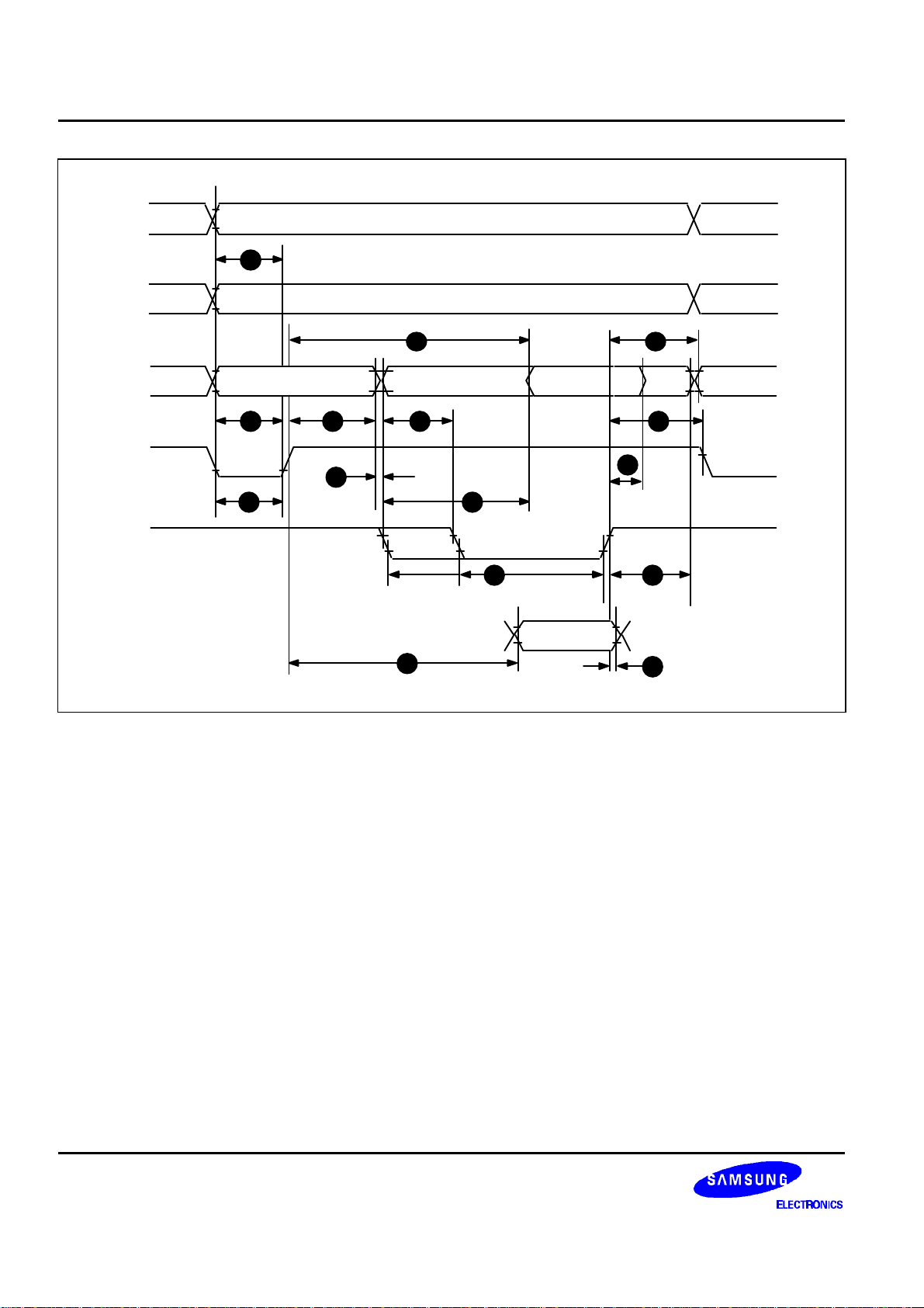
Figure 16–6. External Memory Read and Write Timing
(See Table 15–7 for a description of each timing point.)
IN OUTD0–D7 OUT
1011
5
7
6
WAIT WINDOW
12
8
15
13
16–10
Page 27
S3C8444 ELECTRICAL DATA
V
DD
REFERENCE
VOLTAGE
INPUT
ANALOG
INPUT PIN
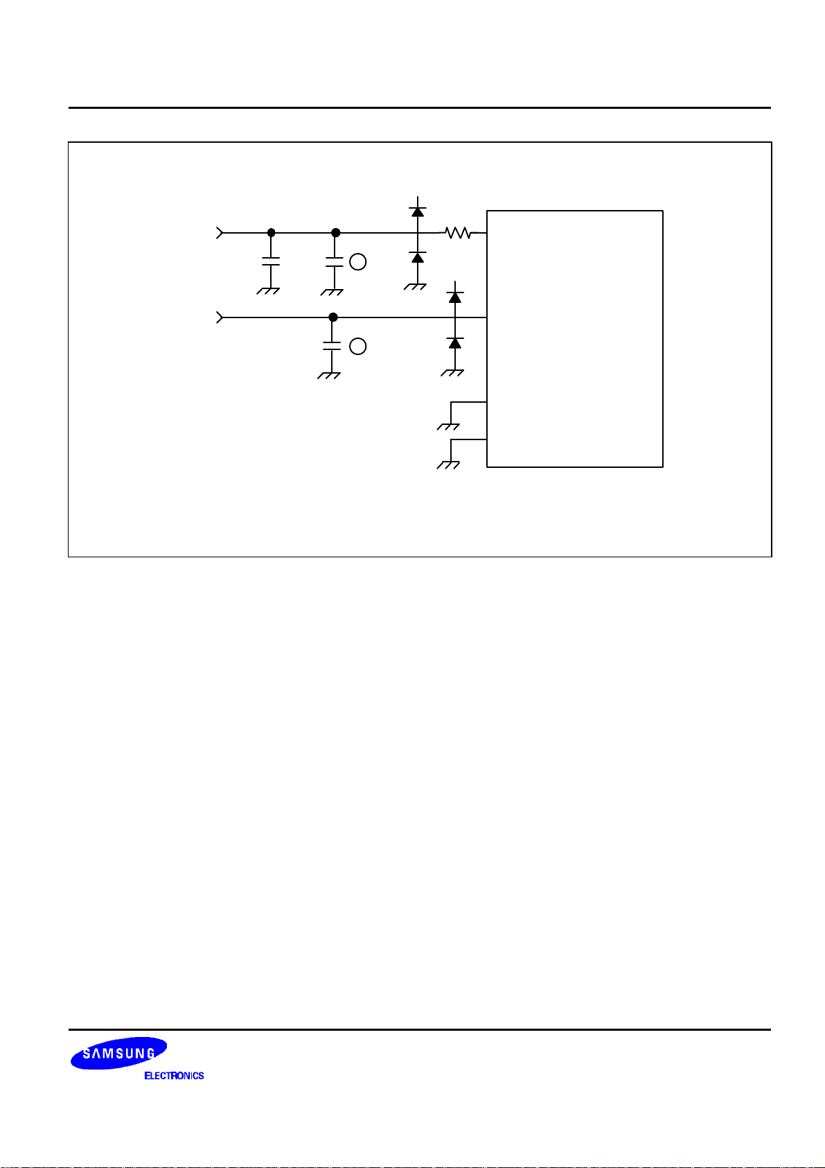
: The symbol 'R' signifies an offset resistor with a value of from 50 to 100 Ohms.
NOTE
Figure 16–7. Recommended A/D Converter Circuit for Highest Absolute Accuracy
10 µF
If this resistor is omitted, the absolute accuracy will be maximum of 4 LSBs.
+
–
C
103
101C
R
AV
REF
V
DD
ADC0–ADC7
S3C8444
AV
SS
V
SS
16–11
Page 28
ELECTRICAL DATA S3C8444
(TA = – 20°C + 85°C, V
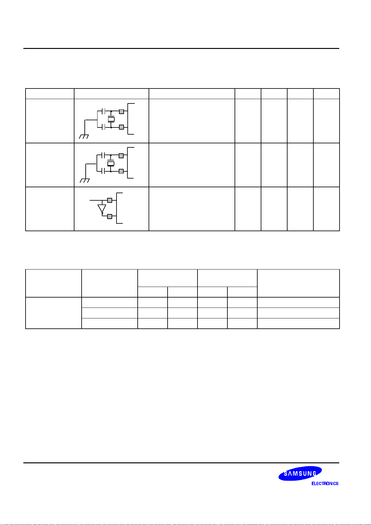
Table 16–9. Main Oscillator Frequency (f
= 4.5 V to 6.0 V)
DD
OSC1
)
Oscillator Clock Circuit Test Condition Min Typ Max Unit
Crystal
Ceramic
External clock
C2
C1
C1
C2
C2
C1
X
X
X
X
X
X
a
X
IN
X
OUT
CPU clock oscillation
frequency
IN
IN
OUT
OUT
CPU clock oscillation
frequency
IN
OUT
1 – 18 MHz
1 – 18 MHz
XIN input frequency 1 – 18 MHz
a
Table 16–10. Recommended Oscillator Constants
(TA = – 20°C + 85°C, VDD = 4.5 V to 6.0 V)
Manufacturer Product Name Load Cap (pF) Oscillator Voltage
Range (V)
C1 C2 MIN MAX
TDK CCR20.0MS6 5 5 4.5 5.5
CCR24.0M6 5 5 4.5 5.5
CCR25.0M6 – 5 4.5 5.5
NOTE: On-chip C: 30pF ±20% built in.
Remarks
SMD Type
SMD Type
SMD Type
16–12
Page 29
S3C8444 ELECTRICAL DATA
Table 16–11. Main Oscillator Clock Stabilization Time (t
ST1
)
(TA = – 20°C + 85°C, VDD = 4.5 V to 6.0 V)
Oscillator Test Condition Min Typ Max Unit
Crystal VDD = 4.5 V to 6.0 V – – 20 ms
Ceramic Stabilization occurs when VDD is equal to the minimum
– – 10 ms
oscillator voltage range.
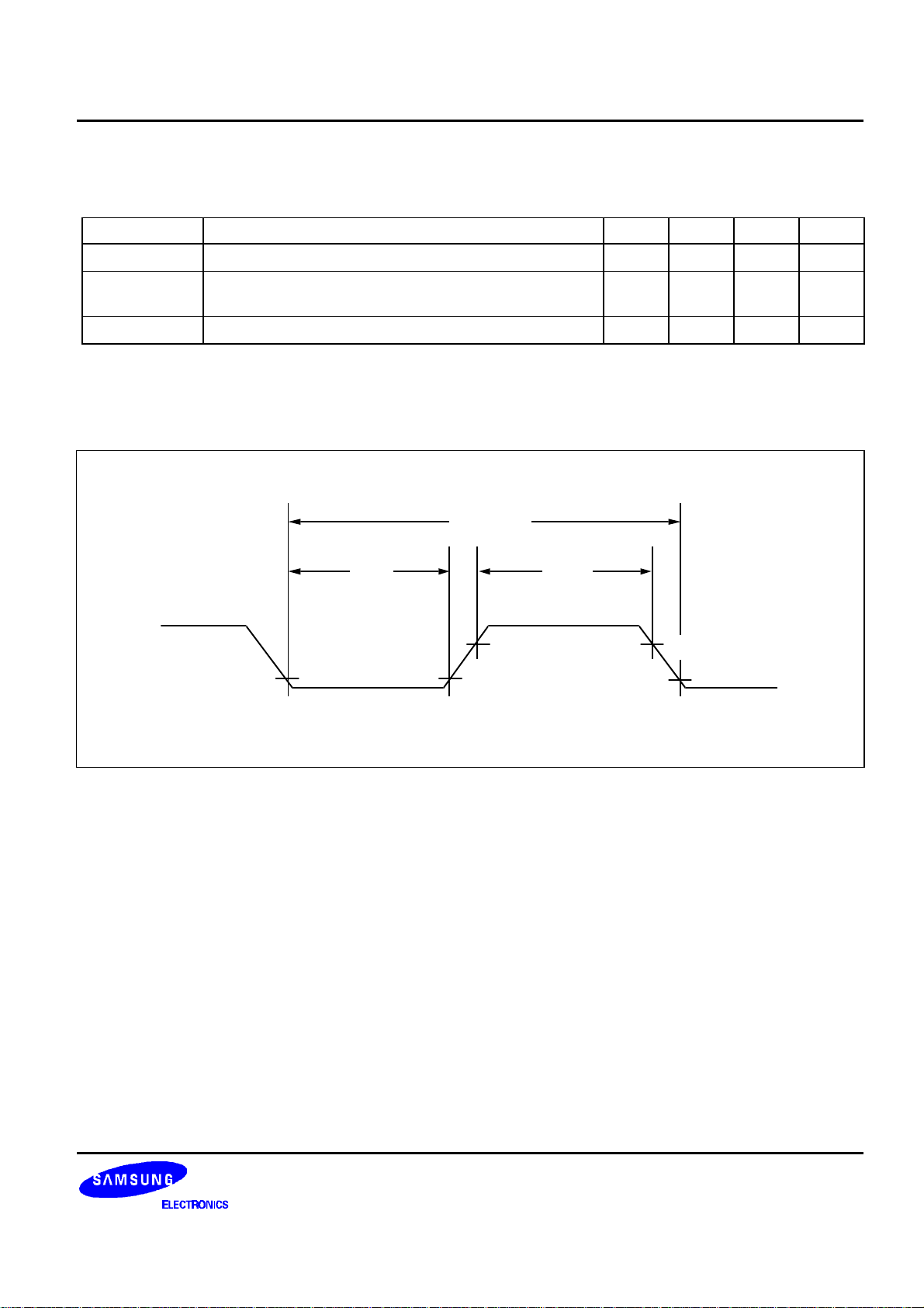
External clock XIN input high and low level width (tXH, tXL) 25 – 500 ns
NOTE: Oscillation stabilization time (t
frequency after a power-on occurs, or when Stop mode is ended by a RESET signal. The RESET should therefore
be held at low level until the t
) is the time required for the CPU clock to return to its normal oscillation
ST1
time has elapsed (see Figure 15–3).
ST1
1 / f
OSC1
t
XL
t
XH
IN
V
DD
X
IN
Figure 16–8. Clock Timing Measurement at X
– 0. 5
0.4 V
V
16–13
Page 30
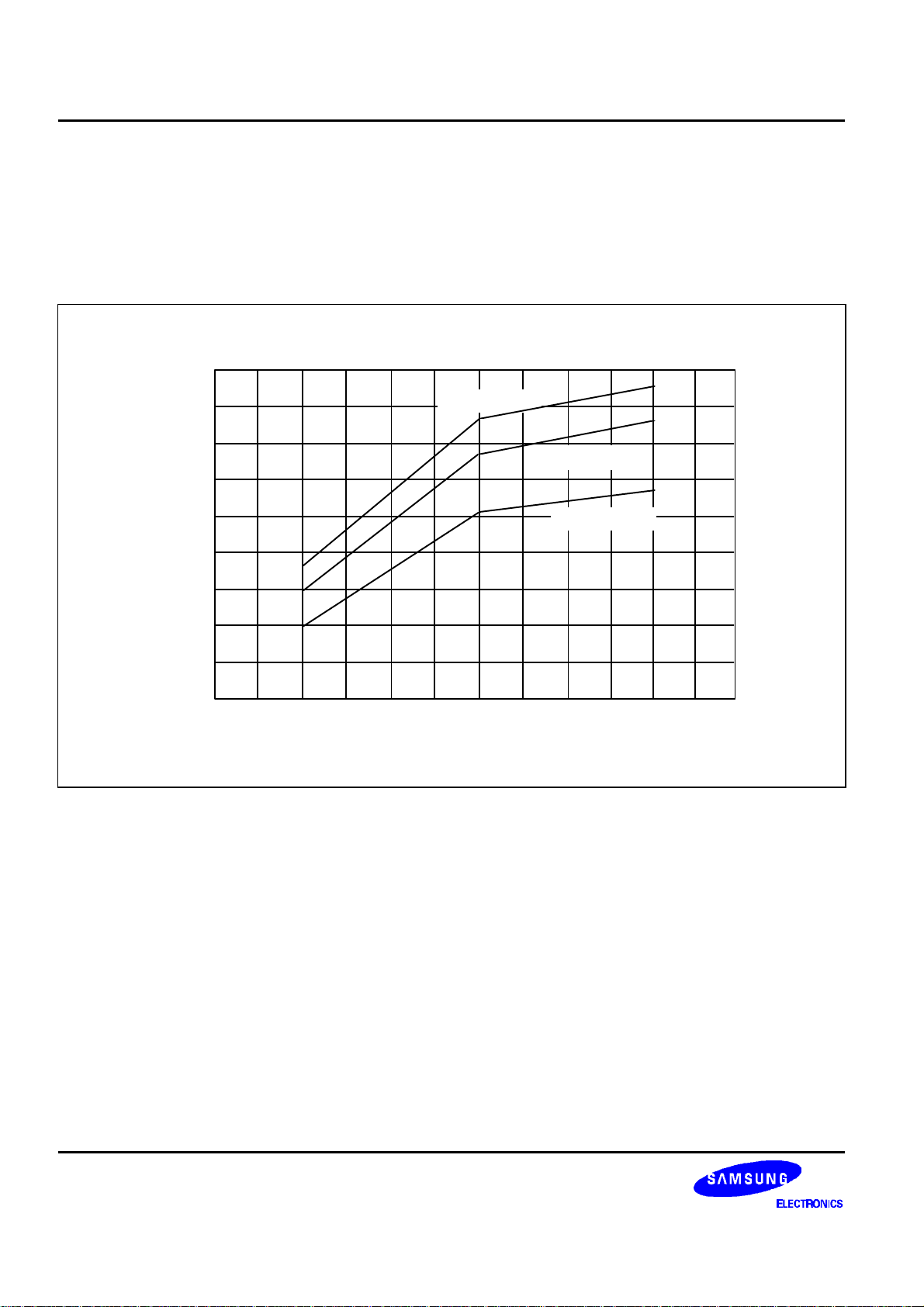
ELECTRICAL DATA S3C8444
CHARACTERISTIC CURVES
NOTE
The characteristic values shown in the following graphs are based on actual test measurements. They do
not, however, represent guaranteed operating values.
(TA = 25 °C)
38
f
= 25 MHz
36
OSC
34
32
(mA)
30
DD1
I
28
26
24
22
4.5
5.0 5.5
VDD (V)
Figure 16–9. IDD1 vs VDD
f
OSC
f
OSC
= 20 MHz
= 10 MHz
16–14
Page 31
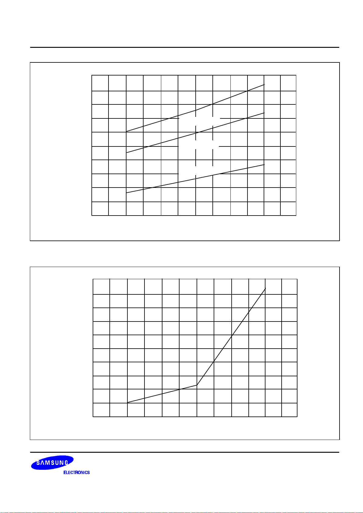
S3C8444 ELECTRICAL DATA
(TA = 25 °C)
13
12
11
10
9
(mA)
8
DD2
I
7
6
5
4
280
4.5
(TA = 25 °C)
f
= 25 MHz
OSC
f
= 20 MHz
OSC
f
= 10 MHz
OSC
5.0 5.5
VDD (V)
Figure 16–10. IDD2 vs VDD
260
240
220
200
(nA)
DD3
180
I
160
140
120
100
4.5
5.0 5.5
VDD (V)
Figure 16–11. IDD3 vs VDD
16–15
Page 32
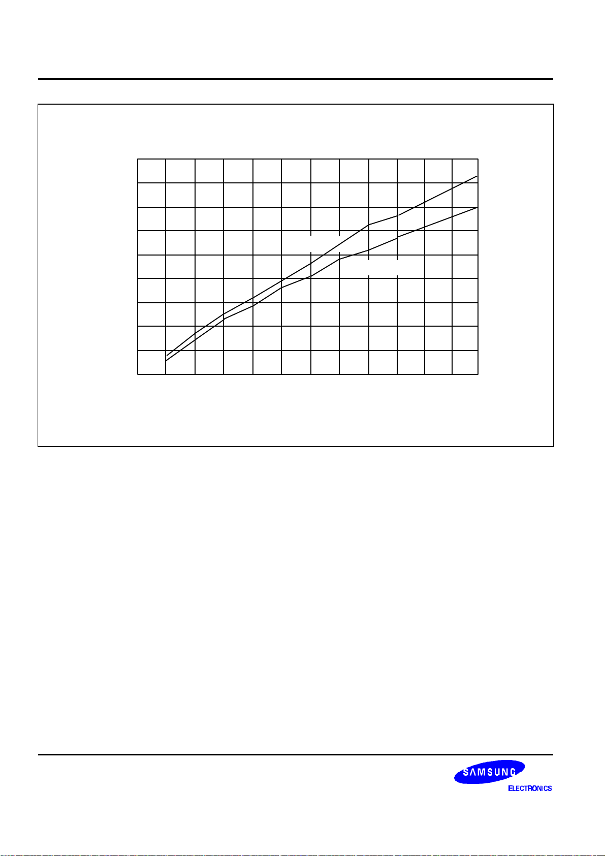
ELECTRICAL DATA S3C8444
(TA = 25 °C)
18
16
14
12
(mA)
OL
10
I
8
6
4
2
VDD = 5.5 V
VDD = 4.5 V
0
0.2
0.4
V
0.6 0.8 1.0
(V)
OL1
1.2
Figure 16–12. IOL vs VOL1
16–16
Page 33
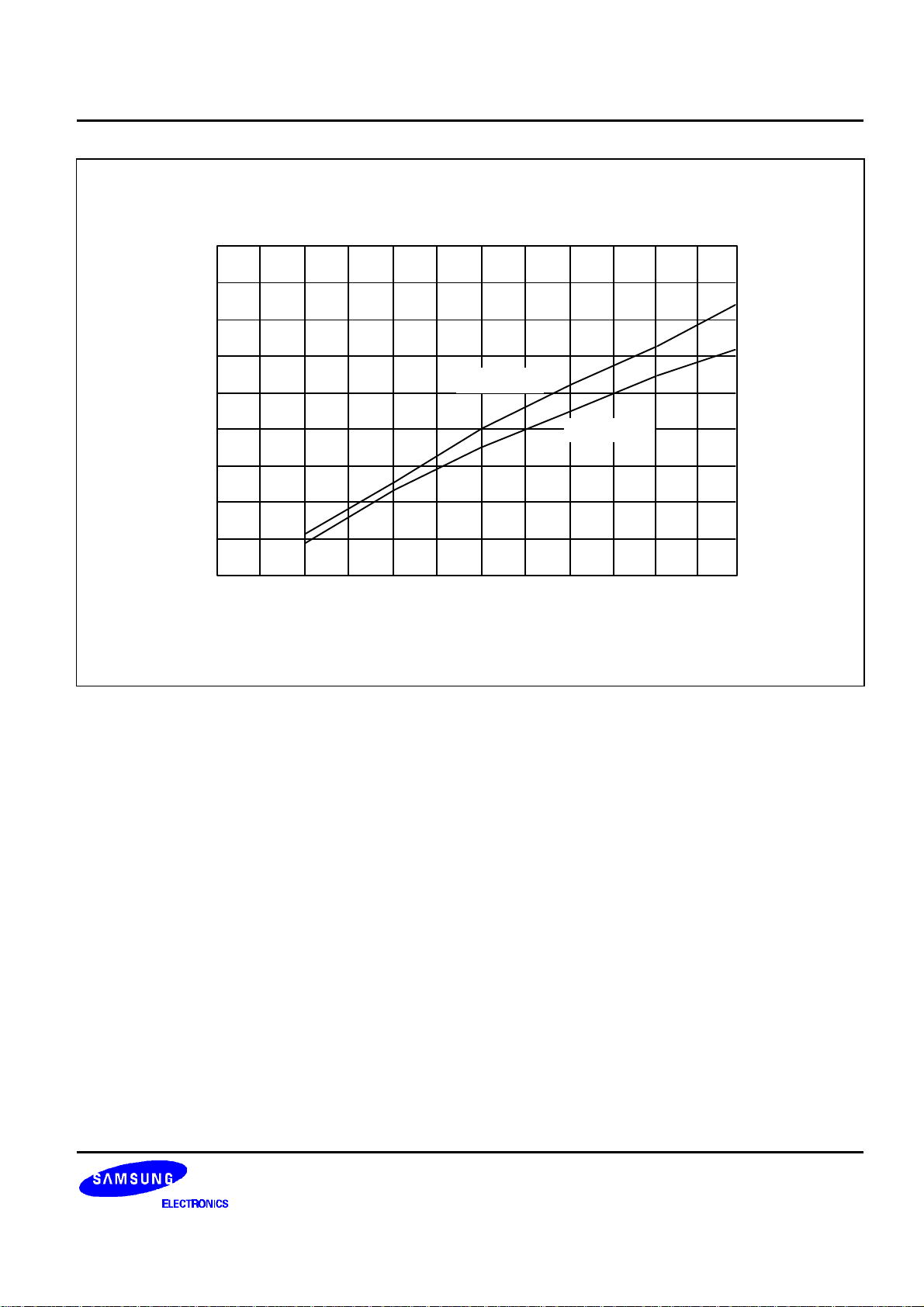
S3C8444 ELECTRICAL DATA
(TA = 25 °C)
18
16
14
12
(mA)
OL
10
I
8
6
4
2
VDD = 5.5 V
VDD = 4.5 V
0
0.2
0.4
V
0.6 0.8 1.0
(V)
OL2
1.2
Figure 16–13. IOL vs VOL2
16–17
Page 34
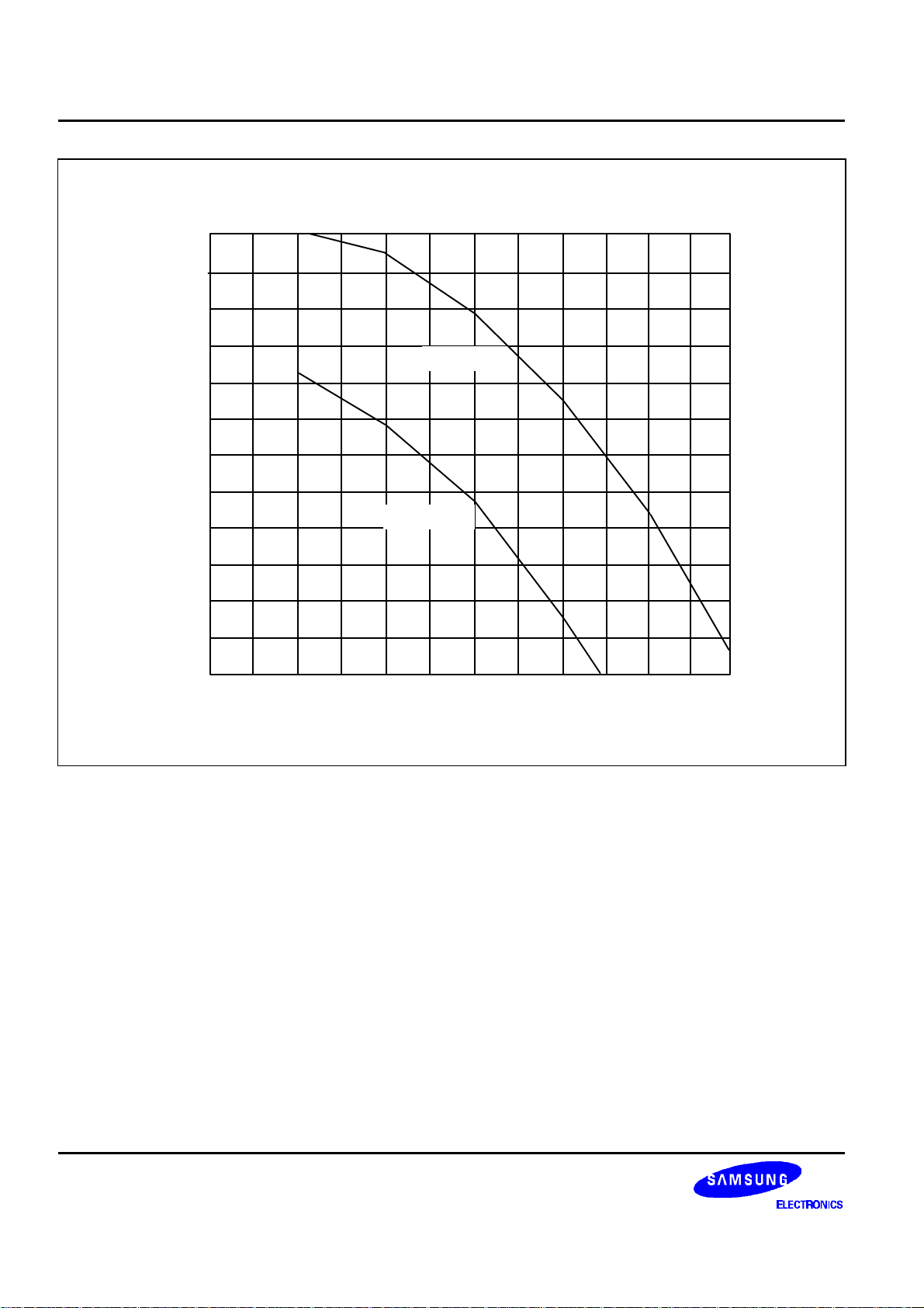
ELECTRICAL DATA S3C8444
(TA = 25 °C)
-12
-11
-10
-9
-8
-7
-6
(mA)
OH
-5
I
-4
-3
-2
-1
0
2.4
VDD = 5.5 V
VDD = 4.5 V
3.0
3.6 4.2 4.8
V
(V)
OH2
Figure 16–14. IOH vs VOH2
5.4
16–18
Page 35
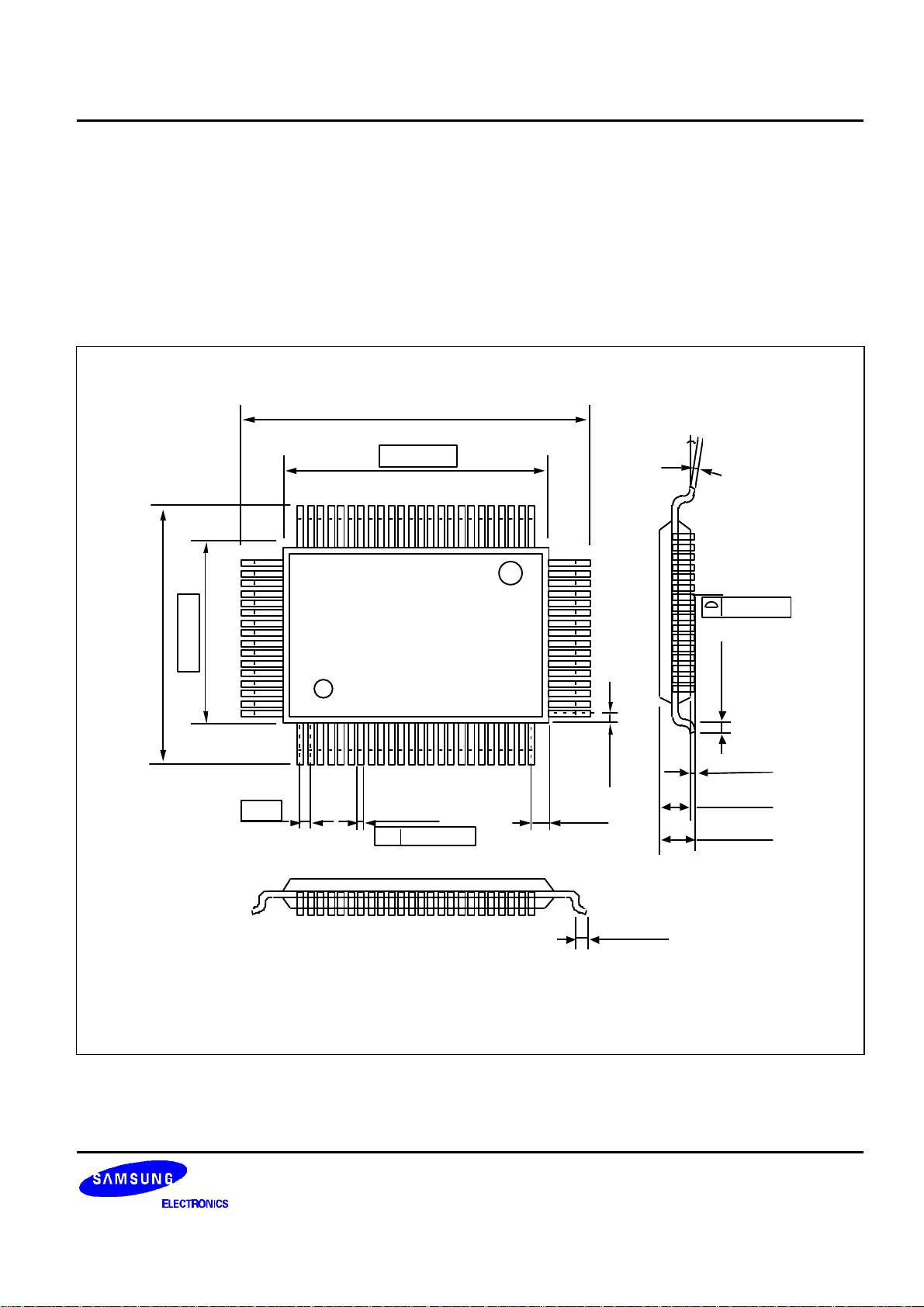
S3C8444 MECHANICAL DATA
17 MECHANICAL DATA
23.90
± 0.3
17.90 ± 0.3
14.00 ± 0.2
#80
0.80
#1
20.00
± 0.2
80-QFP-1420C
0.35
± 0.1
± 0.15 MAX
(0.80)
(1.00)
0~8°
0.15
0.10 MAX
0.80 ± 0.20
0.05 MIN
2.65
± 0.10
3.00 MAX
+0.10
- 0.05
0.80
± 0.20
: Dimensions are in millimeters.
NOTE
Figure 17–1. S3C8444 QFP Standard Package Dimensions (in Millimeters)
17–1
Page 36
MECHANICAL DATA S3C8444
14.00BSC
12.00BSC
0BSC
14.0
12.00BSC
#80
#1
0.50
80-TQFP-1212-AN
0.17~0.27
± 0.08 MAX M
(1.25)
0~7°
0.09~0.20
0.10 MAX
0.65 ± 0.15
0.25GAUGE PLANE
0.05~0.15
± 0.05
1.00
1.20 MAX
17–2
NOTE
: Dimensions are in millimeters.
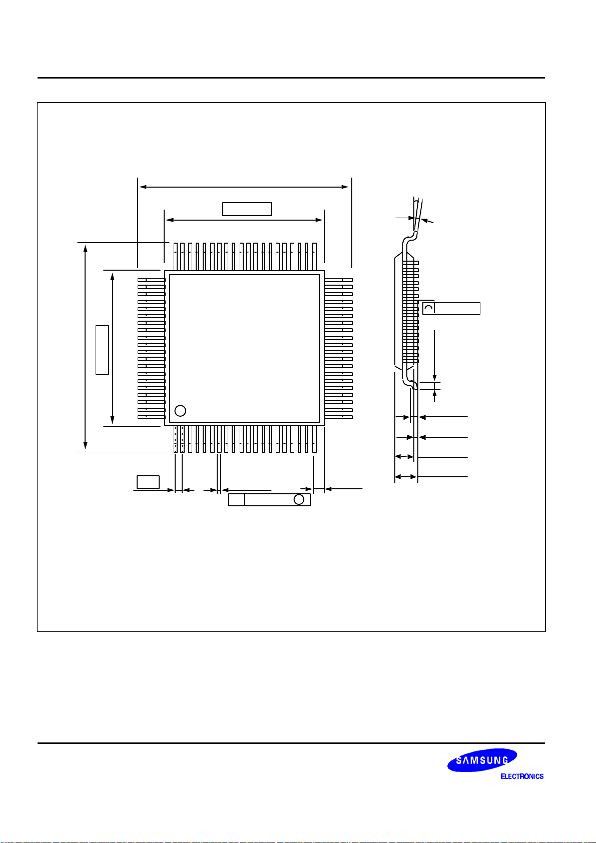
Figure 17–2. S3C8444 TQFP Standard Package Dimensions (in Millimeters)
Page 37

S3C8444 DEVELOPMENT TOOLS
18 DEVELOPMENT TOOLS
OVERVIEW
Samsung provides a powerful and easy-to-use development support system in turnkey form. The development
support system is configured with a host system, debugging tools, and support software. For the host system, any
standard computer that operates with MS-DOS as its operating system can be used. Two types of debugging
tools including hardware and software are provided: the in-circuit emulator, SMDS2, developed for S3C1, S3C7,
S3C8 families of microcontrollers, and even more sophisticated and powerful in-circuit emulator, SMDS2+, for
S3C7, S3C8 families of microcontrollers. The SMDS2+ is a new and improved version of SMDS2. In the future
SMDS2+ will replace SMDS2 and eventually SMDS2 will not be supported. Samsung also offers support
software that includes debugger, assembler, and a program for setting options.
DEVELOPMENT TOOLS VERSIONS
As of the date of this publication, two versions of the SMDS are being supported:
— SMDS2 Version 5.3 (S/W) and SMDS2 Version 1.3 (H/W); last release: October, 1995.
— SHINE Version 1.0 (S/W) and SMDS2+ Version 1.0 (H/W); last release: January, 1997.
SMDS V5.3
SMDS V5.3 is an assembly level debugger with user-friendly host interfacing that uses in-circuit
emulator,SMDS2.
SHINE
Samsung Host Interface for iN-circuit Emulator, SHINE, is a multi-window based debugger for SMDS2+. SHINE
provides pull-down and pop-up menus, mouse support, function/hot keys, and context-sensitive hyper-linked
help. It has an advanced, multiple-windowed user interface that emphasizes ease of use. Each window can be
sized, moved, scrolled, highlighted, added, or removed completely.
SAMA ASSEMBLER
The Samsung Arrangeable Microcontroller (SAM) Assembler, SAMA, is a universal assembler, and generates
object code in standard hexadecimal format. Assembled program code includes the object code that is used for
ROM data and required SMDS program control data. To assemble programs, SAMA requires a source file and
an auxiliary definition (DEF) file with device specific information.
SASM88
The SASM88 is an relocatable assembler for Samsung's S3C8-series microcontrollers. The SASM88 takes a
source file containing assembly language statements and translates into a corresponding source code, object
code and comments. The SASM88 supports macros and conditional assembly. It runs on the MS-DOS operating
system. It produces the relocatable object code only, so the user should link object file. Object files can be linked
with other object files and loaded into memory.
18–1
Page 38
DEVELOPMENT TOOLS S3C8444
HEX2ROM
HEX2ROM file generates ROM code from HEX file which has been produced by assembler. ROM code must be
needed to fabricate a microcontroller which has a mask ROM. When generating the ROM code (.OBJ file) by
HEX2ROM, the value 'FF' is filled into the unused ROM area upto the maximum ROM size of the target device
automatically.
TARGET BOARDS
Target boards are available for all S3C8-series microcontrollers. All required target system cables and adapters
are included with the device-specific target board.
IBM-PC AT
or
Compatible
RS-232C
5-Volt
Power
Supply
Front
Panel
Board
Target
Application
System
Internal BUS
Main Board
Personality
Board
POD
TB8444
Target
Board
18–2
Target Cable
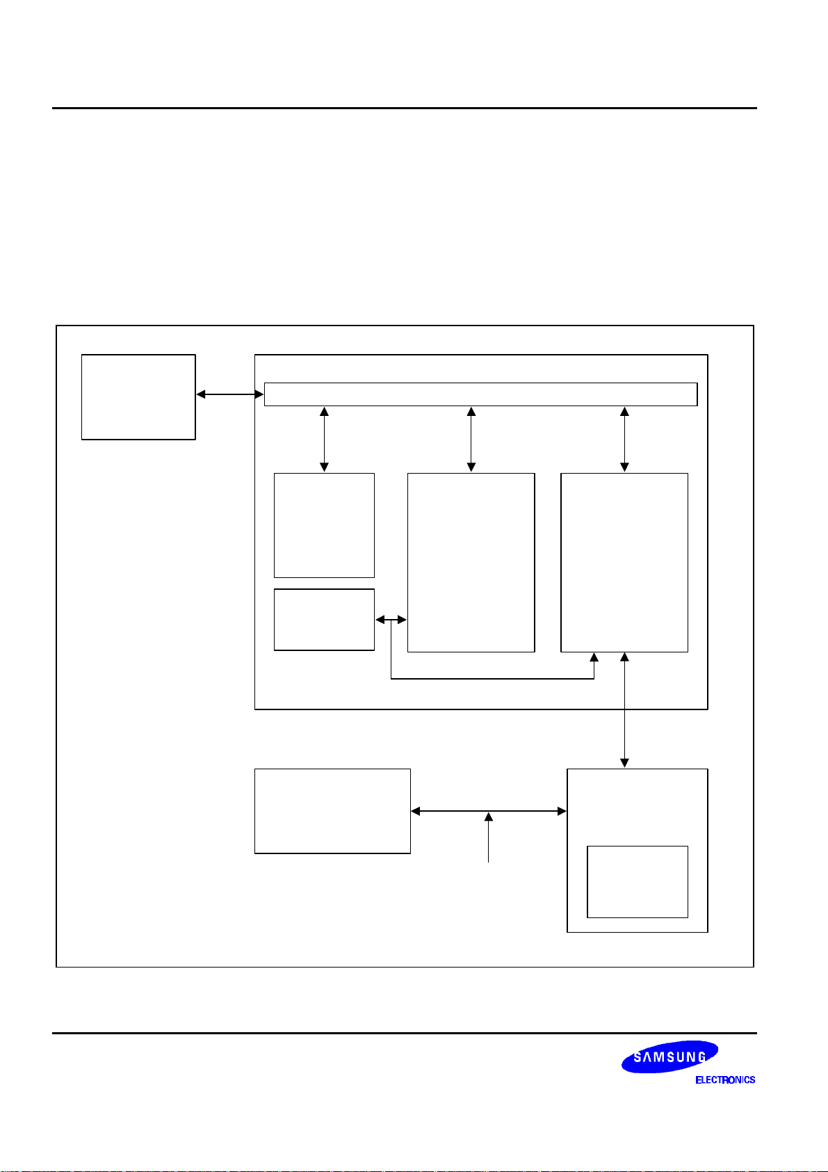
Figure 18–1. SMDS Product Configuration (SMDS2)
EVA
Chip
Page 39
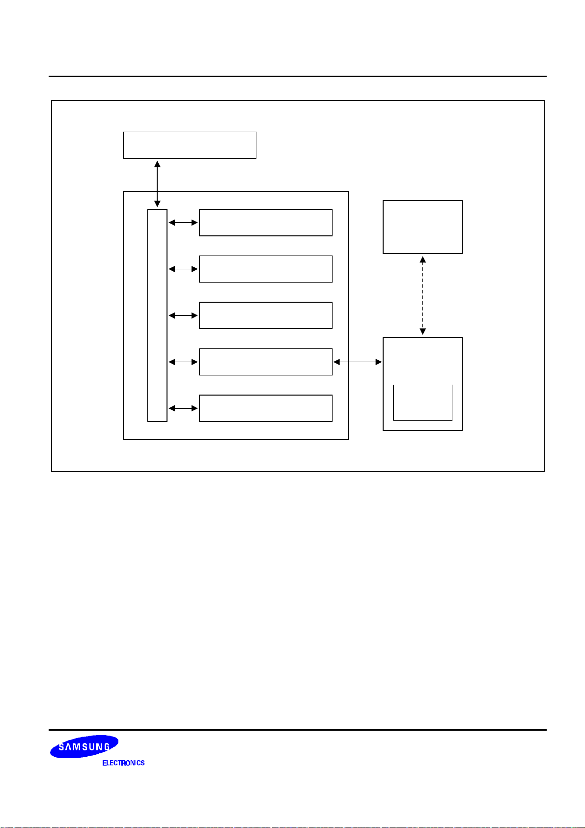
S3C8444 DEVELOPMENT TOOLS
IBM-PC AT or Compatible
SMDS2+RS-232C
PROM/MTP Writer Unit
RAM Break/Display Unit
Bus
Trace/Timer Unit
SAM8 Base Unit
Power Supply Unit
POD
Figure 18–2. SMDS Product Configuration (SMDS2+)
Target
Application
System
Target
Cable
TB8444
Target
Board
EVA
Chip
18–3
Page 40
DEVELOPMENT TOOLS S3C8444
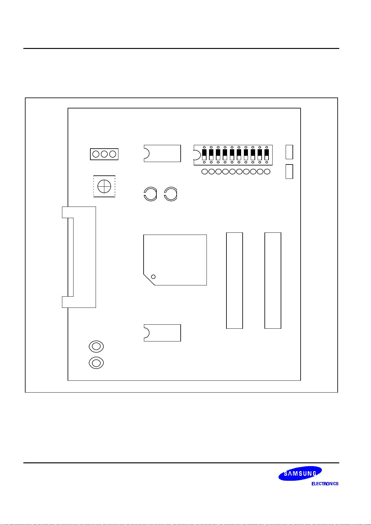
40-Pin Connector
TB8444 TARGET BOARD
The TB8444 target board is used for the S3C8444 microcontroller. It is supported by the SMDS2 or SMDS2+
development system.
TB8444
To User_VCC
Off On
RESET1
25
CN1
1
External
Triggers
CH1
Stop+Idle
+
U3 U1
144 QFP
S3E8440
EVA Chip
SW1
P7.7
P7.6
AVSS
39 40
P7.5
P7.4
P7.3
P7.2
P7.1
J101
21
40-Pin Connector
GND VCC
P7.0
AVREF
J102
21
39 40
18–4
CH2
SM1296A
Figure 18–3. TB8444Target Board Configuration
Page 41
S3C8444 DEVELOPMENT TOOLS
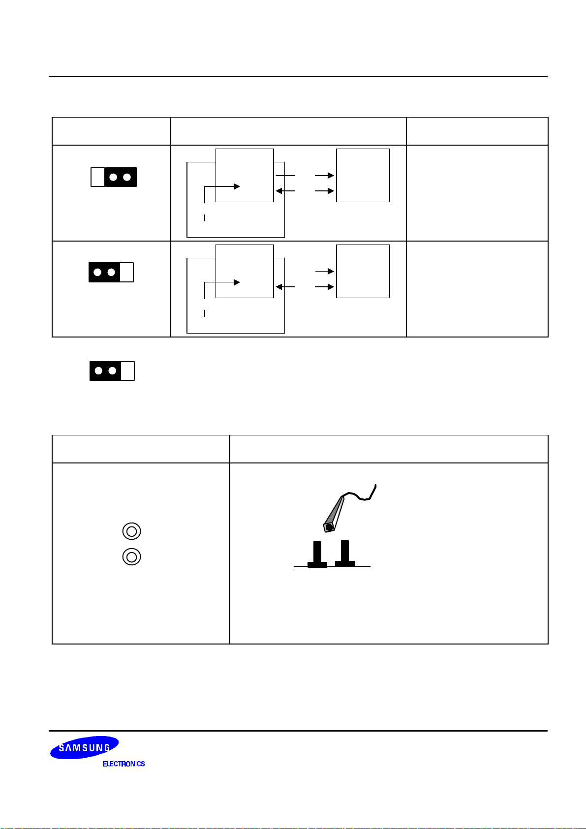
Table 18–1. Power Selection Settings for TB8444
'To User_Vcc' Settings Operating Mode Comments
To User_Vcc
OFF ON
a
To User_Vcc
OFF ON
a
TB8444
VCC
SMDS2/SMDS2+
TB8444
VCC
VSS
External
VCC
VSS
Target
System
Target
System
The SMDS2/SMDS2+ main
board supplies VCC to the
target board (evaluation chip)
and the target system.
The SMDS2/SMDS2+ main
board supplies VCC only to
the target board (evaluation
chip). The target system must
have its own power supply.
VCC
SMDS2/SMDS2+
NOTE: The following symbol in the 'To User_Vcc' Setting column indicates the electrical short configuration:
a
Table 18–2. Using Single Header Pins as the Input Path for External Trigger Sources
Target Board Part Comments
Connector from
EXTERNAL
TRIGGERS
external trigger
sources of the
application system
CH1
CH2
You can connect an external trigger source to one of the two external
trigger channels (CH1 or CH2) for the SMDS2/SMDS2+ breakpoint
and trace functions.
18–5
Page 42
DEVELOPMENT TOOLS S3C8444
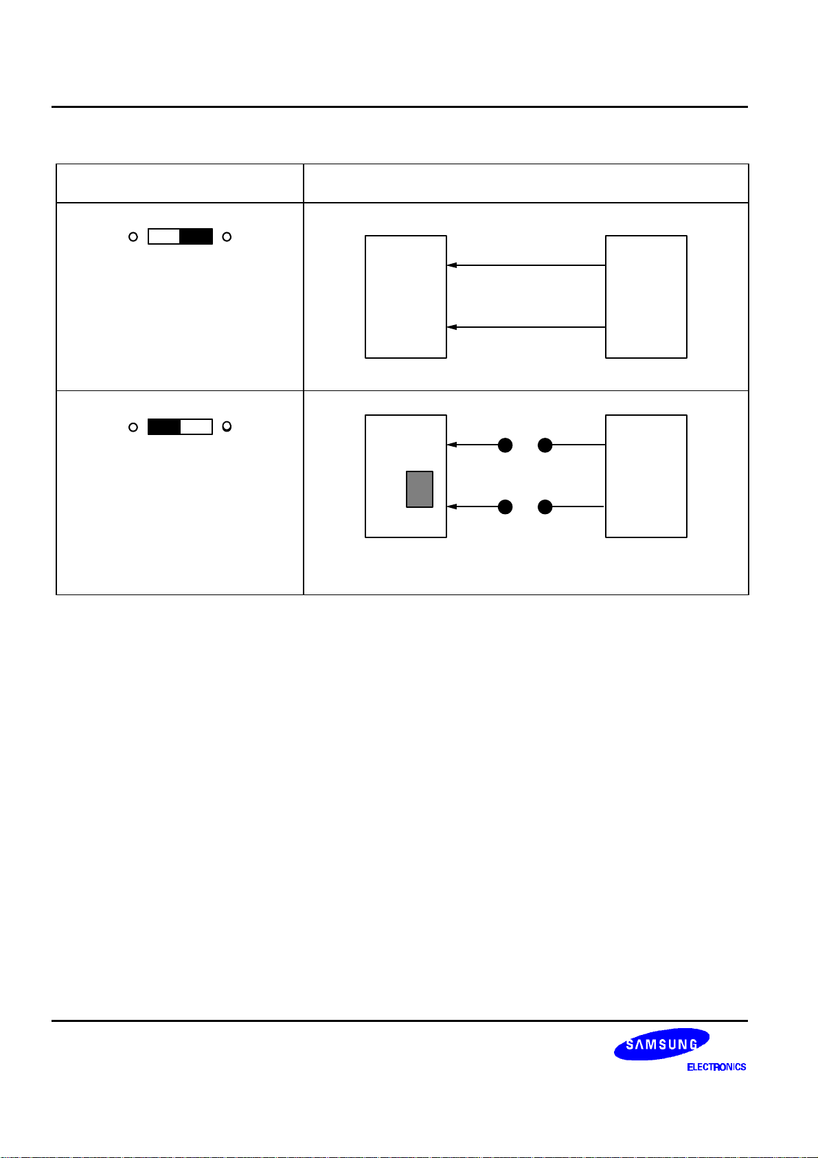
Table 18–3. Analog Pin Connection Switch Settings (TB8444)
Analog Pin Switch Operating Mode
DIP SW1: ON
ANALOG SIGNALS
TARGET
BOARD
•
•
•
TARGET
SYSTEM
DIP SW1: OFF
TARGET
BOARD
ADC0
|
ADC7
NOTE: Analog signals coming into the target board can easily introduce noise into the analog converter circuit. This can
cause invalid conversion results. To reduce noise, you can use the analog pin switches to provide the shortest
possible path for analog signals. To do this, turn all DIP switches to the OFF position. Then, connect the analog
signal lines directly via the holes of the corresponding analog pins.
•
•
•
HOLES DRILLED
FOR DIRECT CONNECTION
•
•
•
TARGET
SYSTEM
IDLE LED
The Green LED is ON when the evaluation chip(S3E8440) is in idle mode.
STOP LED
The Red LED is ON when the evaluation chip(S3E8440) is in stop mode.
18–6
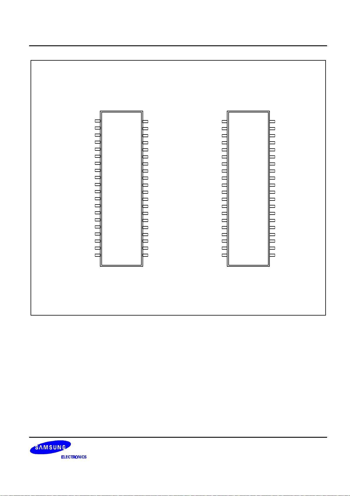
Page 43
S3C8444 DEVELOPMENT TOOLS
A9
P5.7
P5.5
P5.3
P5.1
VDD2
P2.6/TA
DR
DW
AS
TXD
PWM0
P3.1/TDCK/INT1
P3.3/TDG/INT3
P3.5
WAIT
P3.7/
P4.0/INT4
P4.2/INT6
P4.4/INT8
P4.6/INT10
J101
1
3
5
7
9
40-PIN CONNECTOR
11
13
15
17
19
21
23
25
27
29
31
33
35
37
39
2
A8
4
P5.6
6
P5.4
8
P5.2
10
P5.0
12
P2.7/TB
14
PM
16
DM
18
DS
20
PXD
22
PWM1
24
P3.0/TCCK/INT0
26
P3.2/TCG/INT2
28
P3.4
30
P3.6/CAP
32
VSS2
34
P4.1/INT5
36
P4.3/INT7
38
P4.5/INT9
40
P4.7/INT11
P7.0/ADC0
P7.1/ADC1
AVSS
P7.4/ADC4
P7.6/ADC6
P6.7
P6.5
P6.3
P6.1
NC(XIN)
V
SS1
NC
EA
AD6
AD4
AD2
AD0
A15
A13
A11
J102
41
43
45
47
49
51
53
55
57
59
61
63
65
67
69
71
73
75
77
79
42
44
46
48
50
40-PIN CONNECTOR
52
54
56
58
60
62
64
66
68
70
72
74
76
78
80
AV
REF
P7.2/ADC2
P7.3/ADC3
P7.5/ADC5
P7.7/ADC7
P6.6
P6.4
P6.2
P6.0
NC(X
OUT
NC
RESET
AD7
AD5
AD3
AD1
V
DD1
A14
A12
A10
)
Figure 18–4. 40-Pin Connectors for TB8444 (S3C8444, 80-QFP Package)
18–7
Page 44
DEVELOPMENT TOOLS S3C8444
TARGET BOARD TARGET SYSTEM
40-PIN CONNECTORS
J101 J102
1 2
41 42
80-QFP Adapter
Order Code: SM6402
Target Cable for 80 QFP Adapter
Part Name: CS80QF
Order Code: SM6501
40
39
7980
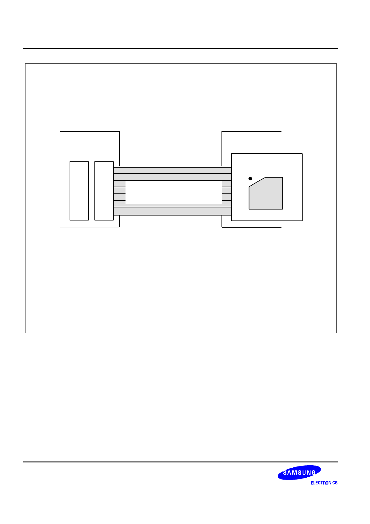
: Two 40-pin flat cables can be used instead of the target cable and the 80-QFP adapter
NOTE
to connect the target board and the target system.
Figure 18–5. TB8444 Cable for 80-QFP Adapter
18–8
 Loading...