

Page 1

S3C7544/P7544 PRODUCT OVERVIEW
1 PRODUCT OVERVIEW
OVERVIEW
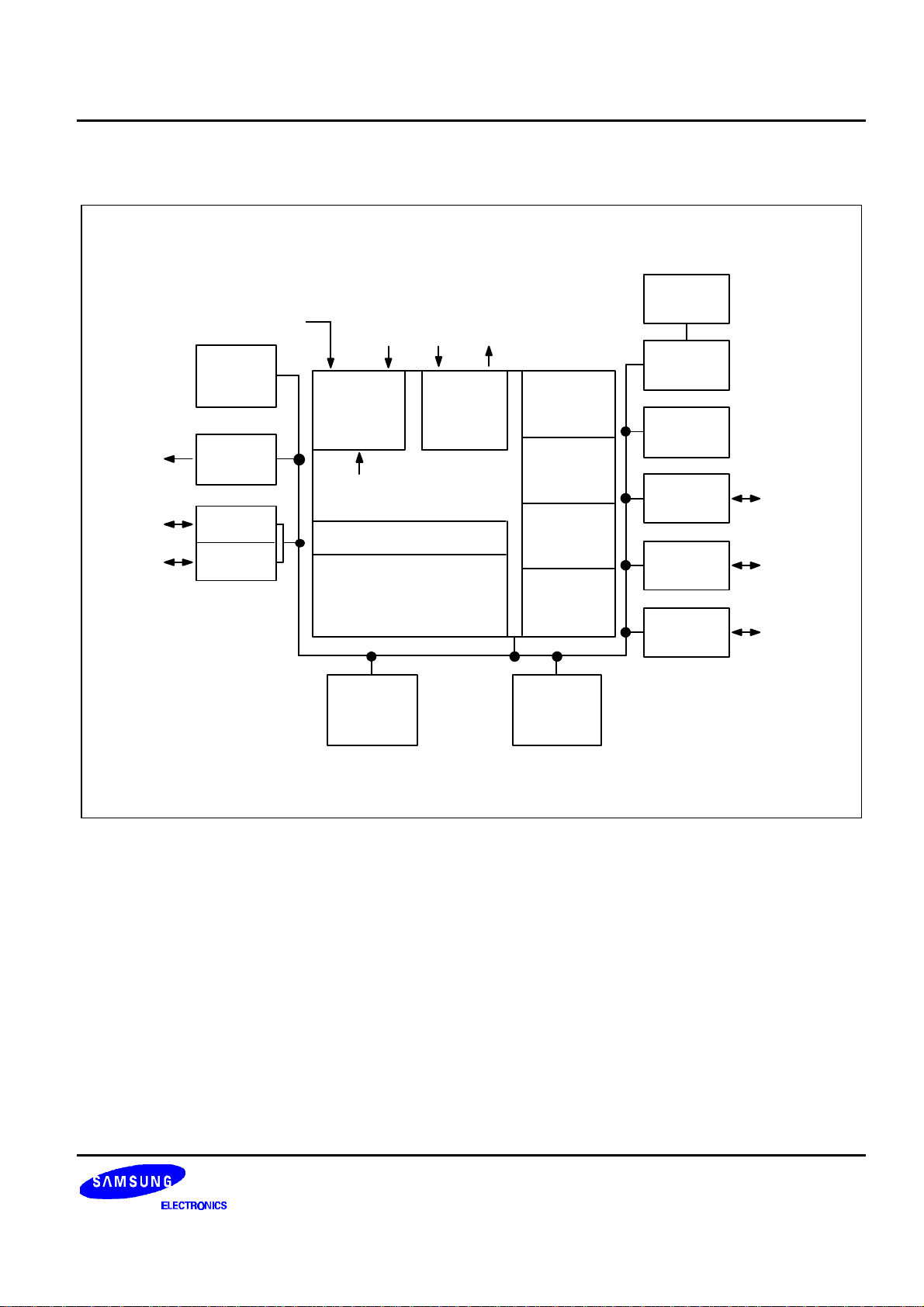
The S3C7544 single-chip CMOS microcontroller is designed for high-performance using Samsung's newest
4-bit CPU core, SAM47 (Samsung Arrangeable Microcontrollers).
With a versatile 8-bit timer/counter and a D/A converter, the S3C7544 offers an excellent design solution for a
wide variety of telecommunication applications.
Up to 17 pins of the 24-pin SDIP package can be dedicated to I/O. Four vectored interrupts provide fast response
to internal and external events. In addition, the S3C7544’s advanced CMOS technology has realized substantially
lower power consumption with a wide operating voltage range — all at a substantially lower cost.
OTP
The S3C7544 microcontroller is also available in OTP (One Time Programmable) version, S3P7544.
S3P7544 microcontroller has an on-chip 4-Kbyte one-time-programmable EPROM instead of masked ROM. The
S3P7544 is comparable to S3C7544, both in function and in pin configuration.
1-1
Page 2

PRODUCT OVERVIEW S3C7544/P7544
FEATURES SUMMARY
Memory
• 512 × 4-bit RAM
• 4096 × 8-bit ROM
I/O Pins
• 17 pins I/O
• N-channel open-drain I/O: 8 pins
8-Bit Basic Timer
• Programmable interval timer
• Watchdog timer
Interval 8-Bit Timer/Counter
• Programmable interval timer
• External event counter function
• Timer/counter clock output to TCLO0 pin
Buzzer Output
• Four frequency output to BUZ pin
Bit Sequential Carrier
• Supports 16-bit serial data transfer in arbitrary
format
Power-Down Modes
• Idle mode (only CPU clock stops)
• Stop mode (system clock stops)
Oscillation Sources
• Crystal, or ceramic for system clock
• Crystal, ceramic: 0.4–6.0 MHz
• CPU clock divider circuit (by 4, 8, or 64)
Instruction Execution Times
• 0.95, 1.91, and 15.3 µs at 4.19 MHz
• 0.67, 1.33, 10.7 µs at 6.0 MHz
Operating Temperature
• – 40 °C to 85 °C
D/A Converter
• 8-bit D/A converter
Interrupts
• Two external interrupt vectors
• Two internal interrupt vectors
• One quasi-interrupt
Memory-Mapped I/O Structure
• Data memory bank 15
Operating Voltage Range
• 1.8 V to 5.5 V (at 3 MHz)
• 2.7 V to 5.5 V (at 6 MHz)
Package Types
• 24-pin SOP-375
• 24-pin SDIP-300
1-2
Page 3
S3C7544/P7544 PRODUCT OVERVIEW
BLOCK DIAGRAM
Watchdog
Timer
DAO
P4.0–P4.3
P5.0–P5.3
INT0, INT1
8-bit
Timer/
Counter
D/A
Converter
I/O Port 4
I/O Port 5
RESET
Interrupt
Control
Block
Internal
Interrupts
Instruction Decoder
Arithmetic Logic Unit
X
IN
Clock
X
OUT
Stack
Pointer
Program
Counter
Program
Status
Word
Flags
Basic
Timer
Buzzer
I/O Port 0
I/O Port 1
P0.0/INT0
P0.1/INT1
P0.2/KS0
P0.3/KS1
P1.0/TCL0
P1.1/TCLO0
P1.2/CLO
P1.3/BUZ
512 x 4-bit
Data
Memory
4 K byte
Program
Memory
Figure 1-1. S3C7544 Simplified Block Diagram
I/O Port 2
P2.0
1-3
Page 4
PRODUCT OVERVIEW S3C7544/P7544
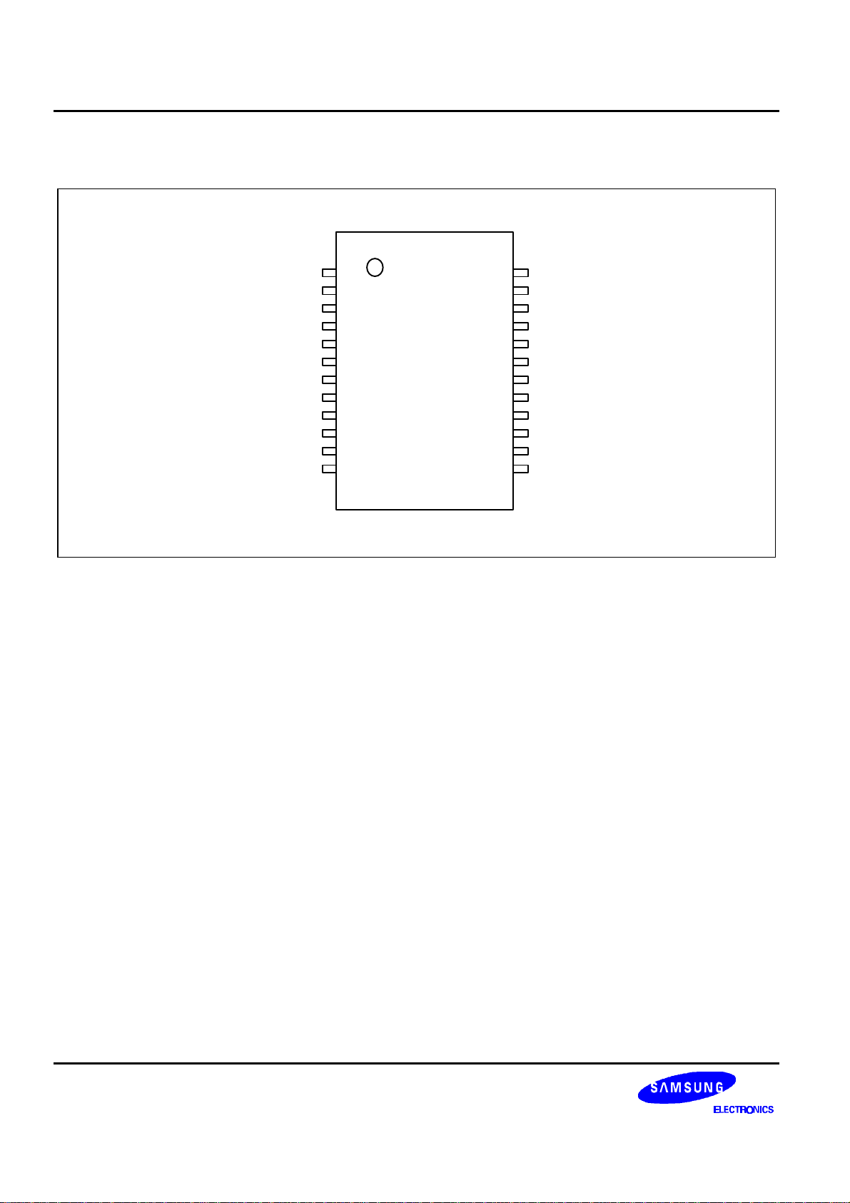
PIN ASSIGNMENTS
VSS
X
OUT
XIN
TEST
P0.0/INT0
DAO
P0.1/INT1
RESET
P0.2/KS0
P0.3/KS1
P1.0/TCL0
P1.1/TCLO0
1
2
3
4
5
6
7
8
9
10
11
12
24 SDIP-300
24 SOP-375
24
23
22
S3C7544
21
20
19
18
17
16
15
14
13
Figure 1-2. S3C7544 Pin Assignment Diagrams
VDD
P5.3
P5.2
P5.1
P5.0
P4.3
P4.2
P4.1
P4.0
P2.0
P1.3/BUZ
P1.2/CLO
1-4
Page 5
S3C7544/P7544 PRODUCT OVERVIEW
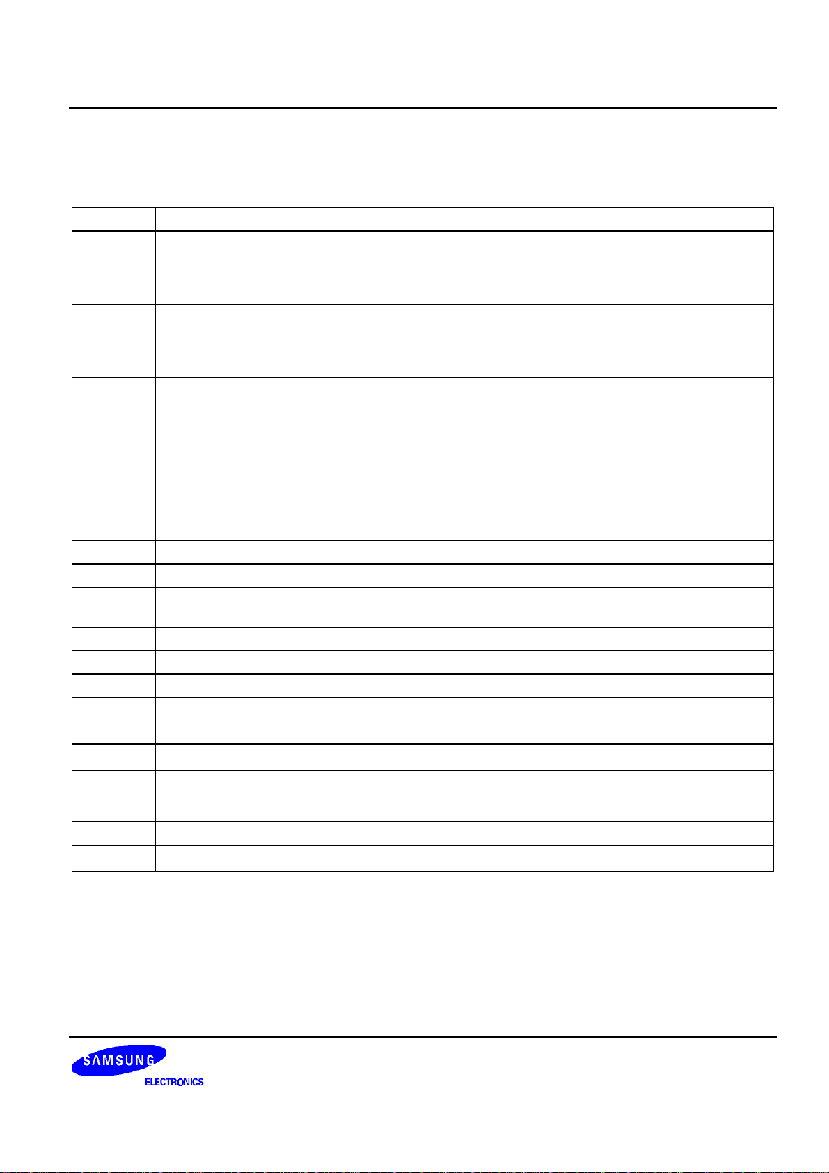
PIN DESCRIPTIONS
Table 1-1. S3C7544 Pin Descriptions
Pin Name Pin Type Description Share Pin
P0.0
P0.1
P0.2
P0.3
P1.0
P1.1
P1.2
P1.3
P2.0 I/O 1-bit I/O port. 1- or 4-bit read/write and test is possible.
I 4-bit I/O port. 1- or 4-bit read/write and test is possible.
Pull-up resistors are assignable to input pins by software and are
automatically disabled for output pins. Pins are individually
configurable as input or output.
I/O 4-bit I/O port. 1- or 4-bit read/write and test is possible.
Pull-up resistors are assignable to input pins by software and are
automatically disabled for output pins. Pins are individually
configurable as input or output.
INT0
INT1
KS0
KS1
TCL0
TCLO0
CLO
BUZ
–
Pull-up resistors are assignable to input pins by software and are
automatically disabled for output pins.
P4.0–P4.3
I/O 4-bit I/O port. 1- or 4-bit read/write and test is possible.
–
Pins are individually configurable as input or output.
P5.0–P5.3
Pull-up resistors are assignable to input pins by software and are
automatically disabled for output pins.
The N-channel open drain or push-pull output can be selected by
software (1-bit unit).
INT0 I/O External interrupts with rising/falling edge detection P0.0
INT1 I/O External interrupts with rising/falling edge detection P0.1
KS0
KS1
I/O Quasi-interrupt input with falling edge detection P0.2
P0.3
TCL0 I/O External clock input for timer/counter P1.0
TCLO0 I/O Timer/counter clock output P1.1
CLO I/O CPU clock output P1.2
BUZ I/O 0.5, 1, 2, or 4 kHz frequency output at 4.19 MHz for buzzer sound P1.3
DAO O 8-bit D/A converter output –
V
DD
V
SS
RESET
– Main power supply –
– Ground –
I Reset signal –
TEST I Chip test input pin. Hold GND when the device is operating. –
XIN, X
OUT
– Crystal, ceramic oscillator signal for system clock –
1-5
Page 6

PRODUCT OVERVIEW S3C7544/P7544
Table 1-2. Overview of S3C7544 Pin Data
SDIP Pin Numbers Share Pins I/O Type Reset Value Circuit Type
V
X
SS
OUT
, X
IN
– – – –
– – – –
TEST – I – –
P0.0, P0.1 INT0, INT1 I/O Input D-4
RESET
P0.2
P0.3
P1.0
P1.1
P1.2
P1.3
– I – B
KS0
I/O Input D-4
KS1
TCL0
I/O Input D-2
TCLO0
CLO
BUZ
P2.0 – I/O Input D-2
DAO – O Output –
P4.0–P4.3 – I/O Input E-2
P5.0–P5.3 – I/O Input E-2
V
DD
– – – –
1-6
Page 7

S3C7544/P7544 PRODUCT OVERVIEW
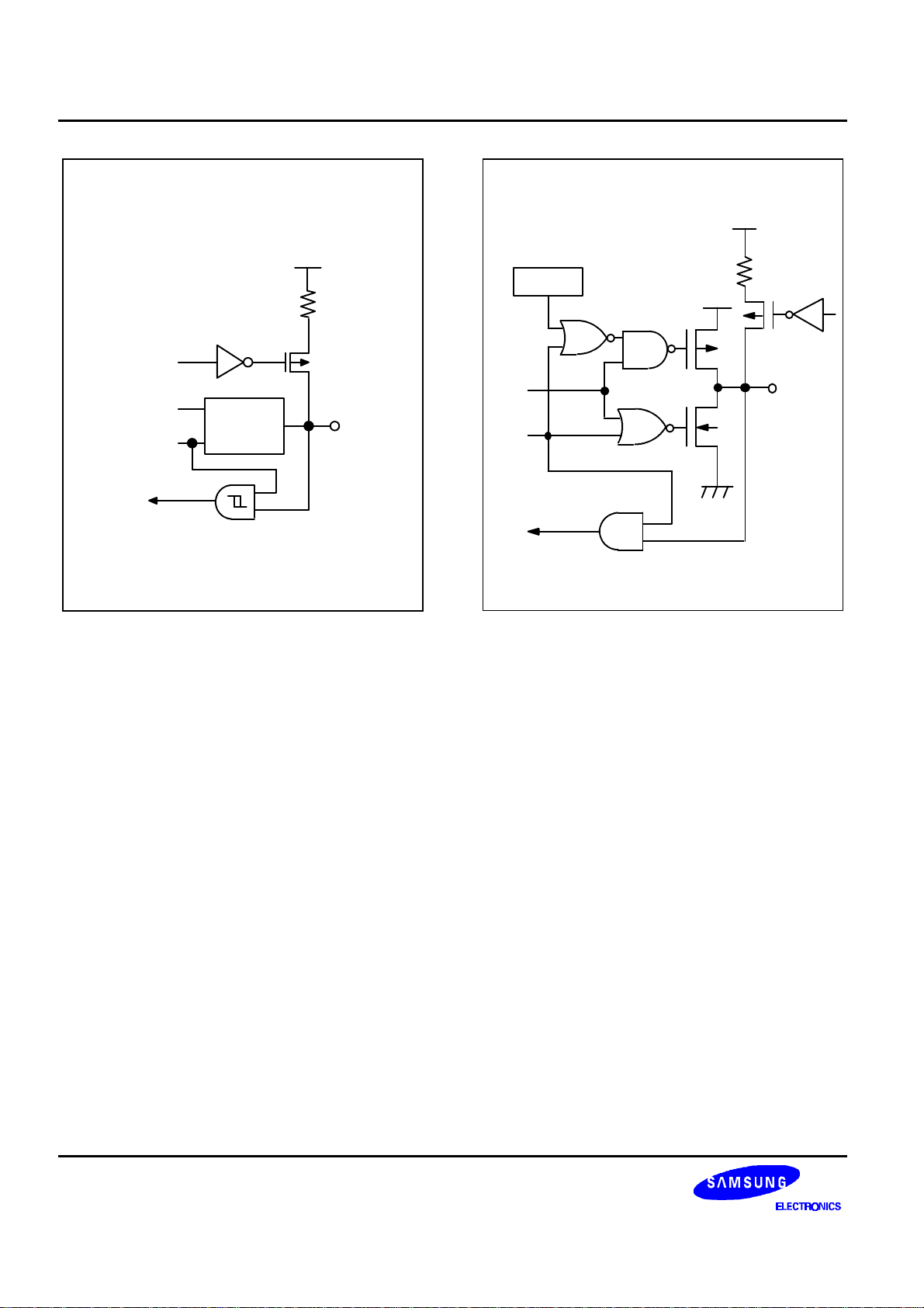
PIN CIRCUIT DIAGRAMS
V
DD
P-Channel
IN
N-Channel
Figure 1-3. Pin Circuit Type A
V
DD
Data
Output
Disable
V
DD
P-Channel
N-Channel
Figure 1-5. Pin Circuit Type C
V
DD
Out
Pull-up
Resistor
IN
Schmitt Trigger
Figure 1-4. Pin Circuit Type B
Pull-up
Enable
Data
Output
Disable
Circuit
Type C
P-Channel
Figure 1-6. Pin Circuit Type D-2
In/Out
1-7
Page 8
PRODUCT OVERVIEW S3C7544/P7544
V
DD
V
DD
PNE
V
DD
Pull-Up
Resistor
Pull-up
Enable
Data
Output
Circuit
Type C
P-Channel
Disable
Figure 1-7. Pin Circuit Type D-4
Resistor
Enable
In/Out
Data
In/Out
Output
Disable
Figure 1-8. Pin Circuit Type E-2
1-8
Page 9

S3C7544/P7544 ELECTRICAL DATA
14 ELECTRICAL DATA
OVERVIEW
In this section, S3C7544 electrical characteristics are presented in tables and graphs. The information is
arranged in the following order:
Standard Electrical Characteristics
— Absolute maximum ratings
— D.C. electrical characteristics
— Main system clock oscillator characteristics
— Subsystem clock oscillator characteristics
— I/O capacitance
— A.C. electrical characteristics
— Operating voltage range
Miscellaneous Timing Waveforms
— A.C timing measurement point
— Clock timing measurement at X
— Clock timing measurement at XT
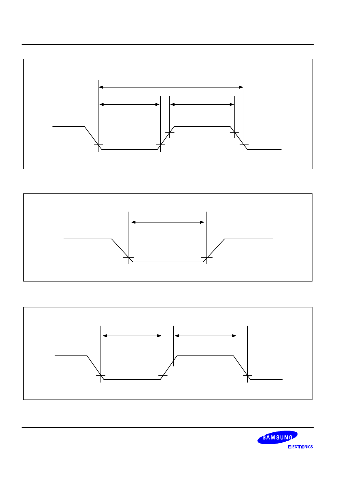
— TCL timing
— Input timing for RESET
— Input timing for external interrupts
— Serial data transfer timing
Stop Mode Characteristics and Timing Waveforms
— RAM data retention supply voltage in stop mode
— Stop mode release timing when initiated by RESET
— Stop mode release timing when initiated by an interrupt request
in
in
14-1
Page 10
ELECTRICAL DATA S3C7544/P7544
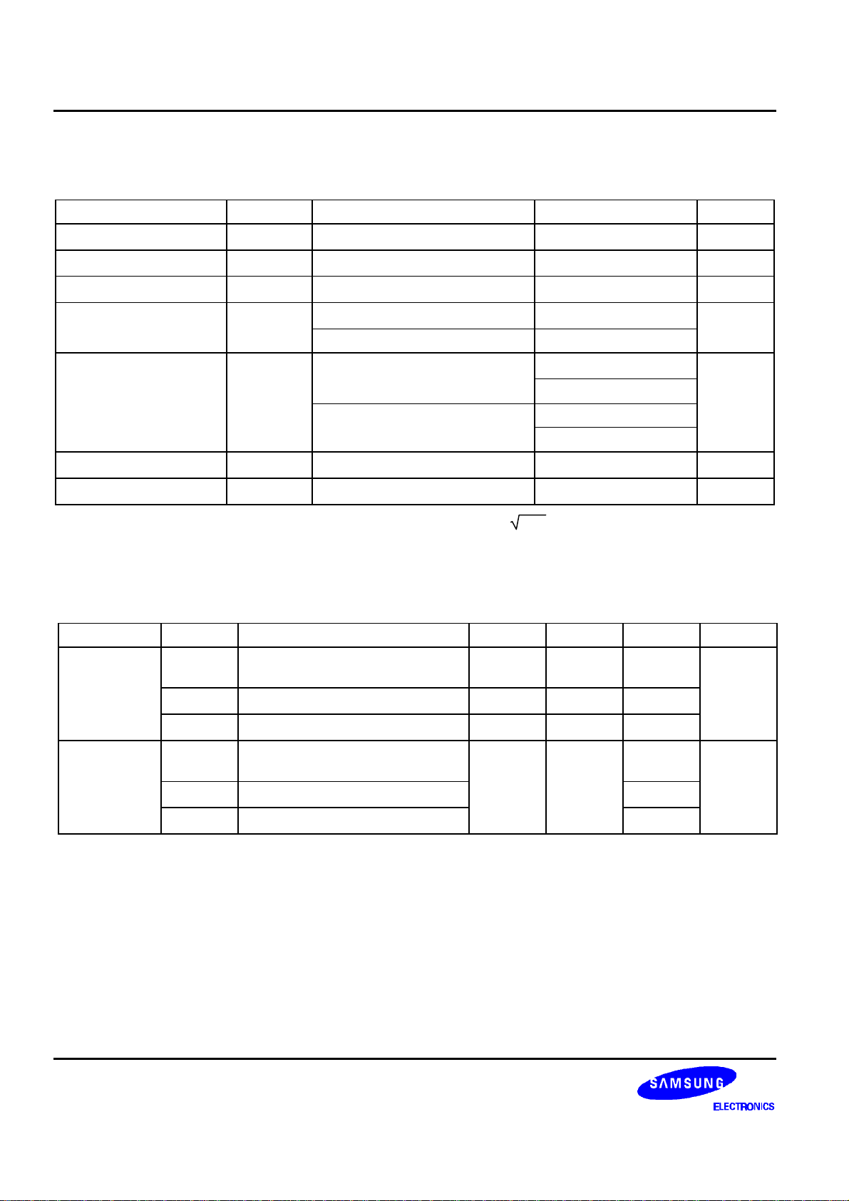
Table 14-1. Absolute Maximum Ratings
(TA = 25 °C)
Parameter Symbol Conditions Rating Units
Supply Voltage
Input Voltage
Output Voltage
Output Current High
V
DD
V
I
V
O
I
OH
All I/O ports
One I/O port active – 5 mA
– – 0.3 to + 6.5 V
– 0.3 to V
–
– 0.3 to VDD + 0.3
DD
+ 0.3
V
V
All I/O ports active – 35
Output Current Low
I
OL
One I/O port active + 30 (peak) mA
(note)
+ 15
All I/O ports active + 100 (peak)
(note)
+ 60
Operating Temperature
Storage Temperature
T
A
T
stg
– – 40 to + 85
– – 65 to + 150
°
C
°
C
NOTE: The values for output current low (IOL) are calculated as peak value × Duty .
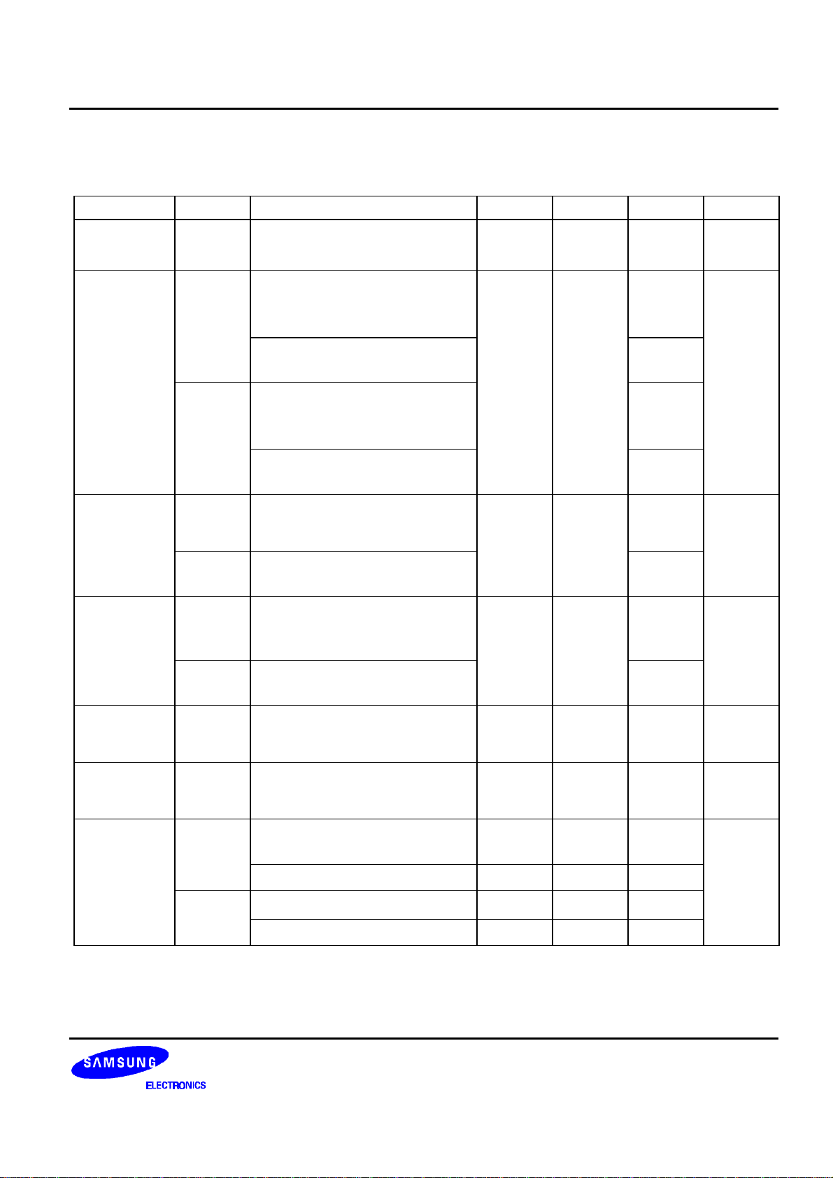
Table 14-2. D.C. Electrical Characteristics
(TA = – 40 °C to + 85 °C, VDD = 1.8 V to 5.5 V)
Parameter Symbol Conditions Min Typ Max Units
Input High
V
IH1
All input pins except V
IH2–VIH3
0.7 V
DD
–
V
DD
Voltage
Input Low
V
IH2
V
IH3
V
IL1
P0 and RESET
XIN and X
OUT
All input pins except V
IH2–VIH3
0.8 V
DD
V
– 0.1
DD
– –
–
–
V
DD
V
DD
0.3 V
DD
Voltage
V
IL2
V
IL3
P0 and RESET
XIN and X
OUT
0.2 V
0.1
DD
V
V
14-2
Page 11
S3C7544/P7544 ELECTRICAL DATA
Table 14-2. D.C. Electrical Characteristics (Continued)
(T
= – 40 °C to + 85 °C, VDD = 1.8 V to 5.5 V)
A
Parameter Symbol Conditions Min Typ Max Units
Output High
Voltage
V
OH
V
= 4.5 V to 5.5 V
DD
IOH = – 1 mA
V
DD
– 1.0
– – V
Output Low
Voltage
Input High
Leakage
Current
Input Low
Leakage
Current
Output High
Leakage
Current
Output Low
Leakage
Current
Pull-up
Resistor
V
V
I
LIH1
I
LIH2
I
LIL1
I
LIL2
I
LOH
I
R
R
OL1
OL2
LOL
L1
L2
V
= 4.5 V to 5.5 V
DD
IOL = 15 mA
Ports 4, 5
V
= 1.8 V to 5.5 V
DD
IOL = 1.6 mA
VDD = 4.5V to 5.5 V
I
= 4 mA
OL
All out ports except ports 4, 5
V
= 1.8 V to 5.5 V
DD
IOL = 1.6 mA
VIN = V
DD
All input pins except XIN and X
VIN = V
XIN and X
V
All input pins except XIN, X
IN
DD
OUT
= 0 V
OUT
and RESET
V
= 0 V
IN
XIN and X
VO = V
OUT
DD
All output pins
V
= 0 V
O
All output pins
V
= 5 V; V
DD
except
V
= 3 V
DD
V
= 5 V; V
DD
V
= 3 V
DD
= 0 V
I
RESET
= 0 V; RESET
I
OUT
– – 2 V
0.4
2
0.6
– – 3
20
– – – 3
– 20
– – 3
– – – 3
25 45 100
50 90 200
100 220 400
200 450 800
µA
µA
µA
µA
kΩ
14-3
Page 12
ELECTRICAL DATA S3C7544/P7544
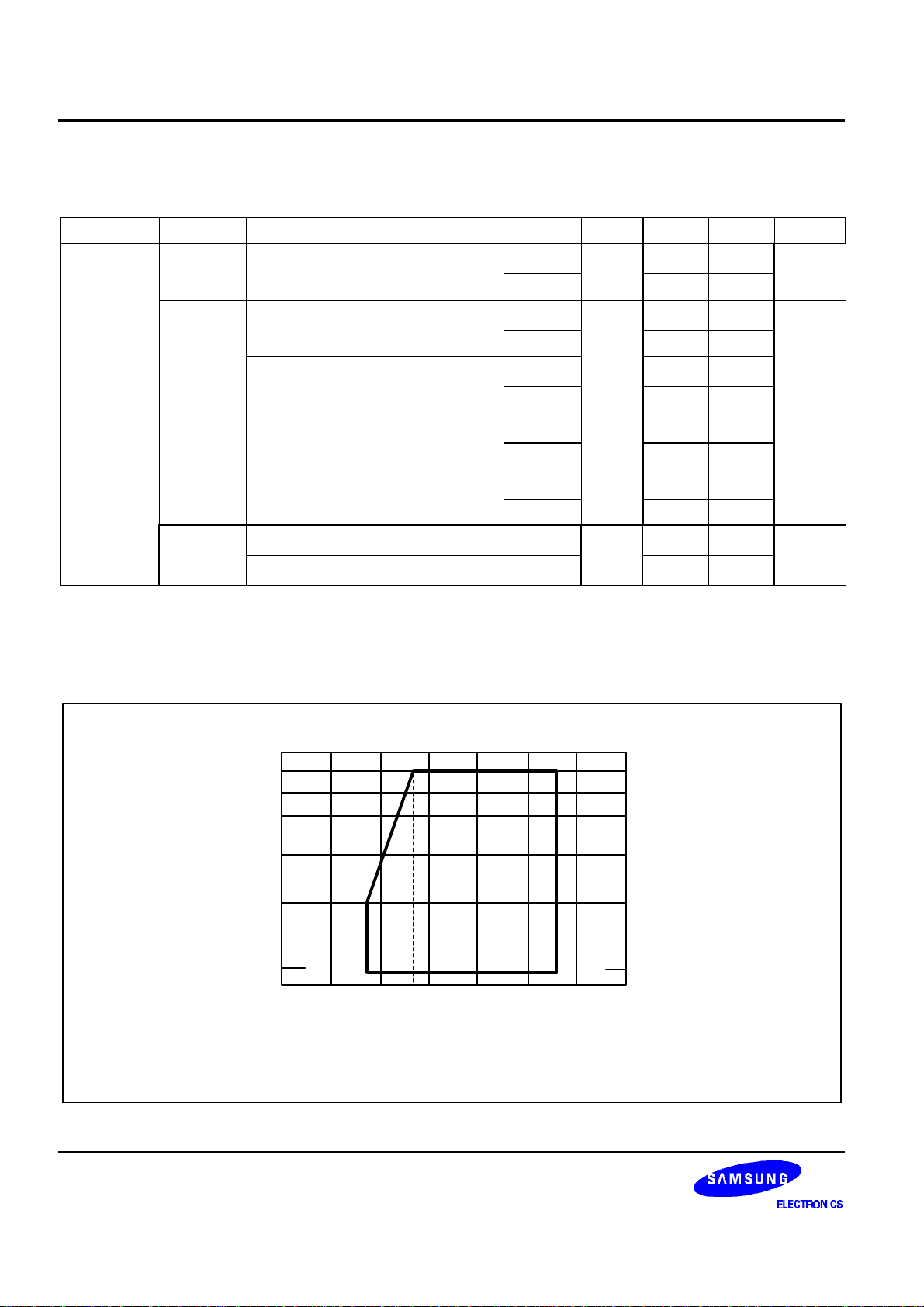
Table 14-2. D.C. Electrical Characteristics (Concluded)
(T
= – 40 °C to + 85 °C, VDD = 1.8 V to 5.5 V)
A
Parameter Symbol Conditions Min Typ Max Units
Supply
Current
(1)
I
DD1
Run mode; V
= 5.0 V ± 10%
DD
6.0MHz – 3.4 10.0
(DAC on) Crystal oscillator; C1 = C2 = 22pF 4.19MHz 2.7 8.0
I
DD2
Run mode; V
= 5.0 V ± 10%
DD
6.0MHz – 2.3 8.0
mA
mA
(DAC off) Crystal oscillator; C1 = C2 = 22pF 4.19MHz 1.7 5.5
V
= 3 V ± 10%
DD
6.0MHz 1.1 4.0
4.19MHz 0.8 3.0
I
DD3
Idle mode; V
= 5.0 V ± 10%
DD
6.0MHz – 0.7 2.5
mA
Crystal oscillator; C1 = C2 = 22pF 4.19MHz 0.5 1.8
V
= 3 V ± 10%
DD
6.0MHz 0.3 1.5
4.19MHz 0.2 1.0
I
DD4
Stop mode; V
Stop mode; V
= 5.0 V ± 10%
DD
= 3.0 V ± 10%
DD
– 0.2 3.0
0.1 2.0
µA
NOTES:
1. D.C. electrical values for supply current (I
resistors.
2. I
typical values are measured when DADATA register value is 055H.
DD1
CPU CLOCK
1.5 MHz
0.75 MHz
15.625 kHz
1 2
CPU CLOCK = 1/n x oscillator frequency (n = 4, 8 or 64)
DD1
1.8
to I
) do not include the current drawn through internal pull-up
DD3
2.7
3 4 5 6 7
SUPPLY VOLTAGE (V)
Main Osc. Freq.
6 MHz
3 MHz
400 kHz
14-4
Figure 14-1. Standard Operating Voltage Range
Page 13
S3C7544/P7544 ELECTRICAL DATA
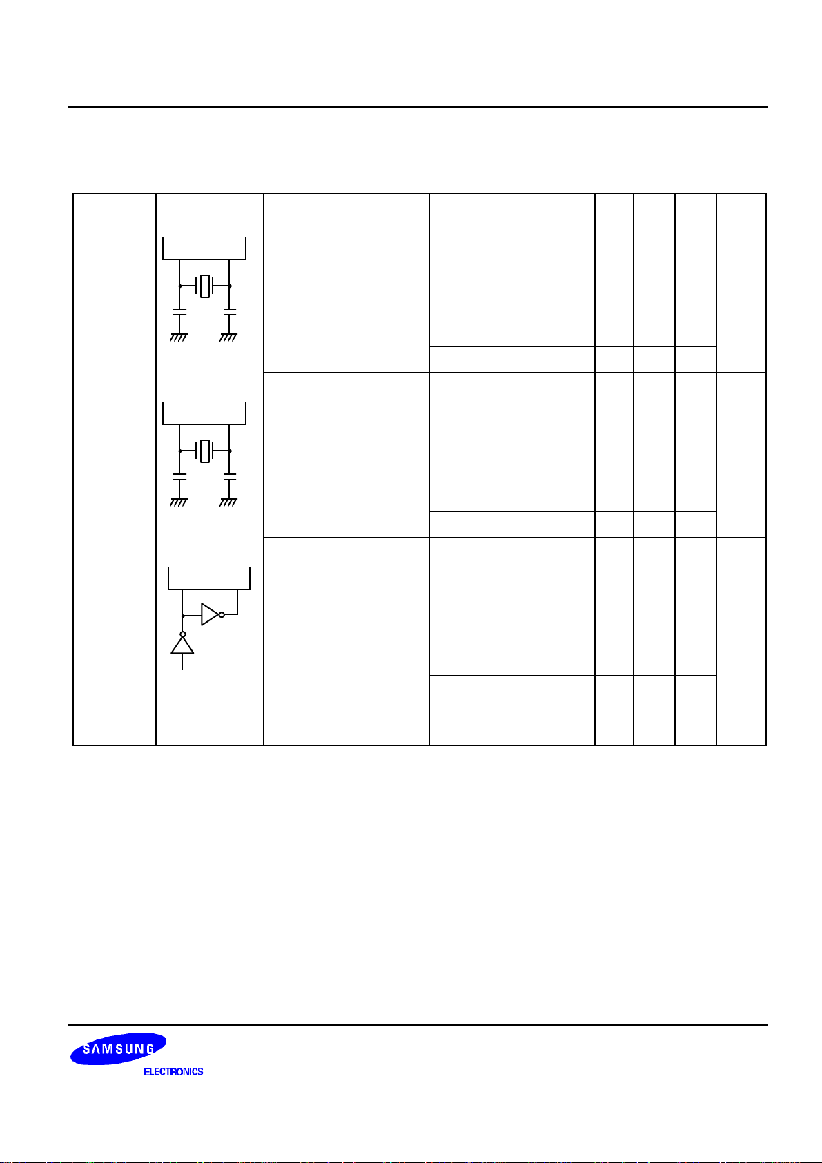
Table 14-3. Oscillators Characteristics
(T
= – 40 °C + 85 °C, VDD = 1.8 V to 5.5 V)
A
Oscillator Clock
Configuration
Ceramic
Xin Xout
Oscillator
C1 C2
Crystal
Xin Xout
Oscillator
C1 C2
External
Xin Xout
Clock
Parameter Test Condition Min Typ Max Units
Oscillation frequency
Stabilization time
(2)
Oscillation frequency
Stabilization time
XIN input frequency
(2)
(1)
(1)
VDD = 2.7 V to 5.5 V
VDD = 1.8 V to 5.5 V
VDD = 3.0 V
(1)
VDD = 2.7 V to 5.5 V
VDD = 1.8 V to 5.5 V
VDD = 3.0 V
VDD = 2.7 V to 5.5 V
0.4 – 6.0 MHz
0.4 – 3
– – 4 ms
0.4 – 6.0 MHz
0.4 – 3
– – 10 ms
0.4 – 6.0 MHz
XIN input high and low
VDD = 1.8 V to 5.5 V
– 83.3 – 1250 ns
0.4 – 3
level width (tXH, tXL)
NOTES:
1. Oscillation frequency and XIN input frequency data are for oscillator characteristics only.
2. Stabilization time is the interval required for oscillating stabilization after a power-on occurs, or when stop mode is
terminated.
14-5
Page 14
ELECTRICAL DATA S3C7544/P7544
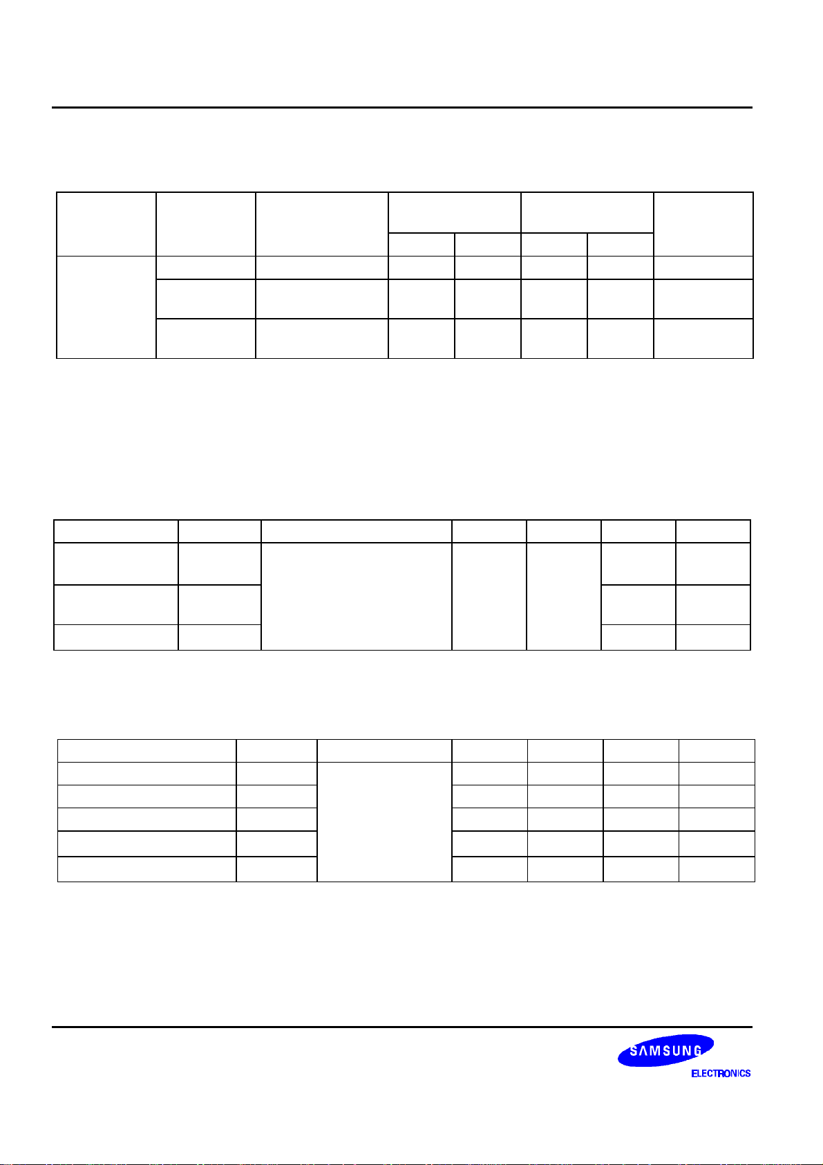
Table 14-4. Recommended Oscillator Constants
(TA = – 40 °C + 85 °C, VDD = 1.8 V to 5.5 V)
Manufacturer Series
Number
Frequency Range Load Cap (pF) Oscillator Voltage
(1)
Range (V)
C1 C2 MIN MAX
TDK
FCRM5
FCRMC5
3.58 MHz–6.0 MHz 33 33 2.0 5.5 Leaded Type
3.58 MHz–6.0 MHz
(2) (2)
2.0 5.5 On-chip C
Leaded Type
CCRMC3
3.58 MHz–6.0 MHz
(3) (3)
2.0 5.5 On-chip C
SMD Type
NOTES:
1. Please specify normal oscillator frequency.
2. On-chip C: 30pF built in.
3. On-chip C: 38pF built in.
Table 14-5. Input/Output Capacitance
(TA = 25 °C, V
DD
= 0 V )
Parameter Symbol Condition Min Typ Max Units
C
C
OUT
IN
f = 1 MHz; Unmeasured pins
are returned to V
SS
– – 15 pF
15 pF
Input
Capacitance
Output
Capacitance
I/O Capacitance
C
IO
15 pF
Remarks
Table 14-6. D/A Converter Electrical Characteristics
(T
= – 40 °C to + 85 °C, VDD = 3.5 V to 5.5 V, VSS = 0 V)
A
Parameter Symbol Condition Min Typ Max Units
Resolution – – – – 8 bits
Absolute Accuracy – – 3 – 3 LSB
Differential Linearity Error DLE – 1 – 1 LSB
Setup Time
Output Resistance
14-6
t
su
R
O
– – 5
4.5 5 5.5
µs
KΩ
Page 15
S3C7544/P7544 ELECTRICAL DATA
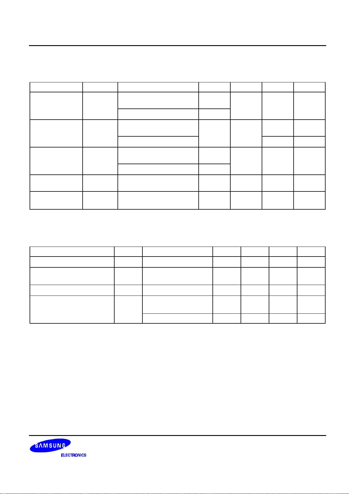
Table 14-7. A.C. Electrical Characteristics
(TA = – 40 °C to + 85 °C, V
= 1.8 V to 5.5 V)
DD
Parameter Symbol Conditions Min Typ Max Units
Instruction Cycle
t
CY
V
= 2.7 V to 5.5 V
DD
0.67 – 64
Time
TCL0 Input
VDD = 1.8 V to 5.5 V
f
TI
V
= 2.7 V to 5.5 V
DD
1.33
0 – 1.5 MHz
Frequency
TCL0 Input High,
t
TIH,
VDD = 1.8 V to 5.5 V
t
TIL
V
= 2.7 V to 5.5 V
DD
0.48 – –
1 MHz
Low Width
Interrupt Input
t
INTH, tINTL
VDD = 1.8 V to 5.5 V
INT0, INT1, KS0–KS1 10 – –
1.8
High, Low Width
RESET Input Low
t
RSL
Input – – 10
Width
Table 14-8. RAM Data Retention Supply Voltage in Stop Mode
(TA = – 40 °C to + 85 °C)
µs
µs
µs
µs
Parameter Symbol Conditions Min Typ Max Unit
Data retention supply voltage
Data retention supply current
Release signal set time
Oscillator stabilization wait
(1)
time
NOTES:
1. During oscillator stabilization wait time, all CPU operations must be stopped to avoid instability during oscillator
start-up.
2. Use the basic timer mode register (BMOD) interval timer to delay the execution of CPU instructions during the wait time.
V
DDDR
I
DDDR
t
SREL
t
WAIT
– 1.8 – 5.5 V
V
DDDR
= 1.8 V
– 0 – –
Released by RESET
Released by interrupt –
– 0.1 10
–
217/fx
(2)
– ms
– ms
µA
µs
14-7
Page 16
ELECTRICAL DATA S3C7544/P7544
TIMING WAVEFORMS
INTERNAL RESET
OPERATION
V
DD
RESET
V
DD
~
~
~
~
EXECUTION OF
STOP INSTRUCTION
STOP MODE
DATA RETENTION MODE
V
DDDR
t
SREL
IDLE MODE
t
WAIT
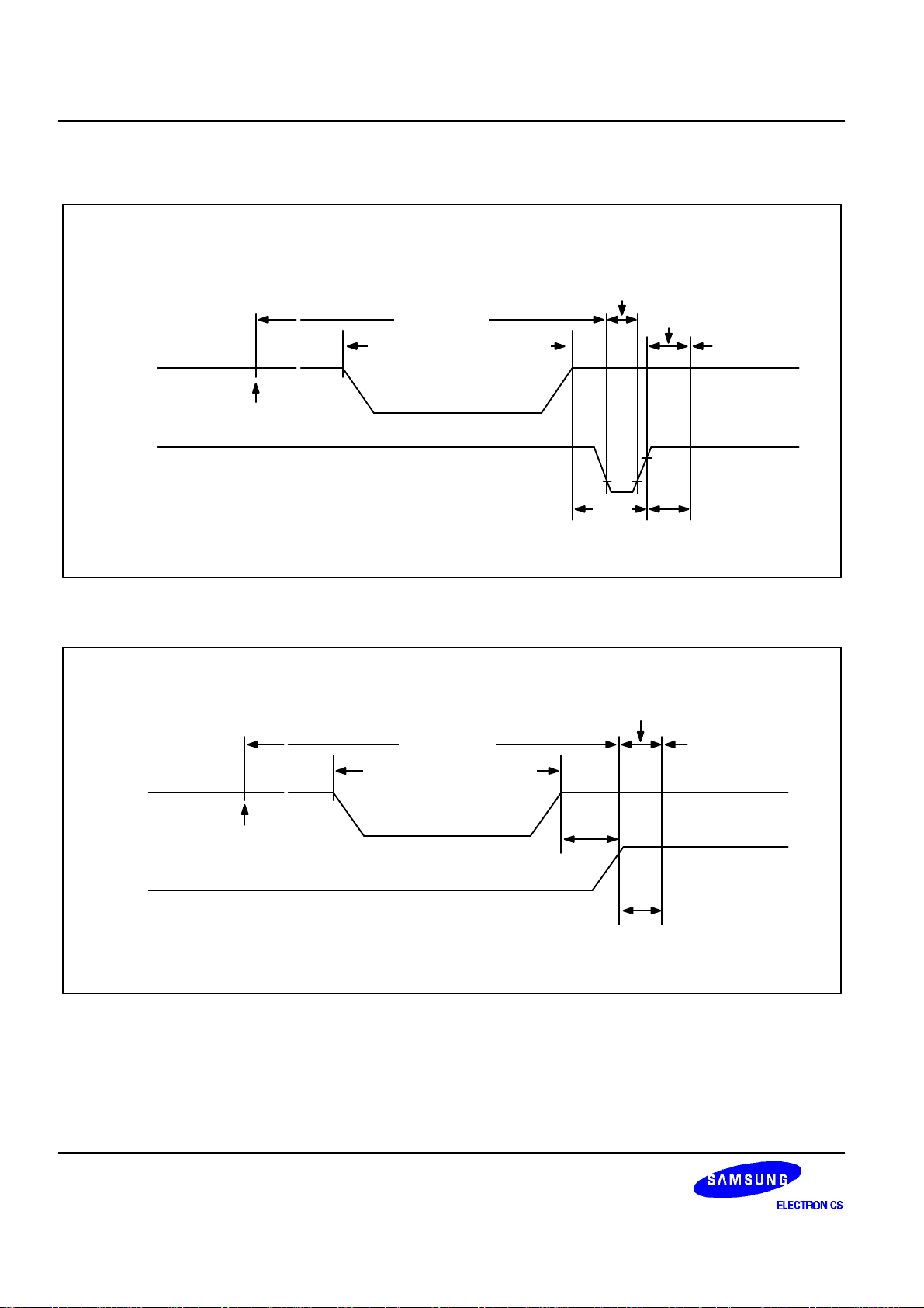
Figure 14-2. Stop Mode Release Timing When Initiated by RESETRESET
IDLE MODE
~
~
~
~
STOP MODE
DATA RETENTION
OPERATING
MODE
NORMAL
OPERATING
MODE
14-8
EXECUTION OF
STOP INSTRUCTION
POWER-DOWN MODE TERMINATING
(INTERRUPT REQUEST)
V
DDDR
t
SREL
t
WAIT
Figure 14-3. Stop Mode Release Timing When Initiated by Interrupt Request
Page 17
S3C7544/P7544 ELECTRICAL DATA
0.8 V
0.2 V
DD
DD
MEASUREMENT
POINTS
0.8 V
0.2 V
DD
DD
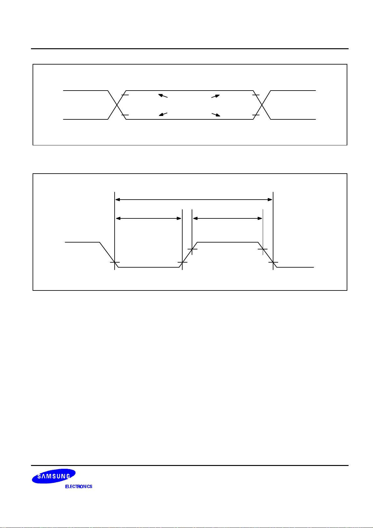
Figure 14-4. A.C. Timing Measurement Points (Except for XIN)
1 / f
x
t
XL
X
IN
t
XH
V
DD
0.1 V
– 0.1 V
Figure 14-5. Clock Timing Measurement at X
IN
14-9
Page 18
ELECTRICAL DATA S3C7544/P7544
1 / f
TI
TCL
RESET
t
TIL
Figure 14-6. TCL Timing
t
RSL
t
TIH
0.2 V
DD
0.7 V
0.3 V
DD
DD
14-10
INT0, 1
KS0 to KS1
Figure 14-7. Input Timing for RESETRESET Signal
t
INTL
0.8 V
0.2 V
DD
DD
t
INTH
Figure 14-8. Input Timing for External Interrupts
Page 19
S3C7544/P7544 MECHANICAL DATA
°
15 MECHANICAL DATA
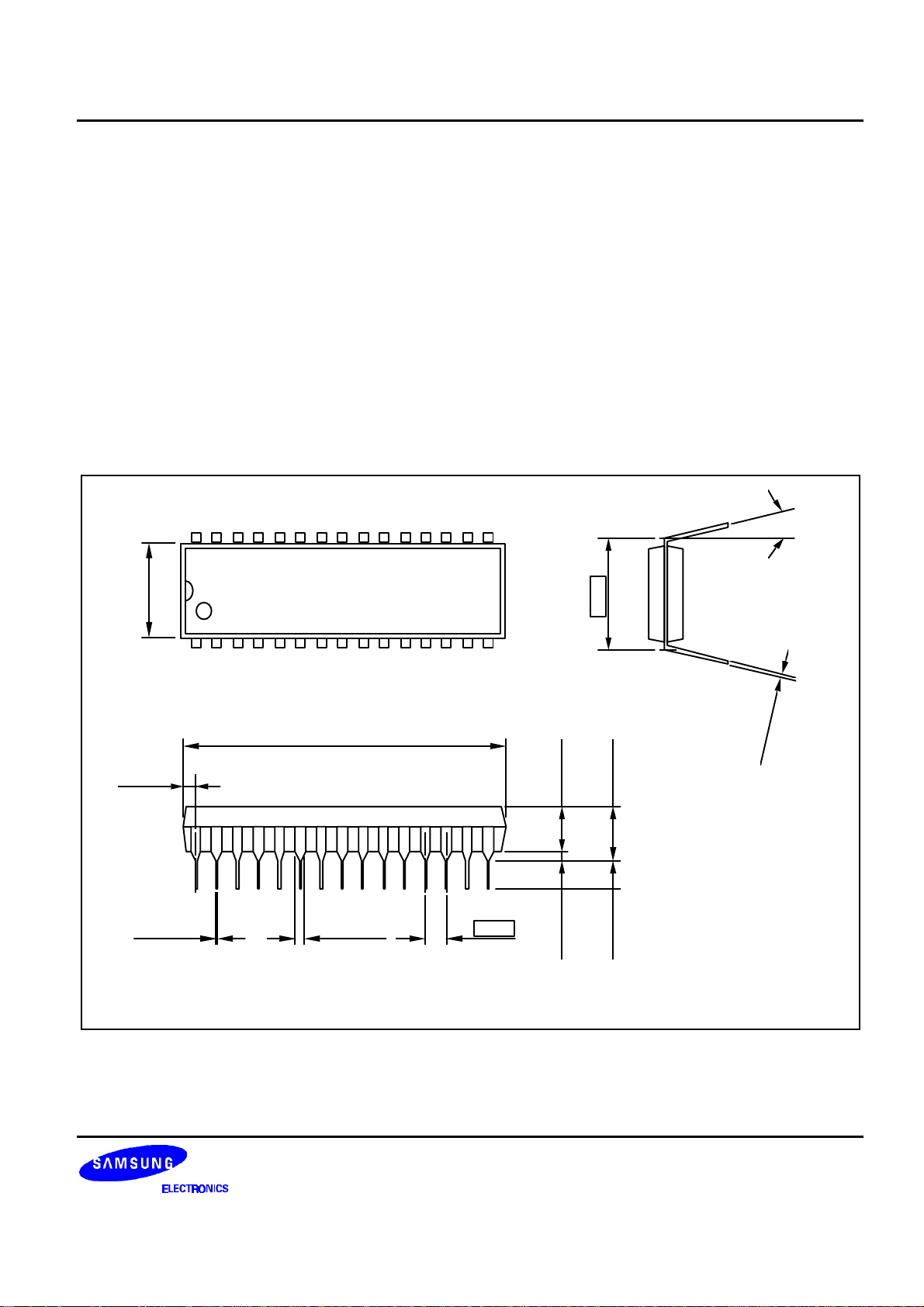
This section contains the following information about the device package:
— Package dimensions in millimeters
— Pad diagram
— Pad/pin coordinate data table
8.94 ± 0.2
(1.30)
0.56 ± 0.1
30 16
30-SDIP-400
#1 15
27.48 ± 0.2
1.12 ± 0.1
1.778
10.16
3.81 ± 0.2
0.51MIN
3.30 ± 0.3 5.08MAX
+0.1
– 0.05
0.25
0 ~ 15
NOTE
: Typical dimensions are in millimeters.
Figure 15-1. 30-SDIP-400 Package Dimensions
15–1
Page 20
S3C7544/P7544 S3P7544 OTP
16 S3P7544 OTP
OVERVIEW
The S3P7544 single-chip CMOS microcontroller is the OTP (One Time Programmable) version of the S3C7544
microcontroller. It has an on-chip OTP ROM instead of masked ROM. The EPROM is accessed by serial data
format.
The S3P7544 is fully compatible with the S3C7544, both in function and in pin configuration. Because of its
simple programming requirements, the S3P7544 is ideal for use as an evaluation chip for the S3C7544.
VSS/VSS
X
OUT
XIN
VPP/TEST
P0.0/INT0
DAO
P0.1/INT1
RESETRESET /RESET
P0.2/KS0
P0.3/KS1
P1.0/TCL0
P1.1/TCLO0
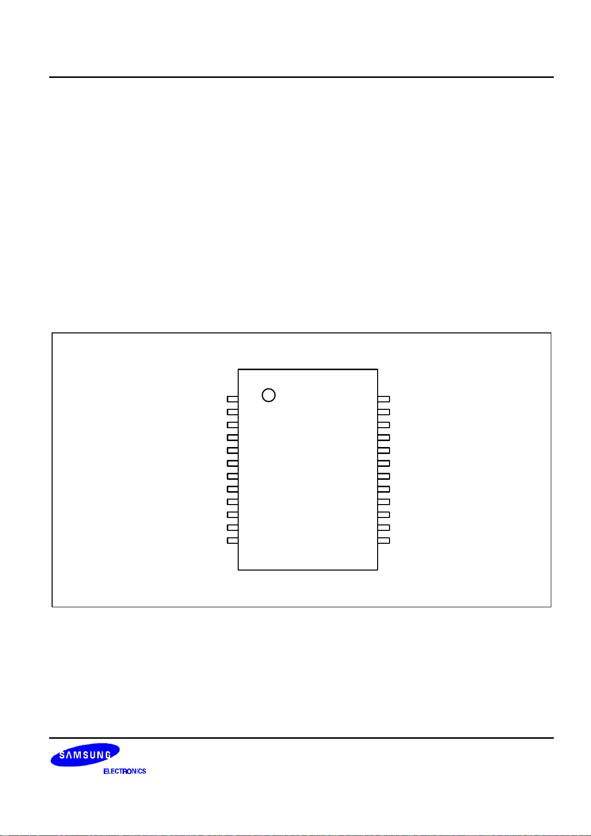
Figure 16-1. S3P7544 Pin Assignments (24 SOP-375, 24 SDIP-300 Package)
1
2
3
4
5
6
7
8
9
10
11
12
24 SDIP-300
24 SOP-375
S3P7544
24
23
22
21
20
19
18
17
16
15
14
13
VDD/VDD
P5.3/SCLK
P5.2/SDAT
P5.1
P5.0
P4.3
P4.2
P4.1
P4.0
P2.0
P1.3/BUZ
P1.2/CLO
16-1
Page 21
S3P7544 OTP S3C7544/P7544
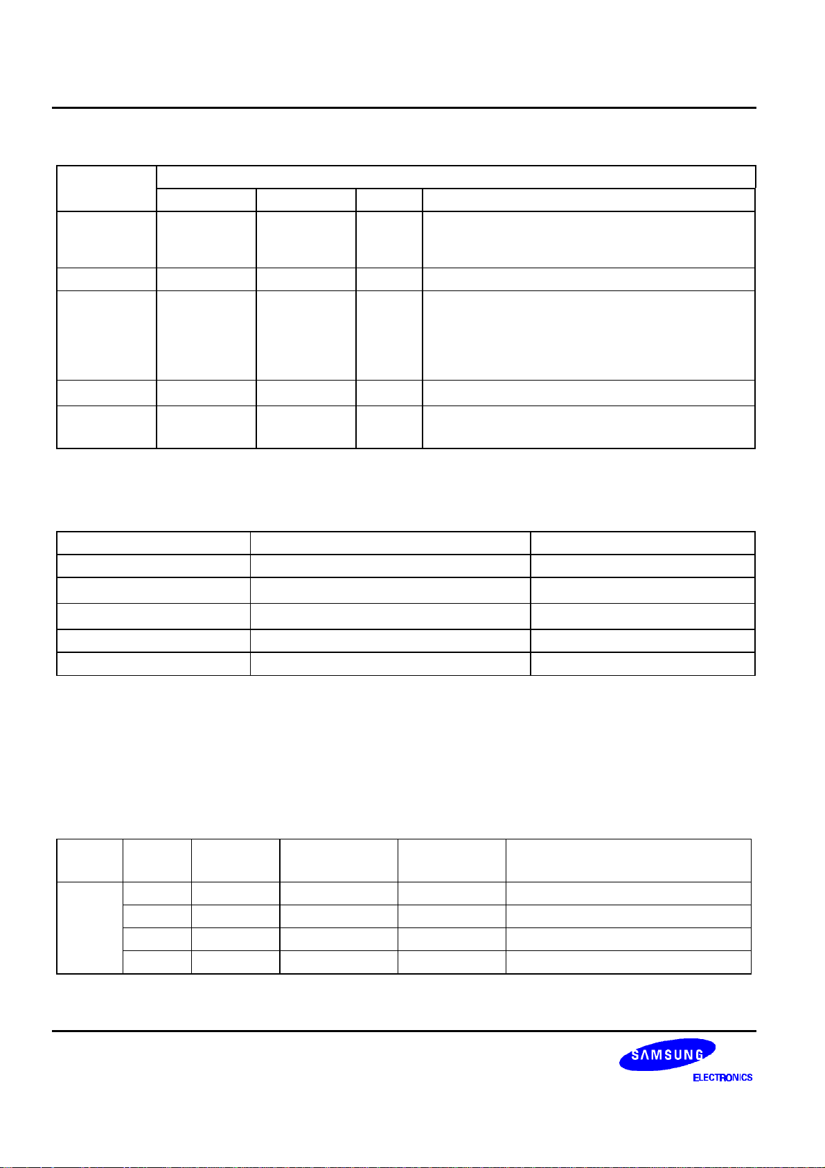
Table 16-1. Descriptions of Pins Used to Read/Write the EPROM
Main Chip During Programming
Pin Name Pin Name Pin No. I/O Function
P5.2 SDAT 22 I/O Serial data pin. Output port when reading and input
port when writing. Can be assigned as a Input /
push-pull output port.
P5.3 SCLK 23 I/O Serial clock pin. Input only pin.
TEST TEST 4 I Power supply pin for EPROM cell writing (indicates
that OTP enters into the writing mode). When 12.5
V is applied, OTP is in writing mode and when 5 V
is applied, OTP is in reading mode. (Option)
Hold GND when OTP is operating.
RESET RESET
VDD/V
SS
VDD/V
SS
8 I Chip initialization
24/1 –
Logic power supply pin. VDD should be tied to +5 V
during programming.
NOTE: ( ) means the 32-SOP OTP pin number.
Table 16-2. Comparison of S3P7544 and S3C7544 Features
Characteristic S3P7544 S3C7544
Program Memory 4 K-byte EPROM 4 K-byte mask ROM
Operating Voltage (VDD)
OTP Programming Mode
1.8 V (3 MHz) to 5.5 V 1.8 V (3 MHz) to 5.5 V
VDD = 5 V, V
(TEST) = 12.5 V
PP
–
Pin Configuration 24 SOP, 24 SDIP 24 SOP, 24 SDIP
EPROM Programmability User Program one time Programmed at the factory
OPERATING MODE CHARACTERISTICS
When 12.5 V is supplied to the VPP(TEST) pin of the S3P7544, the EPROM programming mode is entered. The
operating mode (read, write, or read protection) is selected according to the input signals to the pins listed in
Table 16-3 below.
Table 16-3. Operating Mode Selection Criteria
V
DD
V
PP
(TEST)
REG/
MEM
Address
(A15-A0)
R/W Mode
5 V 5 V 0 0000H 1 EPROM read
12.5 V 0 0000H 0 EPROM program
12.5 V 0 0000H 1 EPROM verify
12.5 V 1 0E3FH 0 EPROM read protection
NOTE: "0" means Low level; "1" means High level.
16-2
Page 22
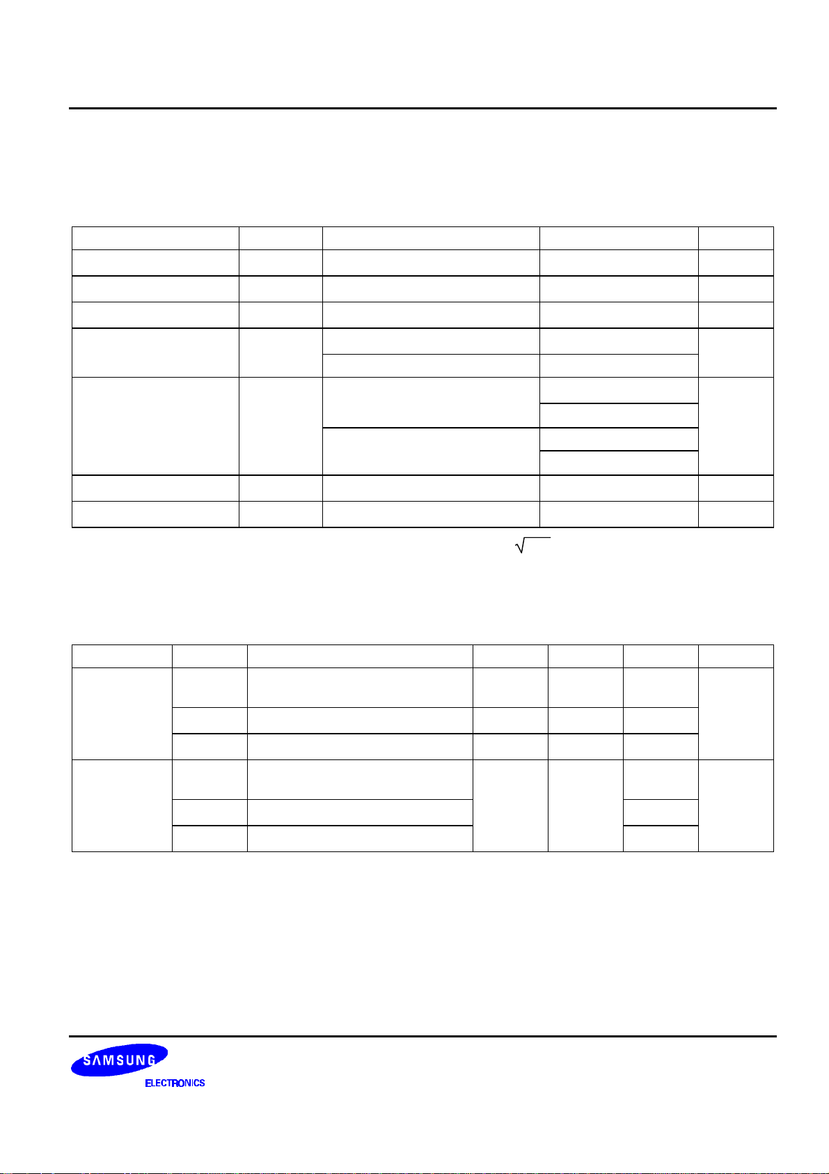
S3C7544/P7544 S3P7544 OTP
OTP ELECTRICAL DATA
Table 16-4. Absolute Maximum Ratings
(TA = 25 °C)
Parameter Symbol Conditions Rating Units
Supply Voltage
Input Voltage
Output Voltage
Output Current High
V
DD
I
V
V
OH
I
O
All I/O ports
One I/O port active – 5 mA
– – 0.3 to + 6.5 V
– 0.3 to V
–
– 0.3 to VDD + 0.3
DD
+ 0.3
V
V
All I/O ports active – 35
Output Current Low
I
OL
One I/O port active + 30 (peak) mA
(note)
+ 15
All I/O ports active + 100 (peak)
(note)
+ 60
Operating Temperature
Storage Temperature
T
A
T
stg
– – 40 to + 85
– – 65 to + 150
°
C
°
C
NOTE: The values for output current low (IOL) are calculated as peak value × Duty .
Table 16-5. D.C. Electrical Characteristics
(TA = – 40 °C to + 85 °C, VDD = 1.8 V to 5.5 V)
Parameter Symbol Conditions Min Typ Max Units
Input High
V
IH1
All input pins except V
IH2–VIH3
0.7 V
DD
–
V
DD
Voltage
Input Low
V
IH2
V
IH3
V
IL1
P0 and RESET
XIN and X
OUT
All input pins except V
IH2–VIH3
0.8 V
DD
V
– 0.1
DD
– –
–
–
V
DD
V
DD
0.3 V
DD
Voltage
V
IL2
V
IL3
P0 and RESET
XIN and X
OUT
0.2 V
0.1
DD
V
V
16-3
Page 23
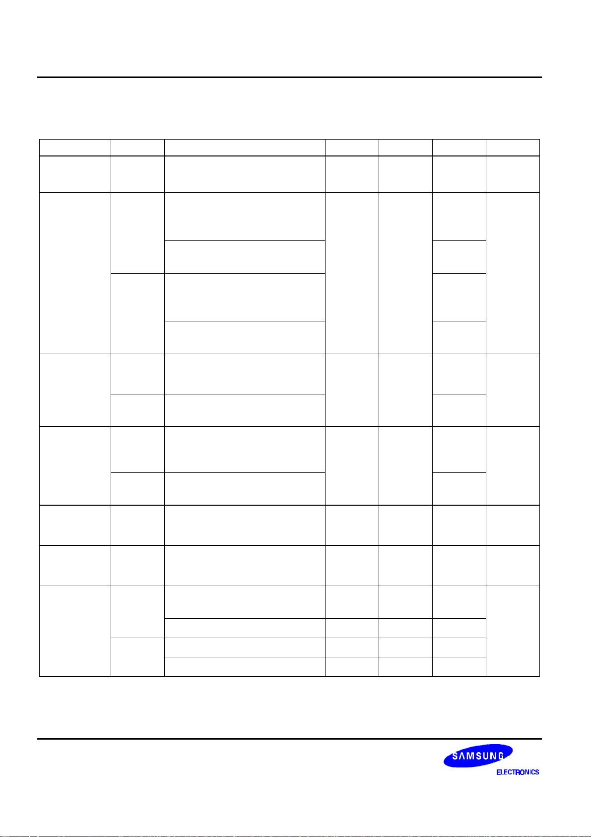
S3P7544 OTP S3C7544/P7544
Table 16-5. D.C. Electrical Characteristics (Continued)
(T
= – 40 °C to + 85 °C, VDD = 1.8 V to 5.5 V)
A
Parameter Symbol Conditions Min Typ Max Units
Output High
Voltage
V
OH
V
= 4.5 V to 5.5 V
DD
IOH = – 1 mA
V
DD
– 1.0
– – V
Output Low
Voltage
Input High
Leakage
Current
Input Low
Leakage
Current
Output High
Leakage
Current
Output Low
Leakage
Current
Pull-up
Resistor
V
V
I
LIH1
I
LIH2
I
LIL1
I
LIL2
I
LOH
I
LOL
R
R
OL1
OL2
L1
L2
V
= 4.5 V to 5.5 V
DD
IOL = 15 mA
Ports 4, 5
V
= 1.8 V to 5.5 V
DD
IOL = 1.6 mA
VDD = 4.5V to 5.5 V
I
= 4 mA
OL
All out ports except ports 4, 5
V
= 1.8 V to 5.5 V
DD
IOL = 1.6 mA
VIN = V
DD
All input pins except XIN and X
VIN = V
XIN and X
V
All input pins except XIN, X
= 0 V
IN
DD
OUT
OUT
and RESET
V
= 0 V
IN
XIN and X
VO = V
OUT
DD
All output pins
V
= 0 V
O
All output pins
V
= 5 V; V
DD
except
V
= 3 V
DD
V
= 5 V; V
DD
V
= 3 V
DD
= 0 V
I
RESET
= 0 V; RESET
I
OUT
– – 2 V
0.4
2
0.6
– – 3
20
– – – 3
– 20
– – 3
– – – 3
25 50 100
50 100 200
100 250 400
200 500 800
µA
µA
µA
µA
kΩ
16-4
Page 24
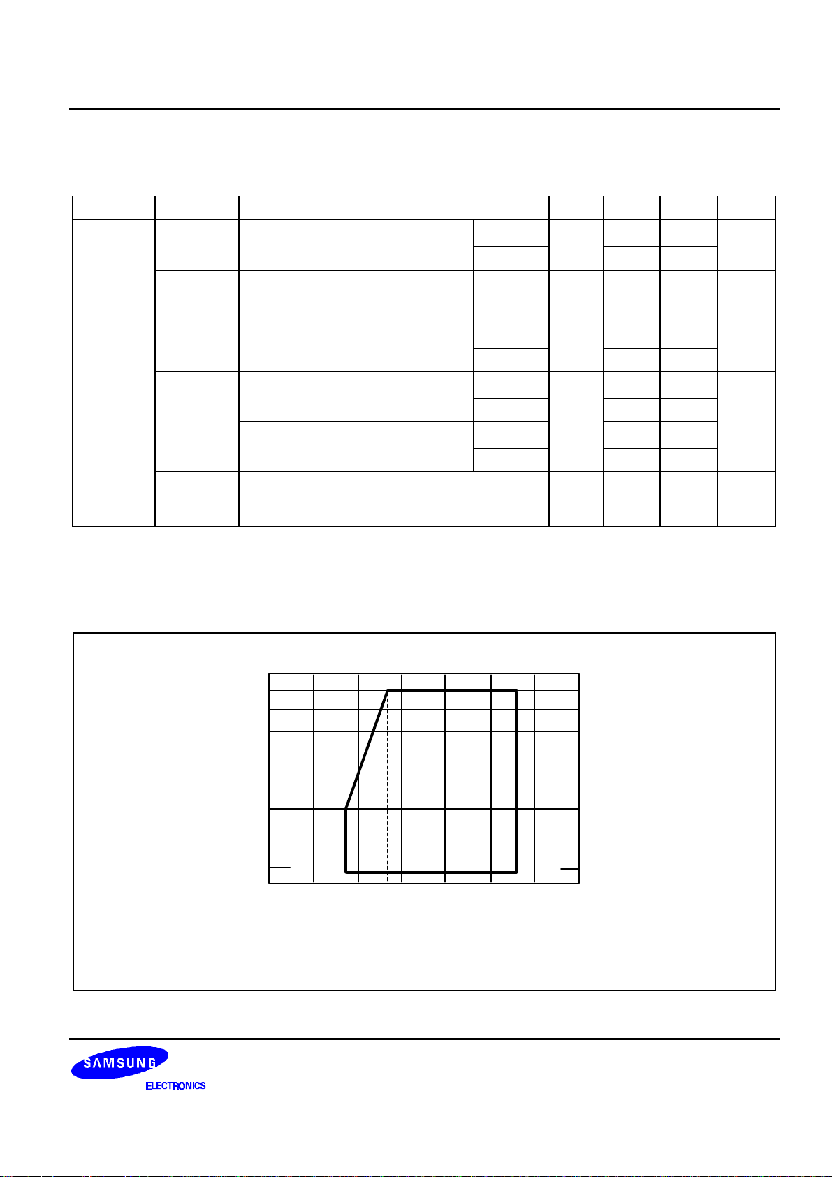
S3C7544/P7544 S3P7544 OTP
Table 16-5. D.C. Electrical Characteristics (Concluded)
(T
= – 40 °C to + 85 °C, VDD = 1.8 V to 5.5 V)
A
Parameter Symbol Conditions Min Typ Max Units
Supply
Current
I
DD1
(1)
(DAC on) Crystal oscillator; C1 = C2 = 22pF 4.19MHz 2.7 8.0
I
DD2
Run mode; V
Run mode; V
= 5.0 V ± 10%
DD
= 5.0 V ± 10%
DD
6.0MHz – 3.4 10.0
6.0MHz – 2.3 8.0
mA
mA
(DAC off) Crystal oscillator; C1 = C2 = 22pF 4.19MHz 1.7 5.5
V
= 3 V ± 10%
DD
6.0MHz 1.1 4.0
4.19MHz 0.8 3.0
I
DD3
Idle mode; V
= 5.0 V ± 10%
DD
6.0MHz – 0.7 2.5
mA
Crystal oscillator; C1 = C2 = 22pF 4.19MHz 0.5 1.8
V
= 3 V ± 10%
DD
6.0MHz 0.3 1.5
4.19MHz 0.2 1.0
I
DD4
Stop mode; V
Stop mode; V
= 5.0 V ± 10%
DD
= 3.0 V ± 10%
DD
– 0.2 3.0
0.1 2.0
µA
NOTES:
1. D.C. electrical values for supply current (I
resistors.
2. I
typical values are measured when DADATA register value is 055H .
DD1
CPU CLOCK
1.5 MHz
0.75 MHz
15.625 kHz
1 2
CPU CLOCK = 1/n x oscillator frequency (n = 4, 8 or 64)
DD1
1.8
to I
) do not include the current drawn through internal pull-up
DD3
2.7
3 4 5 6 7
SUPPLY VOLTAGE (V)
Main Osc. Freq.
6 MHz
3 MHz
400 kHz
Figure 16-2. Standard Operating Voltage Range
16-5
Page 25
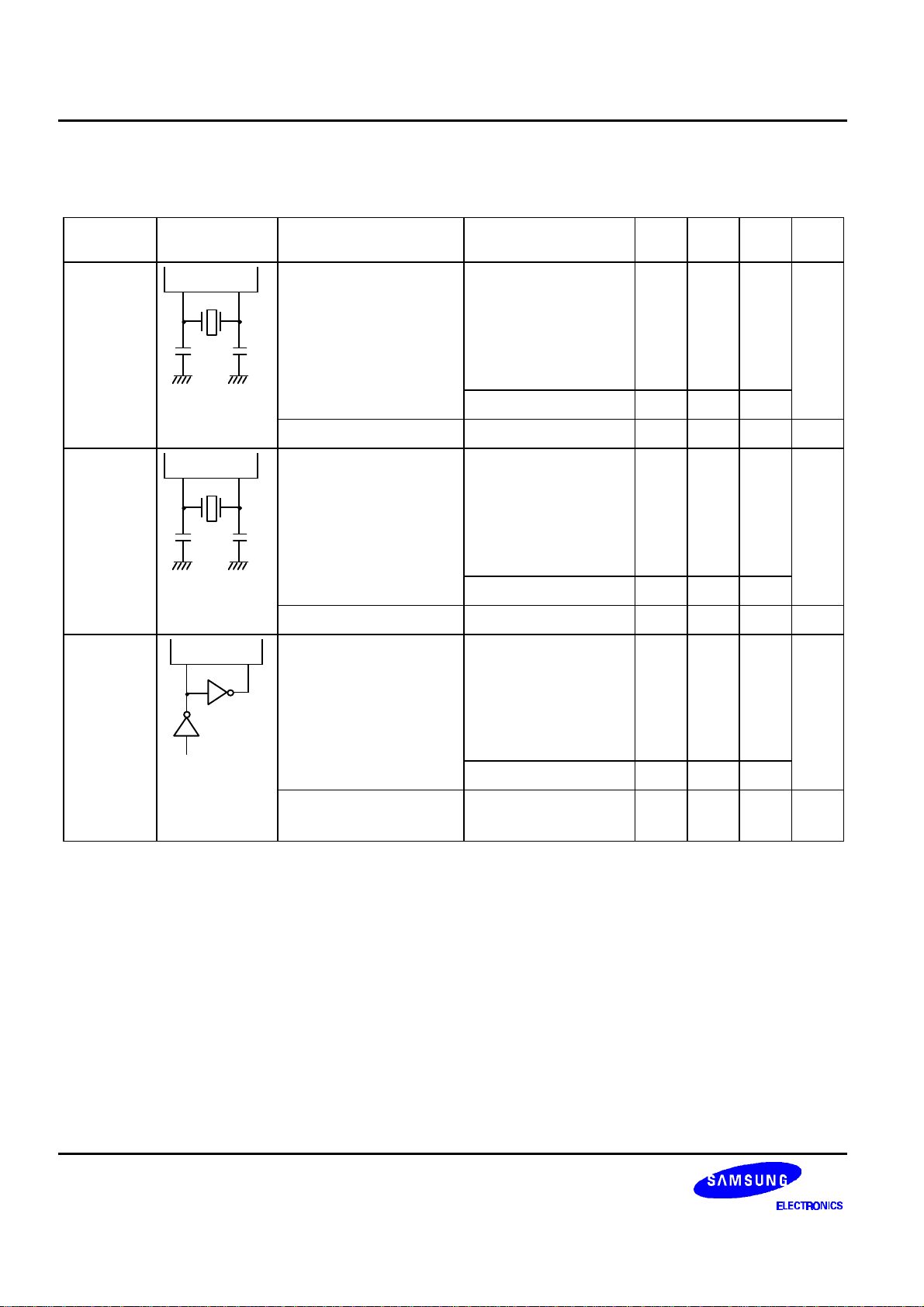
S3P7544 OTP S3C7544/P7544
Table 16-6. Oscillators Characteristics
(T
= – 40 °C + 85 °C, VDD = 1.8 V to 5.5 V)
A
Oscillator Clock
Configuration
Ceramic
Xin Xout
Oscillator
C1 C2
Crystal
Xin Xout
Oscillator
C1 C2
External
Xin Xout
Clock
Parameter Test Condition Min Typ Max Units
Oscillation frequency
Stabilization time
(2)
Oscillation frequency
Stabilization time
XIN input frequency
(2)
(1)
(1)
VDD = 2.7 V to 5.5 V
VDD = 1.8 V to 5.5 V
VDD = 3.0 V
(1)
VDD = 2.7 V to 5.5 V
VDD = 1.8 V to 5.5 V
VDD = 3.0 V
VDD = 2.7 V to 5.5 V
0.4 – 6.0 MHz
0.4 – 3
– – 4 ms
0.4 – 6.0 MHz
0.4 – 3
– – 10 ms
0.4 – 6.0 MHz
XIN input high and low
VDD = 1.8 V to 5.5 V
– 83.3 – 1250 ns
0.4 – 3
level width (tXH, tXL)
NOTES:
1. Oscillation frequency and XIN input frequency data are for oscillator characteristics only.
2. Stabilization time is the interval required for oscillating stabilization after a power-on occurs, or when stop mode is
terminated.
16-6
Page 26
S3C7544/P7544 S3P7544 OTP
Table 16-7. Input/Output Capacitance
(TA = 25 °C, V
DD
= 0 V )
Parameter Symbol Condition Min Typ Max Units
C
C
OUT
IN
f = 1 MHz; Unmeasured pins
are returned to V
SS
– – 15 pF
15 pF
Input
Capacitance
Output
Capacitance
I/O Capacitance
C
IO
15 pF
Table 16-8. Comparator Electrical Characteristics
(T
= – 40 °C to + 85 °C, VDD = 3.5 V to 5.5 V, VSS = 0 V)
A
Parameter Symbol Condition Min Typ Max Units
Resolution – – – – 8 bits
Absolute Accuracy – – 3 – 3 LSB
Differential Linearity Error DLE – 1 – 1 LSB
Setup Time
Output Resistance
t
su
R
O
– – 5
4.5 5 5.5
KΩ
µs
Table 16-9. A.C. Electrical Characteristics
(TA = – 40 °C to + 85 °C, V
= 1.8 V to 5.5 V)
DD
Parameter Symbol Conditions Min Typ Max Units
Instruction Cycle
t
CY
V
= 2.7 V to 5.5 V
DD
0.67 – 64
Time
TCL0 Input
VDD = 1.8 V to 5.5 V
f
TI
V
= 2.7 V to 5.5 V
DD
1.33
0 – 1.5 MHz
Frequency
TCL0 Input High,
t
TIH,
VDD = 1.8 V to 5.5 V
t
TIL
V
= 2.7 V to 5.5 V
DD
0.48 – –
1 MHz
Low Width
Interrupt Input
t
INTH, tINTL
VDD = 1.8 V to 5.5 V
INT0, INT1, KS0–KS1 10 – –
1.8
High, Low Width
RESET Input Low
t
RSL
Input – – 10
Width
µs
µs
µs
µs
16-7
Page 27
S3P7544 OTP S3C7544/P7544
Table 16-10. RAM Data Retention Supply Voltage in Stop Mode
(TA = – 40 °C to + 85 °C)
Parameter Symbol Conditions Min Typ Max Unit
Data retention supply voltage
Data retention supply current
V
DDDR
I
DDDR
V
DDDR
– 1.8 – 5.5 V
= 1.8 V
– 0.1 10
µA
Release signal set time
Oscillator stabilization wait
(1)
time
NOTES:
1. During oscillator stabilization wait time, all CPU operations must be stopped to avoid instability during oscillator
start-up.
2. Use the basic timer mode register (BMOD) interval timer to delay the execution of CPU instructions during the wait time.
t
SREL
t
WAIT
– 0 – –
Released by RESET
Released by interrupt –
µs
–
217/fx
(2)
– ms
– ms
16-8
 Loading...