

Page 1
RFF70N06
Data Sheet March 1999
25A, 60V, 0.025 Ohm, N-Channel Power
MOSFET
The RFF70N06 N-Channel powerMOSFETismanufactured
using the MegaFET process. This process, which uses
feature sizes approaching those of LSI circuits gives
optimum utilization of silicon, resulting in outstanding
performance. It was designed for use in applications such as
switching regulators, switching converters, motor drivers,
and relay drivers. These transistors can be operated directly
from integrated circuits.
Reliability screening is available as either commercial or
TX/TXV equivalent of MIL-S-19500. Contact Intersil
Corporation High-Reliability Marketing group for any desired
deviations from the data sheet.
Formerly developmental type TA49007.
Ordering Information
PART NUMBER PACKAGE BRAND
RFF70N06 TO-254AA RFF70N06
NOTE: When ordering, use the entire part number.
File Number
Features
• 25A†, 60V
DS(ON)
= 0.025Ω
•r
• Temperature Compensating PSPICE™ Model
• Peak Current vs Pulse Width Curve
• UIS Rating Curve
o
C Operating Temperature
• 150
• Reliability Screened
Current is limited by the package capability.
†
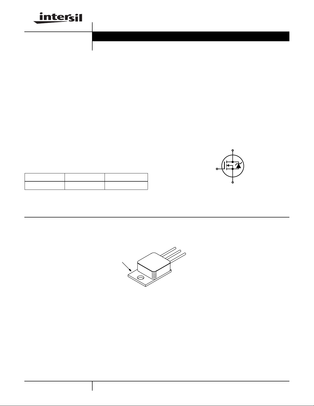
Symbol
D
G
S
4073.2
Commercial Version: RFG70N06.
Packaging
JEDEC TO-254AA
GATE
PACKAGE TAB
(ISOLATED)
CAUTION: Berylia Warning per MIL-S-19500.
Refer to package specifications.
SOURCE
DRAIN
4-442
CAUTION: These devices are sensitive to electrostatic discharge; follow proper ESD Handling Procedures.
PSPICE™ is a trademark of MicroSim Corporation.
http://www.intersil.com or 407-727-9207
| Copyright © Intersil Corporation 1999
Page 2
RFF70N06
Absolute Maximum Ratings T
= 25oC, Unless Otherwise Specified
C
RFF70N06 UNITS
Drain to Source Voltage (Note 1). . . . . . . . . . . . . . . . . . . . . . . . . . . . . . . . . . . . . . . V
Drain to Gate Voltage (RGS = 20kΩ) (Note 1) . . . . . . . . . . . . . . . . . . . . . . . . . . . . . V
Gate to Source Voltage . . . . . . . . . . . . . . . . . . . . . . . . . . . . . . . . . . . . . . . . . . . . . . . V
Continuous Drain Current (Note 2) . . . . . . . . . . . . . . . . . . . . . . . . . . . . . . . . . . . . . . . . I
Pulsed Drain Current (Note 4) (Figure 5). . . . . . . . . . . . . . . . . . . . . . . . . . . . . . . . . . . I
Single Pulse Avalanche Rating (Figure 6). . . . . . . . . . . . . . . . . . . . . . . . . . . . . . . . . .E
Power Dissipation . . . . . . . . . . . . . . . . . . . . . . . . . . . . . . . . . . . . . . . . . . . . . . . . . . . . .P
DSS
DGR
GS
DM
AS
D
Refer to Peak Current Curve
D
Linear Derating Factor. . . . . . . . . . . . . . . . . . . . . . . . . . . . . . . . . . . . . . . . . . . . . . . . . . . .
Operating and Storage Temperature . . . . . . . . . . . . . . . . . . . . . . . . . . . . . . . . . .TJ, T
STG
Maximum Temperature for Soldering
Leads at 0.063in (1.6mm) from Case for 10s. . . . . . . . . . . . . . . . . . . . . . . . . . . . . . . T
CAUTION: Stresses above those listed in “Absolute Maximum Ratings” may cause permanent damage to the device. This is a stress only rating and operationofthe
device at these or any other conditions above those indicated in the operational sections of this specification is not implied.
L
60 V
60 V
±20 V
25 (Note 2)
Refer to UIS Curve
100
0.80
-55 to 150
260
A
W
W/oC
o
C
o
C
NOTE:
1. TJ= 25oC to 125oC.
2. Current is limited by the package capability.
Electrical Specifications T
= 25oC, Unless Otherwise Specified
C
PARAMETER SYMBOL TEST CONDITIONS MIN TYP MAX UNITS
Drain to Source Breakdown Voltage BV
Gate Threshold Voltage V
GS(TH)VGS
Zero Gate Voltage Drain Current I
Gate to Source Leakage Current I
Drain to Source On Resistance (Note 3) r
DS(ON)ID
Turn-On Time t
Turn-On Delay Time t
d(ON)
Rise Time t
Turn-Off Delay Time t
d(OFF)
Fall Time t
Turn-Off Time t
Total Gate Charge Q
g(TOT)VGS
Gate Charge at 10V Q
Threshold Gate Charge Q
Input Capacitance C
Output Capacitance C
Reverse Transfer Capacitance C
Thermal Resistance Junction to Case R
Thermal Resistance Junction to Ambient R
DSSID
DSS
GSS
ON
r
f
OFF
g(10)
g(TH)
ISS
OSS
RSS
θJC
θJA
= 250µA, VGS = 0V 60 - - V
= VDS, ID = 250µA 2.0 3.0 4.5 V
VDS = Rated BV
DSS, VGS
VDS= 0.8 x Rated BV
= 0V - - 25 µA
DSS,VGS
= 0V, TC= 125oC - - 250 µA
VGS = ±20V, TC = 125oC--±100 µΑ
= 25A, VGS = 10V - - 0.025 Ω
VDD = 30V, I
VGS = 10V, RGS = 2.35Ω
(Figures 13, 16, 17)
≈ 25A, R
D
= 1.2Ω,
L
- - 240 ns
-2570 ns
- 70 170 ns
- 60 150 ns
-2565 ns
- - 215 ns
= 0 to 20V VDD = 30V, ID = 25A,
VGS = 0 to 10V - - 145 nC
VGS = 0 to 2V - - 7 nC
RL = 1.2Ω
I
= 1.0mA
G(REF)
(Figures 18, 19)
VDS = 25V, VGS = 0V, f = 1MHz
(Figure 12)
- - 260 nC
- 3100 - pF
- 900 - pF
- 300 - pF
- - 1.25
o
C/W
--48oC/W
Source to Drain Diode Specifications
PARAMETER SYMBOL TEST CONDITIONS MIN TYP MAX UNITS
Source to Drain Diode Voltage V
Diode Reverse Recovery Time t
SD
rr
NOTES:
3. Pulse test: pulse width ≤ 300ms, duty cycle ≤ 2%.
4. Repetitive rating: pulse width is limited by maximum junction temperature. See Transient Thermal Impedance curve Figure 3).
4-443
ISD = 25A - 1.1 1.5 V
ISD = 25A, dISD/dt = 100A/µs - 190 300 ns
Page 3
RFF70N06
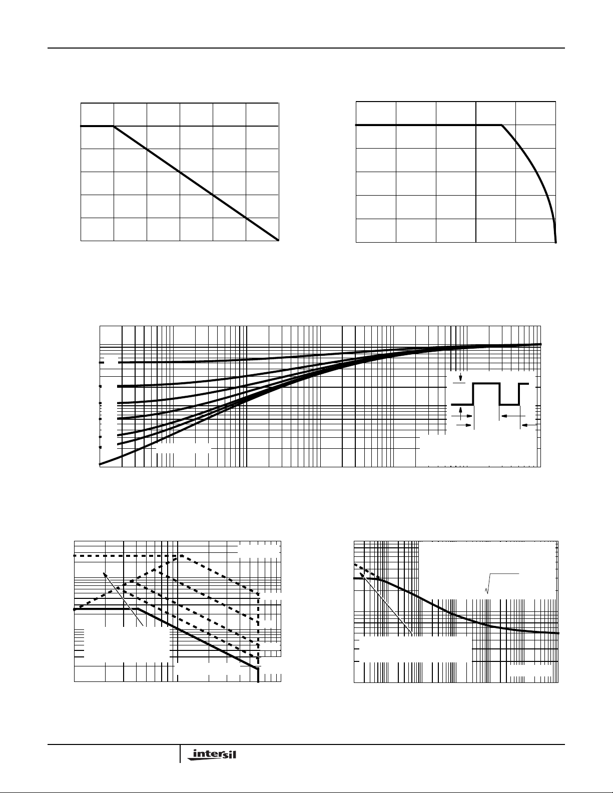
Typical Performance Curves
1.2
1.0
0.8
0.6
0.4
0.2
POWER DISSIPATION MULTIPLIER
0
0 25 50 75 100 125 150
TC, CASE TEMPERATURE (oC) TC, CASE TEMPERATURE (oC)
Unless Otherwise Specified
FIGURE 1. NORMALIZED POWER DISSIPATION vs CASE
TEMPERATURE
2
1
30
25
20
15
10
, DRAIN CURRENT (A)
D
I
5
0
100755025
125
FIGURE 2. MAXIMUM CONTINUOUS DRAIN CURRENT vs
CASE TEMPERATURE
150
0.5
0.2
0.1
0.1
, NORMALIZED
Z
500
100
10
, DRAIN CURRENT (A)
D
I
1
0.05
JC
θ
THERMAL IMPEDANCE
0.02
0.01
0.01
-5
10
OPERATION IN THIS
AREA MAY BE
LIMITED BY r
1
V
SINGLE PULSE
-4
10
FIGURE 3. NORMALIZED MAXIMUM TRANSIENT THERMAL IMPEDANCE
DS(ON)
V
MAX = 60V
DSS
, DRAIN TO SOURCE VOLTAGE (V)
DS
10 100
-3
10
t, RECTANGULAR PULSE DURATION (s)
TC = 25oC
100µs
1ms
10ms
100ms
DC
-2
10
3
10
2
10
, PEAK CURRENT (A)
DM
I
1
10
10
NOTES:
DUTY FACTOR: D = t
PEAK TJ = PDM x Z
-1
10
FOR TEMPERATURES ABOVE 25oC
DERATE PEAK CURRENT
CAPABILITY AS FOLLOWS:
TRANSCONDUCTANCE
MAY LIMIT CURRENT
IN THIS REGION V
-5
-4
10
10
P
DM
0
10
=
II
25
= 10V
GS
-3
t, PULSE WIDTH (s)
-2
10
t
1
t
2
1/t2
x R
JC
θ
150 T
--------------------- -
-1
10
θ
–
125
+ T
JC
C
10
C
TC = 25oC
0
10
1
1
10
FIGURE 4. FORWARD BIAS SAFE OPERATING AREA FIGURE 5. PEAK CURRENT CAPABILITY
4-444
Page 4

RFF70N06
Typical Performance Curves
300
100
75
10
, AVALANCHE CURRENT (A)
If R = 0
AS
I
tAV = (L) (IAS) / (1.3 RATED BV
If R ≠ 0
tAV = (L/R) ln [(IAS*R) / (1.3 RATED BV
1
0.01
0.1 1 10 100
t
STARTING TJ = 150oC
DSS
, TIME IN AVALANCHE (ms)
AV
Unless Otherwise Specified (Continued)
STARTING TJ = 25oC
- VDD)
- VDD) + 1]
DSS
NOTE: Refer to Intersil Application Notes AN9321 and AN9322.
FIGURE 6. UNCLAMPED INDUCTIVE SWITCHING
150
VDD = 15V
PULSE DURATION = 250µs
125
DUTY CYCLE = 0.5% MAX
100
75
50
, DRAIN TO SOURCE CURRENT (A)
25
DS(ON)
0
I
0
2 4 6
V
GS
, GATE TO SOURCE VOLTAGE (V)
-55oC
25oC
150oC
1000
150
VGS = 10V
VGS = 20V
125
100
75
50
, DRAIN CURRENT (A)
D
I
25
0
024 6810
VDS, DRAIN TO SOURCE VOLTAGE (V)
250µs PULSE TEST
TC = 25oC
VGS = 4.5V
VGS = 7V
VGS = 6V
VGS = 5V
FIGURE 7. SATURATION CHARACTERISTICS
2.5
PULSE DURATION = 250µs
V
= 10V,
GS
= 25A
I
D
2.0
1.5
1.0
ON RESISTANCE
0.5
NORMALIZED DRAIN TO SOURCE
8
0
-80 -40 0 40 80
T
, JUNCTION TEMPERATURE (oC)
J
120
160
FIGURE 8. TRANSFER CHARACTERISTICS FIGURE 9. NORMALIZED DRAIN TOSOURCE ON
2.0
VGS = VDS, ID = 250µA
1.5
1.0
NORMALIZED GATE
0.5
THRESHOLD VOLTAGE
0
-80 -40 0 40 80 160120
TJ, JUNCTION TEMPERATURE (oC)
FIGURE 10. NORMALIZED GATETHRESHOLD VOLTAGE vs
JUNCTION TEMPERATURE
4-445
RESISTANCE vs JUNCTION TEMPERATURE
2.0
ID = 250µA
1.5
1.0
0.5
BREAKDOWN VOLTAGE
NORMALIZED DRAIN TO SOURCE
0
-80 -40 0 40 80 120 160
TJ, JUNCTION TEMPERATURE (oC)
FIGURE 11. NORMALIZED DRAIN TO SOURCE BREAKDOWN
VOLTAGE vs JUNCTION TEMPERATURE
Page 5

RFF70N06
Typical Performance Curves
Unless Otherwise Specified (Continued)
5000
VGS = 0V, f = 0.1MHz
4000
C
C
ISS
RSS
OSS
= C
≈ CDS + C
GD
GD
GS
= CGS + C
C
3000
2000
C, CAPACITANCE (pF)
1000
0
0
510152025
VDS, DRAIN TO SOURCE VOLTAGE (V)
FIGURE 12. CAPACITANCE vs DRAIN TO SOURCE VOLTAGE
Test Circuits and Waveforms
V
DS
L
VARY t
TO OBTAIN
P
REQUIRED PEAK I
V
GS
AS
R
G
DUT
+
-
60
45
30
15
, DRAIN TO SOURCE VOLTAGE (V)
DS
V
0
VDD = BV
I
G(REF)
20
I
G(ACT)
DSS
0.75 BV
0.50 BV
0.25 BV
RL = 1.2Ω
I
= 1.0mA
G(REF)
V
= 10V
GS
DSS
DSS
DSS
t, TIME (µs)
0.75 BV
0.50 BV
0.25 BV
VDD = BV
DSS
DSS
DSS
I
80
I
DSS
G(REF)
G(ACT)
10.0
7.5
5.0
2.5
0
, GATE TO SOURCE VOLTAGE (V)
GS
V
NOTE: Refer to Intersil Application Notes AN7254 and AN7260.
FIGURE 13. NORMALIZED SWITCHING WAVEFORMSFOR
CONSTANT GATE CURRENT
BV
DSS
t
P
I
AS
V
DD
V
DS
V
DD
0V
P
I
AS
0.01Ω
0
t
AV
t
FIGURE 14. UNCLAMPED ENERGY TEST CIRCUIT FIGURE 15. UNCLAMPED ENERGY WAVEFORMS
t
ON
t
10%
d(ON)
90%
50%
t
10%
r
PULSE WIDTH
V
DS
V
DS
R
DUT
L
+
V
DD
-
0
V
GS
0
V
GS
R
GS
V
GS
t
d(OFF)
90%
FIGURE 16. SWITCHING TIME TEST CIRCUIT FIGURE 17. RESISTIVE SWITCHING WAVEFORMS
t
OFF
50%
t
f
90%
10%
4-446
Page 6

RFF70N06
Test Circuits and Waveforms
V
DS
V
GS
I
g(REF)
FIGURE 18. GATE CHARGE TEST CIRCUIT FIGURE 19. GATE CHARGE WAVEFORMS
(Continued)
R
L
DUT
+
V
DD
-
Data Packages - Intersil Power Transistors
TX and TXV Equivalents
1. TX/TXV Equivalent - Standard Data Package
Certificate of Compliance
A.
Assembly Flow Chart
B.
Preconditioning
C.
Group A
D.
Group B
E.
Group C
F.
2. TX/TXV Equivalent - Optional Data Package
Certificate of Compliance
A.
Assembly Flow Chart
B.
Preconditioning
C.
Group A
D.
Group B
E.
Group C
F.
- Attributes Data Sheet
- Attributes Data Sheet
- Attributes Data Sheet
- Attributes Data Sheet
- Attributes Data Sheet
- Precondition Lot Traveler
- Pre and Post Burn-In Read and Record Data
- Attributes Data Sheet
- Group A Lot Traveler
- Attributes Data Sheet
- Group B Lot Traveler
- Pre and Post Read and Record Data for Intermittent
Operating Life (Subgroup B3)
- Bond Strength Data (Subgroup B3)
- Pre and Post High Temperature Operating Life
Read and Record Data (Subgroup B6)
- Attributes Data Sheet
- Group C Lot Traveler
- Pre and Post Read and Record Data for Intermittent
Operating Life (Subgroup C6)
- Bond Strength Data (Subgroup C6)
V
DD
VGS= 2V
0
I
g(REF)
0
Q
g(TOT)
V
DS
Q
g(10)
V
GS
Q
g(TH)
VGS = 10V
VGS= 20V
4-447
Page 7

PSPICE Electrical Model
SUBCKT RFF70N06 2 1 3 ; rev 5/29/95
CA 12 8 5.20e-9
CB 15 14 5.20e-9
CIN 6 8 2.80e-9
DBODY 7 5 DBDMOD
DBREAK 5 11 DBREAKMOD
DPLCAP 10 5 DPLCAPMOD
EBREAK 11 7 17 18 68.7
EDS 14 8 5 8 1
EGS 13 8 6 8 1
ESG 6 10 6 8 1
EVTHRESH 6 21 19 8 1
EZTEMPCO 20 6 18 22 1
IT 8 17 1
LDRAIN 2 5 1e-9
LGATE 1 9 6.04e-9
LSOURCE 3 7 2.24e-9
MOS1 16 6 8 8 MSTRONG M = 0.99
MOS2 16 21 8 8 MWEAK M = 0.01
RBREAK 17 18 RBREAKMOD 1
RDRAIN 50 16 RDRAINMOD 8.03e-3
RGATE 9 20 1
RIN 6 8 1e9
RLDRAIN 2 5 10
RLGATE 1 9 60.4
RLSOURCE 3 7 22.4
RSCL1 5 51 RSCLMOD 1e-6
RSCL2 5 50 1e3
RSOURCE 8 7 RSOURCEMOD 7.20e-3
RTHRESH 22 8 RTHRESMOD 1
RZTEMPCO 18 19 RZTEMPCOMOD 1
S1A 6 12 13 8 S1AMOD
S1B 13 12 13 8 S1BMOD
S2A 6 15 14 13 S2AMOD
S2B 13 15 14 13 S2BMOD
GATE
1
LGATE
RLGATE
RFF70N06
EZTEMPCO
9
20
RGATE
12
+
S1A
S1B
CA
ESG
18
22
10
+
13814
EGS
6
8
RSCL2
6
RIN
13
+
6
8
DPLCAP
EVTHRESH
+
19
8
CIN
S2A
15
S2B
CB
13
EDS
16
+
5
5
51
5
8
RSCL1
51
+
ESCL
50
RDRAIN
21
MOS1
14
8
DBREAK
EBREAK
MOS2
RSOURCE
17
11
17
18
LDRAIN
RLDRAIN
+
DBODY
LSOURCE
7
RLSOURCE
RBREAK
RZTEMPCO
IT
RTHRESH
DRAIN
2
3
SOURCE
18
19
VBAT
+
22
VBAT 22 19 DC 1
ESCL 51 50 VALUE = {(V(5,51)/ABS(V(5,51)))*(PWR(V(5,51)/(1e-6*250),3))}
.MODEL DBDMOD D (IS = 1e-12 RS = 11.01e-3 TRS1 = 1.75e-3 TRS2 = -0.06e-6 CJO = 2.70e-9 TT = 7.82e-8 M = 0.45)
.MODEL DBREAKMOD D (RS = 88e-3 TRS1 = 1.50e-3 TRS2 = 0)
.MODEL DPLCAPMOD D (CJO = 2.60e-9 IS = 1e-30 N = 10 M=0.7)
.MODEL MSTRONG NMOS (VTO = 3.85 KP = 47.2 IS = 1e-30 N = 10 TOX = 1L = 1u W = 1u)
.MODEL MWEAK NMOS (VTO = 3.09 KP = 47.2 IS = 1e-30 N = 10 TOX = 1L = 1u W = 1u)
.MODEL RBREAKMOD RES (TC1 = 1e-3 TC2 = 0)
.MODEL RDRAINMOD RES (TC1 = 7e-3 TC2 = 1.90e-5)
.MODEL RDSOURCEMOD RES (TC1 = 1e-3 TC2 = 1e-6)
.MODEL RSCLMOD RES (TC1 = 0 TC2 = 0)
.MODEL RTHRESHMOD RES (TC1 = -3.10e-3 TC2 = -1e-5)
.MODEL RZTEMPCOMOD RES (TC1 = -2.25e-3 TC2 = -5.75e-7)
.MODEL S1AMOD VSWITCH (RON = 1e-5 ROFF = 0.1 VON = -6.0 VOFF= -4.0)
.MODEL S1BMOD VSWITCH (RON = 1e-5 ROFF = 0.1 VON = -4.0 VOFF= -6.0)
.MODEL S2AMOD VSWITCH (RON = 1e-5 ROFF = 0.1 VON = -2.0 VOFF= 2.0)
.MODEL S2BMOD VSWITCH (RON = 1e-5 ROFF = 0.1 VON = 2.0 VOFF= -2.0)
.ENDS
NOTE: For further discussion of the PSPICE model, consult A New PSPICE Sub-Circuit for the Power MOSFET Featuring Global
Temperature Options; IEEE Power Electronics Specialist Conference Records, 1991.
4-448
Page 8

RFF70N06
Screening Information
Screening is performed in accordance with the latest revision in effect of MIL-S-19500, (Screening Information Table)
.
Delta Tests and Limits (JANTX/JANTXV Equivalent)
PARAMETER SYMBOL TEST CONDITIONS MAX UNITS
Gate to Source Leakage Current
Zero Gate Voltage Drain Current
On Resistance
Gate Threshold Voltage
I
GSS
I
DSS
r
DS(ON)
V
GS(TH)
NOTES:
5. Or 100% of Initial Reading (whichever is greater).
6. Of Initial Reading.
Screening Information
TEST JANTX/JANTXV EQUIVALENT
Gate Stress VGS = 30V, t = 250µs
Pind Optional
PDA 10%
Pre Burn-In Test (Note 7) MIL-S-19500 Group A, Subgroup 2 (All Static Tests at 25
Steady State Gate Bias (Gate Stress) MIL-STD-750, Method 1042, Condition B
Interim Electrical Tests (Note 7) All Delta Parameters Listed in the Delta Tests and Limits Table
Steady State Reverse Bias (Drain Stress) MIL-STD-750, Method 1042, Condition A
Final Electrical Tests (Note 7) MIL-S-19500, Group A, Subgroup 2
NOTE:
7. Test limits are identical pre and post burn-in.
VGS = ±20V, TC = 25oC
VDS = 80% Rated Value, TC = 25oC
TC = 125oC at Rated I
ID = 1.0mA, TC = 25oC
= 80% of Rated Value,
V
GS
= 150oC, Time = 48 hours
T
A
= 80% of Rated Value,
V
DS
= 150oC, Time = 168 hours
T
A
D
±20(Note 5) nA
±25(Note 5) µA
±20% (Note 6) Ω
±20% (Note 6) V
o
C)
Additional Screening Tests
PARAMETER SYMBOL TEST CONDITIONS MAX UNITS
Safe Operating Area
Unclamped Inductive Switching
Thermal Response
Thermal Impedance
SOA
I
∆V
∆V
AS
SD
SD
VDS = 48V, t = 10ms
V
GS(PEAK)
tH = 100ms; VH = 25V, IH = 4A
tH = 500ms; VH = 25V, IH = 4A
= 15V, L = 0.1mH
4.8 A
75 A
220 mV
330 mV
All Intersil semiconductor products are manufactured, assembled and tested under ISO9000 quality systems certification.
Intersil semiconductor products are sold by description only. Intersil Corporation reserves the right to make changes in circuit design and/or specifications at any time without notice. Accordingly,the reader is cautioned to verify that data sheets are current before placing orders. Information furnished by Intersil is believed to be accurate and
reliable. However, no responsibility is assumed by Intersil or its subsidiaries for its use; nor for any infringements of patents or other rights of third parties which may result
from its use. No license is granted by implication or otherwise under any patent or patent rights of Intersil or its subsidiaries.
For information regarding Intersil Corporation and its products, see web site http://www.intersil.com
Sales Office Headquarters
NORTH AMERICA
Intersil Corporation
P. O. Box 883, Mail Stop 53-204
Melbourne, FL 32902
TEL: (407) 724-7000
FAX: (407) 724-7240
4-449
EUROPE
Intersil SA
Mercure Center
100, Rue de la Fusee
1130 Brussels, Belgium
TEL: (32) 2.724.2111
FAX: (32) 2.724.22.05
ASIA
Intersil (Taiwan) Ltd.
7F-6, No. 101 Fu Hsing North Road
Taipei, Taiwan
Republic of China
TEL: (886) 2 2716 9310
FAX: (886) 2 2715 3029
 Loading...