

Page 1
RFD8P05, RFD8P05SM, RFP8P05
Data Sheet July 1999
8A, 50V, 0.300 Ohm, P-Channel Power
MOSFETs
These products are P-Channel power MOSFETs
manufactured using the MegaFET process. This process,
which uses feature sizes approaching those of LSI circuits,
gives optimum utilization of silicon, resulting in outstanding
performance. They were designed for use in applications
such as switching regulators, switching converters, motor
drivers, and relay drivers. These transistors can be operated
directly from integrated circuits.
Formerly developmental type TA09832.
Ordering Information
PART NUMBER PACKAGE BRAND
RFD8P05 TO-251AA D8P05
RFD8P05SM TO-252AA D8P05
RFP8P05 TO-220AB RFP8P05
NOTE: Whenordering, use theentirepart number.Addthe suffix9A
to obtain the TO-252AA variant in tape and reel, i.e.,
RFD8P05SM9A.
File Number
Features
• 8A, 50V
DS(ON)
= 0.300Ω
•r
• UIS SOA Rating Curve
• SOA is Power Dissipation Limited
• Nanosecond Switching Speeds
• Linear Transfer Characteristics
• High Input Impedance
• Related Literature
- TB334 “Guidelines for Soldering Surface Mount
Components to PC Boards”
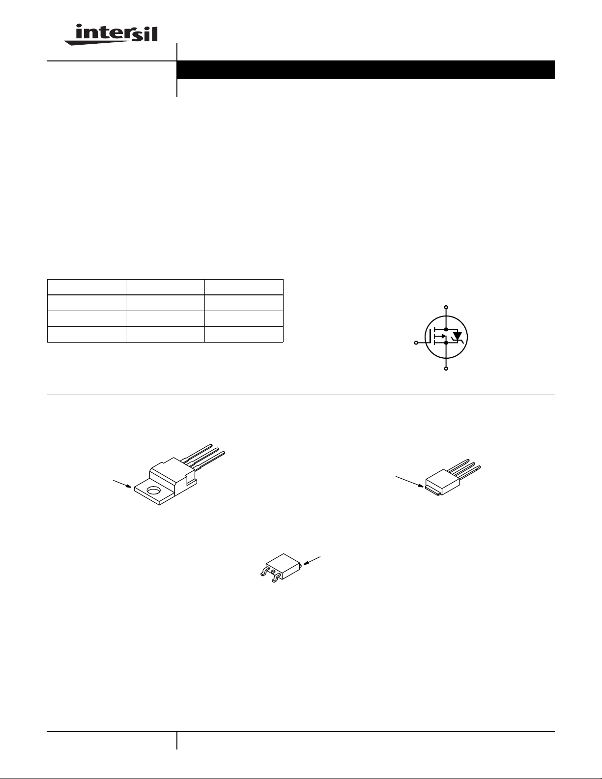
Symbol
D
G
S
2384.2
Packaging
DRAIN (FLANGE)
JEDEC TO-220AB JEDEC TO-251AA
SOURCE
DRAIN
GATE
DRAIN (FLANGE)
JEDEC TO-252AA
DRAIN (FLANGE)
GATE
SOURCE
SOURCE
DRAIN
GATE
4-112
CAUTION: These devices are sensitive to electrostatic discharge; follow proper ESD Handling Procedures.
http://www.intersil.com or 407-727-9207
| Copyright © Intersil Corporation 1999.
Page 2
RFD8P05, RFD8P05SM, RFP8P05
Absolute Maximum Ratings T
= 25oC Unless Otherwise Specified
C
RFD8P05,
RFD8P05SM, RFP8P05 UNITS
Drain to Source Voltage (Note 1). . . . . . . . . . . . . . . . . . . . . . . . . . . . . . . . . . . . . . . . . . . . . V
Drain to Gate Voltage (RGS = 20KΩ) (Note 1). . . . . . . . . . . . . . . . . . . . . . . . . . . . . . . . . . .V
DSS
DGR
Continuous Drain Current . . . . . . . . . . . . . . . . . . . . . . . . . . . . . . . . . . . . . . . . . . . . . . . . . . . . .I
Pulsed Drain Current (Note 3) . . . . . . . . . . . . . . . . . . . . . . . . . . . . . . . . . . . . . . . . . . . . . . . . I
Gate to Source Voltage . . . . . . . . . . . . . . . . . . . . . . . . . . . . . . . . . . . . . . . . . . . . . . . . . . . . .V
Maximum Power Dissipation . . . . . . . . . . . . . . . . . . . . . . . . . . . . . . . . . . . . . . . . . . . . . . . . . . P
D
DM
GS
D
-50 V
-50 V
-8 A
-20 A
±20 V
48 W
Dissipation Derating Factor . . . . . . . . . . . . . . . . . . . . . . . . . . . . . . . . . . . . . . . . . . . . . . . . . . . . . 0.27 W/oC
Single Pulse Avalanche Energy Rating . . . . . . . . . . . . . . . . . . . . . . . . . . . . . . . . . . . . . . . . . E
Operating and Storage Temperature . . . . . . . . . . . . . . . . . . . . . . . . . . . . . . . . . . . . . . . TJ,T
AS
STG
Maximum Temperature for Soldering
Leads at 0.063in (1.6mm) from Case for 10s. . . . . . . . . . . . . . . . . . . . . . . . . . . . . . . . . . . . T
Package Body for 10s, See Techbrief 334 . . . . . . . . . . . . . . . . . . . . . . . . . . . . . . . . . . . . .T
CAUTION: Stresses above those listed in “Absolute Maximum Ratings” may cause permanent damage to the device. This is a stress only rating and operationofthe
device at these or any other conditions above those indicated in the operational sections of this specification is not implied.
L
pkg
See Figure 6
-55 to 175
300
260
o
C
o
C
o
C
NOTE:
1. TJ = 25oC to 150oC.
Electrical Specifications T
= 25oC Unless Otherwise Specified
C
PARAMETER SYMBOL TEST CONDITIONS MIN TYP MAX UNITS
Drain to Source Breakdown Voltage BV
Gate Threshold Voltage V
GS(TH)VGS
Zero Gate Voltage Drain Current I
Gate to Source Leakage Current I
Drain to Source On Resistance (Note 2) r
DS(ON)ID
Turn-On Time t
Turn-On Delay Time t
d(ON)
Rise Time t
Turn-Off Delay Time t
d(OFF)
Fall Time t
Turn-Off Time t
Total Gate Charge Q
g(TOT)VGS
Gate Charge at -5V Q
Threshold Gate Charge Q
Thermal Resistance Junction to Case R
Thermal Resistance Junction to Ambient R
DSSID
DSS
GSS
ON
r
f
OFF
g(-10)VGS
g(TH)VGS
θJC
θJA
= 250µA, VGS = 0V (Figure 9) -50 - - V
= VDS, ID = 250µA (Figure 8) -2 - -4 V
VDS = Rated BV
VDS = 0.8 x Rated BV
, VGS = 0V - - 1 µA
DSS
, TJ = 150oC--25µA
DSS
VGS = ±20V - - ±100 nA
= 8A, VGS = -10V (Figure 7) - - 0.300 Ω
VDD = -25V, I
VGS = -10V
≈ 4A, R
D
= 9.1Ω, RL = 6.25Ω,
G
- - 60 ns
-16- ns
-30- ns
-42- ns
-20- ns
- - 100 ns
= 0 to -20V VDD = -40V, ID = 8A,RL = 5Ω,
I
= -0.3mA
= 0 to -10V - - 40 nC
G(REF)
- - 80 nC
= 0 to -2V - - 2 nC
- - 3.125oC/W
TO-251AA, TO-252AA - - 100oC/W
TO-220AB 62.5oC/W
Source to Drain Diode Specifications T
= 25oC Unless Otherwise Specified
C
PARAMETER SYMBOL TEST CONDITIONS MIN TYP MAX UNITS
Source to Drain Diode Voltage (Note 2) V
Reverse Recovery Time t
SD
ISD = -8A - - -1.5 V
ISD = -8A, dISD/dt = 100A/µs - - 125 ns
rr
NOTE:
2. Pulse test: pulse width ≤ 300µs, Duty Cycle ≤ 2%.
3. Repetitive rating: pulse width is limited by maximum junction temperature.
4-113
Page 3

RFD8P05, RFD8P05SM, RFP8P05
Typical Performance Curves
1.2
1.0
0.8
0.6
0.4
0.2
POWER DISSIPATION MULTIPLIER
0
25 50 75 100
0
0
TC, CASE TEMPERATURE (oC)
Unless Otherwise Specified
125
FIGURE 1. NORMALIZEDPOWER DISSIPATION vs CASE
TEMPERATURE
10
DC OPERATION
OPERATION IN THIS
AREA IS LIMITED BY r
1
DS(ON)
150
175
-10
-8
-6
-4
, DRAIN CURRENT (A)
D
I
-2
0
25 50 75 100
TC, CASE TEMPERATURE (oC)
125
150
FIGURE 2. MAXIMUMCONTINUOUSDRAIN CURRENT vs
CASE TEMPERATURE
100
If R = 0
tAV = (L) (IAS) / (1.3 RATED BV
If R ≠ 0
tAV = (L/R) ln [(IAS*R) / (1.3 RATED BV
I
DM
10
- VDD)
DSS
- VDD) + 1]
DSS
STARTING TJ = 25oC
STARTING TJ = 150oC
175
, DRAIN CURRENT (A)
D
I
TC = 25oC
TJ = 175oC
0.1
-1 -10
V
, DRAIN TO SOURCE VOLTAGE (V)
DS
-100
, AVALANCHE CURRENT (A)
AS
I
1
0.1 1 10 100
t
, TIME IN AVALANCHE (ms)
AV
FIGURE 3. FORWARD BIAS SAFE OPERATING AREA FIGURE 4. UNCLAMPED INDUCTIVE SWITCHING CAPABILITY
-20
PULSE DURATION = 80µs
DUTY CYCLE = 0.5% MAX
TC = 25oC
-16
-12
-8
, DRAIN CURRENT (A)
D
I
-4
0
0 -2 -4 -6 -10
VDS, DRAIN TO SOURCE VOLTAGE (V)
VGS = -10V
VGS = -9V
VGS = -8V
VGS = -7V
V
VGS = -5V
VGS = -4V
-8
GS
= -6V
20
PULSE DURATION = 80µs
DUTY CYCLE = 0.5% MAX
V
= 15V
DD
16
12
8
4
, DRAIN TO SOURCE CURRENT (A)
DS(ON)
I
0
0 -6 -9 -12 -15-3
VGS, GATE TO SOURCE VOLTAGE (V)
25oC
-55oC
175oC
FIGURE 5. SATURATION CHARACTERISTICS FIGURE 6. TRANSFER CHARACTERISTICS
4-114
Page 4

RFD8P05, RFD8P05SM, RFP8P05
Typical Performance Curves
3.0
PULSE DURATION = 80µs
DUTY CYCLE =0.5% MAX
2.5
VGS = -10V, ID = -8A
2.0
1.5
1.0
0.5
NORMALIZED ON RESISTANCE
0
050
TJ, JUNCTION TEMPERATURE (oC)
Unless Otherwise Specified
100
FIGURE 7. NORMALIZED DRAIN TO SOURCE ON
RESISTANCE vs JUNCTION TEMPERATURE
2.0
ID = -250µA
1.5
150
1.50
VGS = VDS,ID = -250µA
1.25
1.00
0.75
0.50
NORMALIZED GATE
THRESHOLD VOLTAGE
0.25
200-50
0
-50 500 100 150
TJ, JUNCTION TEMPERATURE (oC)
200
FIGURE 8. NORMALIZEDGATE THRESHOLD VOLTAGE vs
JUNCTION TEMPERATURE
1000
800
VGS = 0V, f = 1MHz
= CGS + C
C
ISS
C
= C
RSS
C
OSS
≈ C
GD
DS
GD
+ C
GS
1.0
0.5
BREAKDOWN VOLTAGE
NORMALIZED DRAIN TO SOURCE
0
-50
050
, JUNCTION TEMPERATURE (oC)
T
J
100
150 200
FIGURE 9. NORMALIZEDDRAIN TO SOURCE BREAKDOWN
VOLTAGE vs JUNCTION TEMPERATURE
-50
, DRAIN TO SOURCE VOLTAGE (V)
V
VDD = BV
-37.5
-25
-12.5
DS
0
20
DSS
I
G(REF)
I
G(ACT)
C, CAPACITANCE (pF)
FIGURE 10. CAPACITANCE vs DRAIN TO SOURCE VOLTAGE
GATE
SOURCE
VOLTAGE
= 6.25Ω
R
L
I
G(REF)
V
GS
0.75BV
0.50BV
0.25BV
DRAIN TO SOURCE
VOLTAGE
TIME (µs)
VDD = BV
= 0.3mA
= 10V
DSS
DSS
DSS
80
600
400
200
C
RSS
0
0 -5 -10 -15 -20
VDS, DRAIN TO SOURCE VOLTAGE (V)
-10
DSS
-8
-6
-4
, GATE TO SOURCE VOLTAGE (V)
-2
GS
V
I
G(REF)
I
G(ACT)
0
C
ISS
C
OSS
-25
NOTE: Refer to Application Notes AN7254 and AN7260.
FIGURE 11. NORMALIZED SWITCHING WAVEFORMS FOR CONSTANT GATE CURRENT
4-115
Page 5

Test Circuits and Waveforms
VARY t
TO OBTAIN
P
REQUIRED PEAK I
0V
V
GS
t
P
AS
R
G
RFD8P05, RFD8P05SM, RFP8P05
V
DS
L
-
V
DD
+
DUT
I
AS
0.01Ω
0
V
DD
t
AV
I
AS
V
t
P
BV
DSS
DS
FIGURE 12. UNCLAMPED ENERGY TEST CIRCUIT
R
L
DUT
R
V
GS
G
-
V
DD
+
FIGURE 13. UNCLAMPED ENERGY WAVEFORMS
t
ON
t
d(ON)
t
0
V
DS
V
GS
0
10%
r
10%
90%
50%
PULSE WIDTH
FIGURE 14. SWITCHING TIME TEST CIRCUIT FIGURE 15. RESISTIVE SWITCHING WAVEFORMS
V
DS
R
L
0
Q
g(TH)
t
d(OFF)
V
DS
t
OFF
50%
90%
90%
t
f
10%
VGS= -1V
VGS= -5V
g(TOT)
I
g(REF)
V
GS
V
DD
+
DUT
-V
GS
Q
g(-5)
V
DD
Q
0
I
g(REF)
FIGURE 16. GATE CHARGE TEST CIRCUIT FIGURE 17. GATE CHARGE WAVEFORMS
4-116
VGS= -10V
Page 6

RFD8P05, RFD8P05SM, RFP8P05
All Intersil semiconductor products are manufactured, assembled and tested under ISO9000 quality systems certification.
Intersil semiconductor products are sold by description only. Intersil Corporation reserves the right to make changes in circuit design and/or specifications atan ytime without notice. Accordingly,the reader is cautioned to verify that data sheets are current before placing orders. Information furnished by Intersil is believed to be accurate and
reliable. However, no responsibility is assumed by Intersil or its subsidiaries for its use; nor for any infringements of patents or other rights of third parties which may result
from its use. No license is granted by implication or otherwise under any patent or patent rights of Intersil or its subsidiaries.
For information regarding Intersil Corporation and its products, see web site http://www.intersil.com
Sales Office Headquarters
NORTH AMERICA
Intersil Corporation
P. O. Box 883, Mail Stop 53-204
Melbourne, FL 32902
TEL: (407) 724-7000
FAX: (407) 724-7240
4-117
EUROPE
Intersil SA
Mercure Center
100, Rue de la Fusee
1130 Brussels, Belgium
TEL: (32) 2.724.2111
FAX: (32) 2.724.22.05
ASIA
Intersil (Taiwan) Ltd.
7F-6, No. 101 Fu Hsing North Road
Taipei, Taiwan
Republic of China
TEL: (886) 2 2716 9310
FAX: (886) 2 2715 3029
 Loading...