

Page 1
RFD7N10LE, RFD7N10LESM
Data Sheet October 1999
7A, 100V, 0.300 Ohm, N-Channel, Logic
Level, Power MOSFETs
These N-Channel power MOSFETs are manufacturedusing
a modern process. This process, which uses feature sizes
approaching those of LSI integrated circuits gives optimum
utilization of silicon, resulting in outstanding performance.
They were designed for use in applications such as
switching regulators, switching converters, motor drivers,
relaydriversand emitter switches forbipolar transistors.This
performance is accomplished through a special gate oxide
design which provides full rated conductance at gate bias in
the 3V to 5V range, thereby facilitating true on-off power
control directly from logic level (5V) integrated circuits.
Formerly developmental type TA49046.
Ordering Information
PART NUMBER PACKAGE BRAND
RFD7N10LE TO-251AA 7N10L
RFD7N10LESM TO-252AA 7N10LE
NOTE: When ordering, use theentirepart number. Addsuffix9A toobtain the TO-252AA variant in the tape and reel, i.e., RFD7N10LESM9A.
File Number 3598.3
Features
• 7A, 100V
DS(ON)
= 0.300Ω
®
Model
•r
• Temperature Compensating PSPICE
• Can be Driven Directly from CMOS, NMOS, TTL Circuits
• Peak Current vs Pulse Width Curve
• UIS Rating Curve
o
C Operating Temperature
• 175
• Related Literature
- TB334 “Guidelines for Soldering Surface Mount
Components to PC Boards”
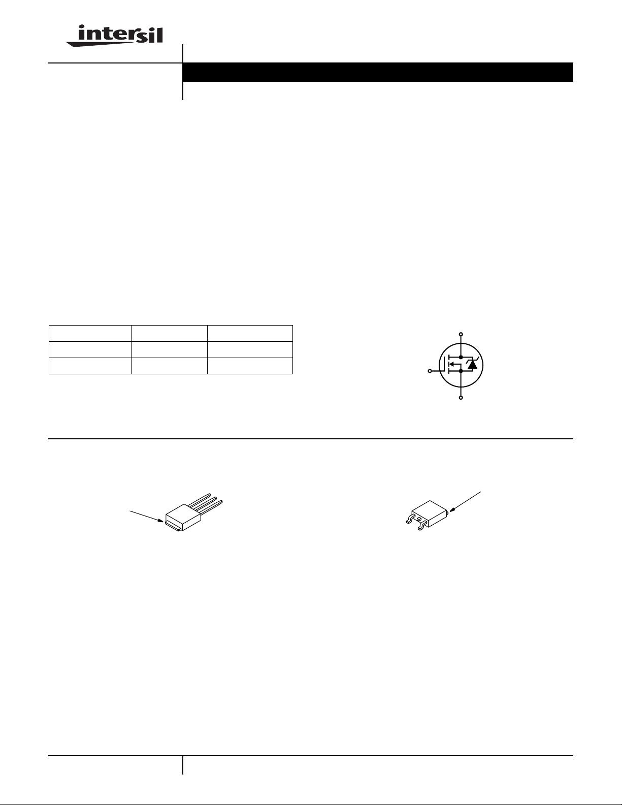
Symbol
D
G
S
Packaging
(FLANGE)
DRAIN
JEDEC TO-251AA JEDEC TO-252AA
SOURCE
DRAIN
GATE
GATE
SOURCE
DRAIN
(FLANGE)
1
CAUTION: These devices are sensitive to electrostatic discharge; follow proper ESD Handling Procedures.
PSPICE® is a registered trademark of MicroSim Corporation.
http://www.intersil.com or 407-727-9207
| Copyright © Intersil Corporation 1999
Page 2
RFD7N10LE, RFD7N10LESM
Absolute Maximum Ratings T
= 25oC, Unless Otherwise Specified
C
RFD7N10LE,
RFD7N10LESM UNITS
Drain to Source Voltage. . . . . . . . . . . . . . . . . . . . . . . . . . . . . . . . . . . . . . . . . . . .V
Drain to Gate Voltage. . . . . . . . . . . . . . . . . . . . . . . . . . . . . . . . . . . . . . . . . . . . . V
Gate to Source Voltage . . . . . . . . . . . . . . . . . . . . . . . . . . . . . . . . . . . . . . . . . . . . .V
DSS
DGR
GS
100 V
100 V
+10, -8 V
Drain Current
Continuous. . . . . . . . . . . . . . . . . . . . . . . . . . . . . . . . . . . . . . . . . . . . . . . . . . . . . . .I
Pulsed Drain Current . . . . . . . . . . . . . . . . . . . . . . . . . . . . . . . . . . . . . . . . . . . . . I
Pulsed Avalanche Rating. . . . . . . . . . . . . . . . . . . . . . . . . . . . . . . . . . . . . . . . . . . . E
Power Dissipation . . . . . . . . . . . . . . . . . . . . . . . . . . . . . . . . . . . . . . . . . . . . . . . . . .P
DM
AS
D
Refer to Peak Current Curve
Refer to UIS Curve
D
Derate Above 25oC . . . . . . . . . . . . . . . . . . . . . . . . . . . . . . . . . . . . . . . . . . . . . . . . .
Operating and Storage Temperature . . . . . . . . . . . . . . . . . . . . . . . . . . . . . . . TJ, T
STG
Maximum Temperature for Soldering
Leads at 0.063in (1.6mm) from Case for 10s. . . . . . . . . . . . . . . . . . . . . . . . . . . . T
Package Body for 10s, See Techbrief 334 . . . . . . . . . . . . . . . . . . . . . . . . . . . . .T
CAUTION: Stresses above those listed in “Absolute Maximum Ratings” may cause permanent damage to the device. This is a stress only rating and operation of the
device at these or any other conditions above those indicated in the operational sections of this specification is not implied.
L
pkg
7
47
0.318
-55 to 175
300
260
A
W
W/oC
o
C
o
C
o
C
NOTE:
1. TJ= 25oC to 150oC.
Electrical Specifications T
= 25oC, Unless Otherwise Specified
C
PARAMETER SYMBOL TEST CONDITIONS MIN TYP MAX UNITS
Drain to Source Breakdown Voltage BV
Gate Threshold Voltage V
Zero Gate Voltage Drain Current I
DSS
GS(TH)
DSS
ID = 250µA, VGS = 0V 100 - - V
VGS = VDS, ID = 250µA1-3V
VDS = 95V, VGS = 0V - - 1 µA
VDS = 90V, VGS = 0V, TC = 150oC - - 250 µA
Gate to Source Leakage Current I
On Resistance r
DS(ON)ID
Turn-On Time t
Turn-On Delay Time t
d(ON)
Rise Time t
Turn-Off Delay Time t
d(OFF)
Fall Time t
Turn-Off Time t
Total Gate Charge Q
g(TOT)
Gate Charge at 5V Q
Threshold Gate Charge Q
Input Capacitance C
Output Capacitance C
Reverse Transfer Capacitance C
Thermal Resistance Junction to Case R
Thermal Resistance Junction to Ambient R
GSS
ON
r
f
OFF
g(5)
g(TH)
ISS
OSS
RSS
θJC
θJA
VGS = +10, -8V - - 10 µA
= 7A, VGS = 5V - - 0.300 Ω
VDD = 50V, ID = 7A
RL = 7.1Ω, VGS = 5V
RGS = 2.5Ω
- - 110 ns
-10- ns
-65- ns
-23- ns
-18- ns
- - 60 ns
VGS = 0 to 10V VDD = 80V
VGS = 0 to 5V - 67 80 nC
ID = 7A,
RL = 11.4Ω
- 125 150 nC
VGS = 0 to 1V - 3.7 4.5 nC
VDS = 25V, VGS = 0V
f = 1MHz
- 360 - pF
-70- pF
-20- pF
- - 3.15
TO-251 and TO-252 Package - - 100
o
C/W
o
C/W
Source to Drain Diode Specifications
PARAMETER SYMBOL TEST CONDITIONS MIN TYP MAX UNITS
Source to Drain Diode Voltage V
Reverse Recovery Time t
2
SD
rr
ISD = 7A - - 1.5 V
ISD = 7A, dISD/dt = 100A/µs - - 130 ns
Page 3
RFD7N10LE, RFD7N10LESM
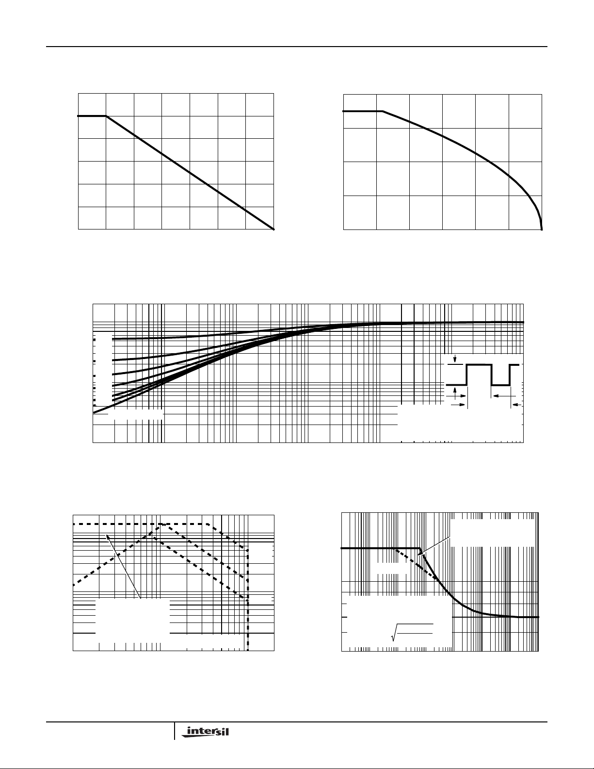
Typical Performance Curves Unless Otherwise Specified
1.2
1.0
0.8
0.6
0.4
0.2
POWER DISSIPATION MULTIPLIER
0
0
25 50 75 100
125
150
TC, CASE TEMPERATURE (oC)
FIGURE 1. NORMALIZED POWER DISSIPATION vs CASE
TEMPERATURE
1
0.5
0.2
0.1
0.1
0.05
NORMALIZED
0.02
θJC,
0.01
Z
THERMAL IMPEDANCE
0.01
-5
10
SINGLE PULSE
-4
10
-3
10
t, RECTANGULAR PULSE DURATION (s)
8
6
4
, DRAIN CURRENT (A)
2
D
I
1750
0
25 50 75 100
125 150
175
TC, CASE TEMPERATURE (oC)
FIGURE 2. MAXIMUM CONTINUOUS DRAIN CURRENT vs
CASE TEMPERATURE
P
DM
t
1
t
θJC
2
X R
θJC
2
+ T
C
1
10
NOTES:
DUTY FACTOR: D = t1/t
PEAK TJ = PDM X Z
-2
10
-1
10
0
10
FIGURE 3. NORMALIZED MAXIMUM TRANSIENT THERMAL IMPEDANCE
20
14
10
1
, DRAIN CURRENT (A)
D
I
OPERATION IN THIS
AREA MAY BE
LIMITED BY r
DS(ON)
TC = 25oC
0.1
J
V
DSS
MAX = 100V
T
= MAX RATED
1 10 200
VDS, DRAIN TO SOURCE VOLTAGE (V)
100µs
1ms
10ms
20
14
VGS = 5V
10
, PEAK CURRENT (A)
I
FOR TEMPERATURES
ABOVE 25
CURRENT AS FOLLOWS:
DM
I = I
5
-3
10
10
25
-2
o
C DERATE PEAK
175 - T
(
10
C
150
-1
10
t, PULSE WIDTH (ms)
TRANSCONDUCTANCE
MAY LIMIT CURRENT
IN THIS REGION
)
1
0
10
10
FIGURE 4. FORWARD BIAS SAFE OPERATING AREA FIGURE 5. PEAK CURRENT CAPABILITY
3
2
10
4
3
10
Page 4

RFD7N10LE, RFD7N10LESM
Typical Performance Curves Unless Otherwise Specified (Continued)
20
14
10
, AVALANCHE CURRENT (A)
If R = 0
tAV = (L)(IAS)/(1.3*RATED BV
AS
I
If R ≠ 0
t
= (L/R)ln[(IAS*R)/(1.3*RATED BV
AV
1
0.001 0.01 0.1 1
tAV, TIME IN AVALANCHE (ms)
STARTING T
STARTING TJ = 150oC
- VDD)
DSS
- VDD) +1]
DSS
= 25oC
J
15
10
5
, DRAIN CURRENT (A)
D
I
0
0 1.5
VDS, DRAIN TO SOURCE VOLTAGE (V)
VGS = 10V
PULSE DURATION = 80µs
DUTY CYCLE = 0.5% MAX
T
= 25oC
C
3.0
VGS = 5V
4.5
FIGURE 6. UNCLAMPED INDUCTIVE SWITCHING FIGURE 7. SATURATION CHARACTERISTICS
15
VDD = 15V
PULSE DURATION = 80µs
DUTY CYCLE = 0.5% MAX
10
-55oC
25oC
175oC
3.0
PULSE DURATION = 80µs
DUTY CYCLE = 0.5% MAX
V
= 5V, ID = 7A
GS
2.5
2.0
1.5
= 4.5V
V
GS
V
= 4V
GS
= 3V
V
GS
6.0 7.5
5
, DRAIN CURRENT (A)
D
I
0
0 345671
FIGURE 8. TRANSFER CHARACTERISTICS FIGURE 9. NORMALIZED DRAIN TOSOURCE ON
2.0
VGS= VDS,ID = 250µA
1.5
1.0
NORMALIZED GATE
0.5
THRESHOLD VOLTAGE
0
-80 -40
T
2
V
, GATE TO SOURCE VOLTAGE (V)
GS
04080
, JUNCTION TEMPERATURE (oC)
J
160
120 200
1.0
0.5
NORMALIZED ON RESISTANCE
0
-80 -40
04080
, JUNCTION TEMPERATURE (oC)
T
J
120
RESISTANCE vs JUNCTION TEMPERATURE
2.0
ID = 250µA
1.5
1.0
0.5
BREAKDOWN VOLTAGE
NORMALIZED DRAIN TO SOURCE
0
-80 -40 0 40 80 120 160 200
TJ, JUNCTION TEMPERATURE (oC)
160
200
FIGURE 10. NORMALIZED GATE THRESHOLD VOLTAGE vs
JUNCTION TEMPERATURE
4
FIGURE 11. NORMALIZED DRAIN TO SOURCE BREAKDOWN
VOLTAGE vs JUNCTION TEMPERATURE
Page 5

RFD7N10LE, RFD7N10LESM
Typical Performance Curves Unless Otherwise Specified (Continued)
600
400
C
ISS
VGS = 0V, f = 1MHz
C
= CGS + C
C
C
ISS
RSS
OSS
= C
≈ CDS + C
GD
GD
200
C, CAPACITANCE (pF)
0
0
510152025
C
C
OSS
RSS
VDS, DRAIN TO SOURCE VOLTAGE (V)
FIGURE 12. CAPACITANCE vs DRAIN TO SOURCE VOLTAGE
Test Circuits and Waveforms
V
DS
L
VARY t
TO OBTAIN
P
REQUIRED PEAK I
V
GS
AS
R
G
DUT
+
-
V
GD
DD
100
75
50
25
, DRAIN TO SOURCE VOLTAGE (V)
DS
V
0
VDD = BV
I
GREF()
--------------------- -
20
I
G ACT()
DSS
0.75 BV
0.50 BV
0.25 BV
0.75 BV
DSS
0.50 BV
DSS
0.25 BV
DSS
RL = 14.28Ω
I
= 0.24mA
G(REF)
VGS = 5V
t, TIME (µs)
VDD = BV
DSS
DSS
DSS
I
GREF()
--------------------- -
80
I
G ACT()
DSS
5.00
3.75
2.50
1.25
0
NOTE: Refer to Intersil Application Notes AN7254 and AN7260.
FIGURE 13. NORMALIZED SWITCHING WAVEFORMSFOR
CONSTANT GATE CURRENT
BV
DSS
t
P
I
AS
V
DS
V
DD
, GATE TO SOURCE VOLTAGE (V)
GS
V
0V
P
I
AS
0.01Ω
0
t
AV
t
FIGURE 14. UNCLAMPED ENERGY TEST CIRCUIT FIGURE 15. UNCLAMPED ENERGY WAVEFORMS
t
ON
t
DS
GS
10%
d(ON)
90%
50%
t
10%
r
PULSE WIDTH
V
DS
V
R
DUT
L
+
V
DD
-
0
V
0
V
GS
R
GS
V
GS
t
d(OFF)
90%
t
FIGURE 16. RESISTIVE SWITCHING TEST CIRCUIT FIGURE 17. RESISTIVE SWITCHING WAVEFORMS
OFF
50%
t
f
10%
90%
5
Page 6

PSPICE Electrical Model
SUBCKT RFD7N10LE 2 1 3; rev 6/2/93
CA 12 8 7.5e-10
CB 15 14 7.6e-10
CIN 6 8 4.03e-10
RFD7N10LE, RFD7N10LESM
DBODY 7 5 DBODYMOD
DBREAK 5 11 DBREAKMOD
DPLCAP 10 5 DPLCAPMOD
EBREAK 11 7 17 18 116.7
EDS 14 8 5 8 1
EGS 13 8 6 8 1
ESG 6 10 6 8 1
EVTHRES 6 21 19 8 1
EVTEMP 20 6 18 22 1
IT 8 17 1
LDRAIN 2 5 1e-9
LGATE 1 9 3.7e-9
LSOURCE 3 7 3.4e-9
GATE
1
MMED 16 6 8 8 MMEDMOD
MSTRO 16 6 8 8 MSTROMOD
MWEAK 16 21 8 8 MWEAKMOD
RBREAK 17 18 RBREAKMOD 1
RDRAIN 50 16 RDRAINMOD 9.4e-2
RGATE 9 20 3.3
RLDRAIN 2 5 10
RLGATE 1 9 37
RLSOURCE 3 7 34
RSLC1 5 51 RSLCMOD 1e-6
RSLC2 5 50 1e3
RSOURCE 8 7 RSOURCEMOD 1.3e-2
RVTHRES 22 8 RVTHRESMOD 1
RVTEMP 18 19 RVTEMPMOD 1
S1A 6 12 13 8 S1AMOD
S1B 13 12 13 8 S1BMOD
S2A 6 15 14 13 S2AMOD
LGATE
RLGATE
RGATE
9
CA
ESG
EVTEMP
+
18
22
20
S1A
12
13
8
S1B
EGS EDS
-
+
-
6
8
13
10
RSLC2
6
14
13
+
+
6
8
-
-
DPLCAP
EVTHRES
+
19
8
S2A
S2B
15
CIN
CB
-
+
51
5
8
-
5
RSLC1
51
+
5
-
50
RDRAIN
21
MSTRO
14
ESLC
16
8
MMED
DBREAK
11
EBREAK
MWEAK
RSOURCE
RBREAK
17 18
IT
8
RVTHRES
+
17
18
-
S2B 13 15 14 13 S2BMOD
VBAT 22 19 DC 1
ESLC 51 50 VALUE={(V(5,51)/ABS(V(5,51)))*(PWR(V(5,51)/(1e-6*17.3),3.5))}
.MODEL DBODYMOD D (IS = 1.2e-12 RS = 1.2e-2 TRS1 = 1.2e-3 TRS2 = 1.03e-6 CJO = 6.7e-10 TT = 6.9e-8 M = 0.77)
.MODEL DBREAKMOD D (RS = 9.9e-1 TRS1 = 1e-3 TRS2 = -2e-5)
.MODEL DPLCAPMOD D (CJO = 4.3e-10 IS = 1e-30 M = 0.9 N = 10)
.MODEL MMEDMOD NMOS (VTO = 1.88 KP = 5 IS = 1e-30 N = 10 TOX = 1 L = 1u W = 1u RG = 3.3)
.MODEL MSTROMOD NMOS (VTO = 2.13 KP = 12.4 IS = 1e-30 N = 10 TOX = 1 L = 1u W = 1u)
.MODEL MWEAKMOD NMOS (VTO = 1.59 KP = 0.12 IS = 1e-30 N = 10 TOX = 1 L = 1u W = 1u RG = 33 RS = 0.1)
.MODEL RBREAKMOD RES (TC1 = 1.05e-3 TC2 = -5e-7)
.MODEL RDRAINMOD RES (TC1 = 8.1e-3 TC2 = 2.4e-5)
.MODEL RSLCMOD RES (TC1 = 3e-3 TC2 = 2e-6)
.MODEL RSOURCEMOD RES (TC1 = 1e-3 TC2 = 1e-6)
.MODEL RVTHRESMOD RES (TC1 = -1.5e-3 TC2 = -4.3e-6)
.MODEL RVTEMPMOD RES (TC1 = -1.6e-3 TC2 = 1.5e-6)
.MODEL S1AMOD VSWITCH (RON = 1e-5 ROFF = 0.1 VON = -4.5 VOFF= -2.5)
.MODEL S1BMOD VSWITCH (RON = 1e-5 ROFF = 0.1 VON = -2.5 VOFF= -4.5)
.MODEL S2AMOD VSWITCH (RON = 1e-5 ROFF = 0.1 VON = -0.3 VOFF= 0.2)
.MODEL S2BMOD VSWITCH (RON = 1e-5 ROFF = 0.1 VON = 0.2 VOFF= -0.3)
.ENDS
7
RVTEMP
19
-
+
22
LDRAIN
RLDRAIN
DBODY
LSOURCE
RLSOURCE
VBAT
DRAIN
2
SOURCE
3
NOTE: Forfurther discussion ofthePSPICEmodelconsultANewPSPICE Sub-Circuit for the Power MOSFET Featuring Global Temperature Options;
IEEE Power Electronics Specialist Conference Records 1991.
6
Page 7

RFD7N10LE, RFD7N10LESM
All Intersil semiconductor products are manufactured, assembled and tested under ISO9000 quality systems certification.
Intersil semiconductor products are sold by description only. Intersil Corporation reserves the right to make changes in circuit design and/or specifications at any time without notice. Accordingly, the reader is cautioned to verify that data sheets are current before placing orders. Information furnished by Intersil is believed to be accurate and
reliable. However,no responsibility is assumed by Intersil or its subsidiaries for its use; nor for any infringements of patents or other rights of third parties which may result
from its use. No license is granted by implication or otherwise under any patent or patent rights of Intersil or its subsidiaries.
For information regarding Intersil Corporation and its products, see web site http://www.intersil.com
Sales Office Headquarters
NORTH AMERICA
Intersil Corporation
P. O. Box 883, Mail Stop 53-204
Melbourne, FL 32902
TEL: (407) 724-7000
FAX: (407) 724-7240
7
EUROPE
Intersil SA
Mercure Center
100, Rue de la Fusee
1130 Brussels, Belgium
TEL: (32) 2.724.2111
FAX: (32) 2.724.22.05
ASIA
Intersil (Taiwan) Ltd.
7F-6, No. 101 Fu Hsing North Road
Taipei, Taiwan
Republic of China
TEL: (886) 2 2716 9310
FAX: (886) 2 2715 3029
 Loading...