

Page 1
RFD3N08L, RFD3N08LSM
Data Sheet July 1999
3A, 80V, 0.800 Ohm, Logic Level,
N-Channel Power MOSFETs
The RFD3N08L and RFD3N08LSM are N-Channel
enhancement mode silicon gate powerfieldeffecttransistors
specifically designed for use with logic level (5V) driving
sources in applications such as programmable controllers,
automotive switching, and solenoid drivers. This
performance is accomplished through a special gate oxide
design which provides full rated conductance at gate biases
in the 3V to 5V range, thereby facilitating true on-off power
control directly from logic circuit supply voltages.
Formerly developmental type TA09922.
Ordering Information
PART NUMBER PACKAGE BRAND
RFD3N08L TO-251AA F3N08L
RFD3N08LSM TO-252AA F3N08L
NOTE: When ordering,include the entirepartnumber.Add the suffix9A
to obtain the TO-252AA variant in tape and reel, i.e. RFD3N08LSM9A
File Number
Features
• 3A, 80V
DS(ON)
= 0.800Ω
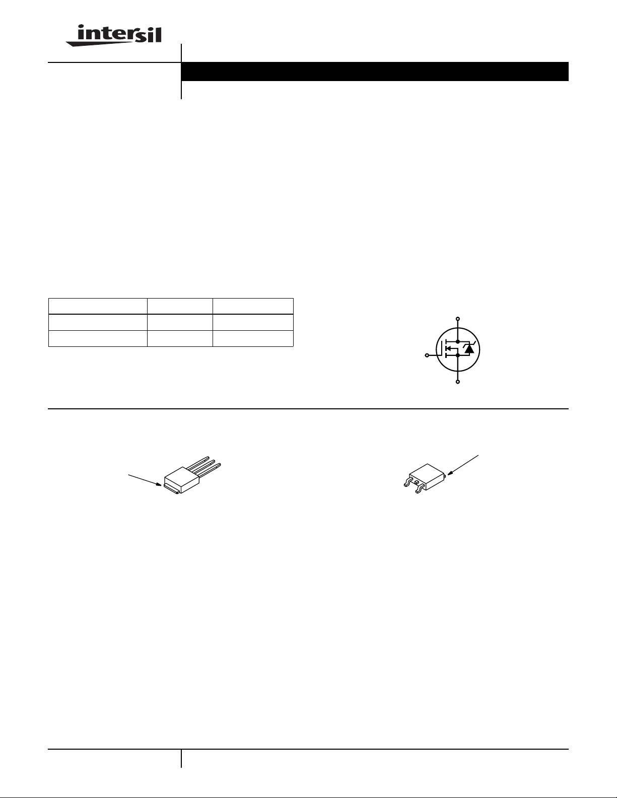
®
Model
•r
• Temperature Compensating PSPICE
• On Resistance vs Gate Drive Voltage Curves
• Peak Current vs Pulse Width Curve
• UIS Rating Curve
o
C Operating Temperature
• 175
• Related Literature
- TB334 “Guidelines for Soldering Surface Mount
Components to PC Boards”
Symbol
D
G
S
2836.4
Packaging
(FLANGE)
DRAIN
JEDEC TO-251AA JEDEC TO-252AA
SOURCE
DRAIN
GATE
GATE
SOURCE
DRAIN
(FLANGE)
6-26
CAUTION: These devices are sensitive to electrostatic discharge; follow proper ESD Handling Procedures.
PSPICE® is a registered trademark of MicroSim Corporation.
http://www.intersil.com or 407-727-9207
| Copyright © Intersil Corporation 1999
Page 2
RFD3N08L, RFD3N08LSM
Absolute Maximum Ratings T
= 25oC, Unless Otherwise Specified
C
RFD3N08L,
RFD3N08LSM UNITS
Drain to Source Voltage (Note 1). . . . . . . . . . . . . . . . . . . . . . . . . . . . . . . . . . . . . . . . V
Drain to Gate Voltage (RGS = 20KΩ) (Note 1). . . . . . . . . . . . . . . . . . . . . . . . . . . . . V
Gate to Source Voltage . . . . . . . . . . . . . . . . . . . . . . . . . . . . . . . . . . . . . . . . . . . . . . . V
Continuous Drain Current . . . . . . . . . . . . . . . . . . . . . . . . . . . . . . . . . . . . . . . . . . . . . . . I
Pulsed Drain Current (Figures 3, 5) (Note 3) . . . . . . . . . . . . . . . . . . . . . . . . . . . . . . I
Maximum Power Dissipation . . . . . . . . . . . . . . . . . . . . . . . . . . . . . . . . . . . . . . . . . . . . .P
DS
DGR
GS
DM
D
Refer to Peak Current Curve
D
Derate Above 25oC . . . . . . . . . . . . . . . . . . . . . . . . . . . . . . . . . . . . . . . . . . . . . . . . . . . .
Pulsed Avalanche Energy Rating (Figure 6) (Note 4) . . . . . . . . . . . . . . . . . . . . . . . . .E
Operating and Storage Temperature Range . . . . . . . . . . . . . . . . . . . . . . . . . . . .TJ, T
AS
STG
Maximum Temperature for Soldering
Leads at 0.063in (1.6mm) from Case for 10s. . . . . . . . . . . . . . . . . . . . . . . . . . . . . . . T
Package Body for 10s, See Techbrief 334 . . . . . . . . . . . . . . . . . . . . . . . . . . . . . . . T
CAUTION: Stresses above those listed in “Absolute Maximum Ratings” may cause permanent damage to the device. This is a stress only rating and operationofthe
device at these or any other conditions above those indicated in the operational sections of this specification is not implied.
L
pkg
80 V
80 V
±10 V
3
30
0.2
Refer to UIS Curve
-55 to 175
300
260
A
W
W/oC
o
C
o
C
o
C
NOTE:
1. TJ= 25oC to 150oC.
Electrical Specifications T
= 25oC, Unless Otherwise Specified
C
PARAMETER SYMBOL TEST CONDITIONS MIN TYP MAX UNITS
Drain to Source Breakdown Voltage BV
Gate to Threshold Voltage V
Zero Gate Voltage Drain Current I
DSSID
GS(TH)VGS
DSS
= 250µA, VGS = 0V (Figure 12) 80 - - V
= VDS, ID = 250µA (Figure 11) 1 - 2.5 V
VDS = Rated BV
VDS = 0.8 x Rated BV
, VGS = 0V - - 25 µA
DSS
DSS
,
- - 250 µA
VGS = 0V 125oC
Gate to Source Leakage Current I
Drain to Source On Resistance (Note 2) r
DS(ON)ID
Turn-On Time t
Turn-On Delay Time t
d(ON)
Rise Time t
Turn-Off Delay Time t
d(OFF)
Fall Time t
Turn-Off Time t
Total Gate Charge Q
(OFF)
g(TOT)VGS
Gate Charge at 5V Q
Threshold Gate Charge Q
Input Capacitance C
Output Capacitance C
Reverse Transfer Characterisics C
Thermal Resistance, Junction to Case R
Thermal Resistance, Junction to Ambient R
GSS
(ON)
g(TH)VGS
OSS
RSS
VGS = ±10V - - ±100 nA
= 3A, VGS = 5V, (Figures 9, 10) - - 0.800 Ω
VDD = 40V, ID = 3A,
RL = 13.3Ω, VGS = 5V,
RG = 25Ω,
(Figures 13, 15, 18, 19)
r
- - 75 ns
-15 - ns
-45 - ns
-22 - ns
f
-15 - ns
- - 45 ns
= 0V to 10V VDD = 64V, ID = 3A,
I
= 0.1mA
VGS = 0V to 5V - 3.8 4.8 nC
g(5)
= 0V to 1V - 0.18 0.24 nC
VDS = 25V, VGS = 0V, f = 1MHz,
ISS
g(REF)
RL = 21.3Ω
(Figures 15, 20, 21)
(Figure 14)
- 6.8 8.5 nC
- - 125 pF
- - 55 pF
- - 15 pF
θJC
θJA
- - 5.0
- - 100
o
o
C/W
C/W
Source to Drain Diode Ratings and Specifications
PARAMETER SYMBOL TEST CONDITIONS MIN TYP MAX UNITS
Source to Drain Diode Voltage (Note 2) V
Reverse Recovery Time t
SDISD
rr
NOTES:
2. Pulsed: pulse duration = 300µs max, duty cycle = 2%.
3. Repetitive rating: pulse width limited by maximum junction temperature. See Transient Thermal Impedance curve (Figure 3).
4. Refer to Intersil Application Notes AN9321 and AN9322.
6-27
= 3A - - 1.25 V
ISD = 3A, dISD/dt = 100A/µs--85ns
Page 3
RFD3N08L, RFD3N08LSM
Typical Performance Curves
Unless Otherwise Specified
1.2
1.0
0.8
0.6
0.4
0.2
POWER DISSIPATION MULTIPLIER
0
25 50 75 100
0
0
125
TC, CASE TEMPERATURE (oC)
FIGURE 1. NORMALIZED POWER DISSIPATIONvs CASE
TEMPERATURE
1
0.5
150
175
3.5
3.0
2.5
2.0
1.5
, DRAIN CURRENT (A)
1.0
D
I
0.5
0
25 50 75 100 125 150
TC, CASE TEMPERATURE (oC)
FIGURE 2. MAXIMUM CONTINUOUS DRAIN CURRENT vs
TEMPERATURE
175
0.2
0.1
0.1
0.05
0.02
, NORMALIZED TRANSIENT
θJC
Z
0.01
10
-5
SINGLE PULSE
10
-4
0.01
THERMAL IMPEDANCE
FIGURE 3. NORMALIZED MAXIMUM TRANSIENT THERMAL IMPEDANCE
20
10
1
, DRAIN CURRENT (A)
D
I
OPERATION IN THIS
AREA MAY BE
LIMITED BY r
0.1
1 10 100
DS(ON)
VDS, DRAIN TO SOURCE VOLTAGE (V)
V
MAX = 80V
DSS
TC = 25oC
= MAX RATED
T
J
-3
10
-2
10
t, RECTANGULAR PULSE DURATION (s)
30
100µs
10
1ms
10ms
100ms
DC
200
, PEAK CURRENT CAPABILITY (A)
DM
I
1
10
NOTES:
DUTY FACTOR: D = t
PEAK TJ = PDM x Z
-1
10
VGS = 10V
VGS = 5V
TRANSCONDUCTANCE
MAY LIMIT CURRENT
IN THIS REGION
-5
-4
10
10
P
DM
0
10
FOR TEMPERATURES
ABOVE 25oC DERATE PEAK
CURRENT AS FOLLOWS:
I = I
25
-3
-2
10
t, PULSE WIDTH (s)
t
t
1/t2
x R
θJC
175 - T
TC = 25oC
-1
10
1
2
150
θJC
+ T
C
1
10
C
0
10
1
10
FIGURE 4. FORWARD BIAS SAFE OPERATING AREA FIGURE 5. PEAK CURRENT CAPABILITY
6-28
Page 4

RFD3N08L, RFD3N08LSM
Typical Performance Curves
20
If R = 0
tAV = (L)(IAS)/(1.3*RATED BV
If R ≠ 0
10
tAV = (L/R)ln[(IAS*R)/(1.3*RATED BV
STARTING TJ = 150oC
, AVALANCHE CURRENT (A)
AS
I
1
0.001
0.01
tAV, TIME IN AVALANCHE (ms)
DSS
STARTING TJ = 25oC
Unless Otherwise Specified (Continued)
- VDD)
- VDD) +1]
DSS
0.1 1
NOTE: Refer to Intersil Application Notes AN9321 and AN9322.
FIGURE 6. UNCLAMPED INDUCTIVE SWITCHING CAPABILITY
10
PULSE DURATION = 80µs
DUTY CYCLE = 0.5% MAX
V
= 15V
DD
8
-55oC
10
VGS = 10V
8
6
4
, DRAIN CURRENT (A)
D
I
2
0
0246810
VDS, DRAIN TO SOURCE VOLTAGE (V)
PULSE DURATION = 80µs
DUTY CYCLE = 0.5% MAX
TC = 25oC
V
= 5V
GS
VGS = 4.5V
= 4V
V
GS
VGS = 3.5V
= 3V
V
GS
FIGURE 7. SATURATION CHARACTERISTICS
2.5
ID = 4A
2
ID = 3A
6
4
2
, DRAIN TO SOURCE CURRENT (A)
DS(ON)
I
0
0 3 4.5 6 7.51.5
VGS, GATE TO SOURCE VOLTAGE (V)
25oC
175oC
1.5
, ON-STATE RESISTANCE (Ω)
0.5
DS(ON)
r
ID = 1.5A
1
ID = 0.75A
PULSE DURATION = 80µs
DUTY CYCLE = 0.5% MAX
V
= 15V
0
2.5 3.5 4 4.5 5
32
V
, GATE TO SOURCE VOLTAGE (V)
GS
DD
FIGURE 8. TRANSFER CHARACTERISTICS FIGURE 9. DRAIN TO SOURCE ON RESISTANCE vs GATE
VOLTAGE AND DRAIN CURRENT
NORMALIZED GATE
2
VGS = VDS,ID = 250µA
1.5
1
0.5
THRESHOLD VOLTAGE
3
PULSE DURATION = 80µs
DUTY CYCLE = 0.5% MAX
2.5
V
= 5V, ID = 3A
GS
2
1.5
1
0.5
NORMALIZED ON RESISTANCE
0
-80 -40 0 40 80 120 200
TJ, JUNCTION TEMPERATURE (oC)
FIGURE 10. NORMALIZED DRAIN TOSOURCE ON
RESISTANCE vs JUNCTION TEMPERATURE
6-29
160
0
-80 -40 0 40 80 120 200
TJ, JUNCTION TEMPERATURE (oC)
160
FIGURE 11. NORMALIZED GATETHRESHOLD VOLTAGEvs
JUNCTION TEMPERATURE
Page 5

RFD3N08L, RFD3N08LSM
Typical Performance Curves
2.0
ID = 250µA
Unless Otherwise Specified (Continued)
1.5
1.0
0.5
BREAKDOWN VOLTAGE
NORMALIZED DRAIN TO SOURCE
0
-80 -40 0 40 80 120 160
T
, JUNCTION TEMPERATURE (oC)
J
FIGURE 12. NORMALIZED DRAIN TOSOURCE BREAKDOWN
VOLTAGE vs JUNCTION TEMPERATURE
180
C
150
120
ISS
C
OSS
90
60
C
C, CAPACITANCE (pF)
RSS
30
0
0 5 10 15 20 25
VDS, DRAIN TO SOURCE VOLTAGE (V)
VGS = 0V, f = 1MHz
= CGS + C
C
C
C
ISS
RSS
OSS
= C
≈ CDS + C
GD
GD
FIGURE 14. CAPACITANCE vs DRAIN TO SOURCE VOLTAGE
GD
200
100
VDD = 40V, ID = 3A, RL = 13.3Ω
t
r
80
60
t
t
d(OFF)
t
d(ON)
f
40
SWITCHING TIME (ns)
20
0
10
20 30 40 500
RGS, GATE TO SOURCE RESISTANCE (Ω)
FIGURE 13. SWITCHING TIME vs GATE RESISTANCE
80
60
40
20
, DRAIN TO SOURCE VOLTAGE (V)
DS
V
0
RL = 26.67Ω
I
G(REF)
V
PLATEAU VOLTAGES IN
DESCENDING ORDER:
V
DD
VDD = 0.75 BV
VDD = 0.50 BV
VDD = 0.25BV
I
G(REF)
20
I
G(ACT)
= 0.1mA
= 5V
GS
= BV
DSS
t, TIME (µs)
DSS
DSS
DSS
80
I
G(REF)
I
G(ACT)
5.00
3.75
2.50
1.25
0
NOTE: Refer to Intersil Application Notes AN7254 and AN7260.
FIGURE 15. NORMALIZED SWITCHING WAVEFORMS FOR
CONSTANT GATE CURRENT
, GATE TO SOURCE VOLTAGE (V)
GS
V
Test Circuits and Waveforms
V
DS
BV
DSS
L
VARY t
TO OBTAIN
P
REQUIRED PEAK I
V
GS
AS
R
G
+
V
DD
-
DUT
0V
P
I
AS
0.01Ω
0
t
FIGURE 16. UNCLAMPED ENERGY TEST CIRCUIT FIGURE 17. UNCLAMPED ENERGY WAVEFORMS
6-30
t
P
I
AS
t
AV
V
DS
V
DD
Page 6

RFD3N08L, RFD3N08LSM
Test Circuits and Waveforms
R
G
V
GS
FIGURE 18. SWITCHING TIME TEST CIRCUIT FIGURE 19. RESISTIVE SWITCHING WAVEFORMS
V
DS
V
GS
I
g(REF)
(Continued)
R
L
DUT
R
L
DUT
t
ON
t
d(ON)
t
V
DS
90%
+
V
DD
-
0
r
10%
t
d(OFF)
t
OFF
t
f
90%
10%
90%
V
GS
10%
0
V
DD
50%
PULSE WIDTH
Q
g(TOT)
V
DS
50%
VGS= 10V
+
V
DD
-
V
GS
Q
g(5)
VGS= 5V
VGS= 1V
0
Q
g(TH)
I
G(REF)
0
FIGURE 20. GATE CHARGE TEST CIRCUIT FIGURE 21. GATE CHARGE WAVEFORMS
6-31
Page 7

PSPICE Electrical Model
SUBCKT RFD3N08L 2 1 3 ; rev 5/10/95
CA 12 8 4.10e-10
CB 15 14 3.25e-10
CIN 6 8 1.10e-10
DBODY 7 5 DBDMOD
DBREAK 5 11 DBREAKMOD
DPLCAP 10 5 DPLCAPMOD
EBREAK 11 7 17 18 93.57
EDS 14 8 5 8 1
EGS 13 8 6 8 1
ESG 6 10 6 8 1
EVTHRESH 6 21 19 8 1
EZTEMPCO 20 6 18 22 1
IT 8 17 1
LDRAIN 2 5 1e-9
LGATE 1 9 5.8e-9
LSOURCE 3 7 5.8e-9
MOS1 16 6 8 8 MSTRONG M = 0.80
MOS2 16 21 8 8 MWEAK M = 0.20
RBREAK 17 18 RBREAKMOD 1
RDRAIN 50 16 RDRAINMOD 174.2e-3
RGATE 9 20 24.9
RIN 6 8 1e9
RLDRAIN 2 5 10
RLGATE 1 9 58
RLSOURCE 3 7 58
RSCL1 5 51 RSCLMOD 1e-6
RSCL2 5 50 1e3
RSOURCE 8 7 RSOURCEMOD 200.2e-3
RTHRESH 22 8 RTHRESHMOD 1
RZTEMPCO 18 19 RZTEMPCOMOD 1
S1A 6 12 13 8 S1AMOD
S1B 13 12 13 8 S1BMOD
S2A 6 15 14 13 S2AMOD
S2B 13 15 14 13 S2BMOD
LGATE
GATE
1
RLGATE
RFD3N08L, RFD3N08LSM
9
RGATE
10
ESG
EZTEMPCO
20
+
18
22
S1A
12
13814
S1B
CA
EGS
6
8
+
RIN
+
DPLCAP
RSCL2
EVTHRESH
+
6
S2A
15
13
S2B
13
6
EDS
8
19
8
CIN
CB
16
5
51
+
5
8
RSCL1
51
+
5
ESCL
50
RDRAIN
21
MOS1
14
8
DBREAK
11
EBREAK
MOS2
RSOURCE
17
+
17
18
7
RLSOURCE
RBREAK
RZTEMPCO
IT
RTHRESH
LDRAIN
RLDRAIN
DBODY
LSOURCE
DRAIN
2
3
SOURCE
18
19
VBAT
+
22
VBAT 22 19 DC 1
ESCL 51 50 VALUE = {(V(5,51)/ABS(V(5,51)))*(PWR(V(5,51)/(1e-6*10),6))}
.MODEL DBDMOD D (IS = 9.90e-14 RS = 6.00e-2 TRS1 = 1.42e-3 TRS2 = -3.58e-6 CJO = 1.40e-10 TT = 5.75e-8 M = 0.4)
.MODEL DBREAKMOD D (RS = 2.32 TRS1 = 1.03e-3 TRS2 = -6.17e-11)
.MODEL DPLCAPMOD D (CJO = 1.13e-10 IS = 1e-30 N = 10 M=0.6)
.MODEL MSTRONG NMOS (VTO = 1.773 KP = 1.70 IS = 1e-30 N = 10 TOX = 1L = 1u W = 1u)
.MODEL MWEAK NMOS (VTO = 1.496 KP = 2.09 IS = 1e-30 N = 10 TOX = 1L = 1u W = 1u)
.MODEL RBREAKMOD RES (TC1 = 8.19e-4 TC2 = 5.9e-7)
.MODEL RDRAINMOD RES (TC1 = 1.55e-2 TC2 = 8.58e-5)
.MODEL RDSOURCEMOD RES (TC1 = 0 TC2 = 0)
.MODEL RSCLMOD RES (TC1 = 0 TC2 = 0)
.MODEL RTHRESHMOD RES (TC1 = -5.0e-4 TC2 = -6.0e-6)
.MODEL RZTEMPCOMOD RES (TC1 = -1.19e-3 TC2 = 1.12e-6)
.MODEL S1AMOD VSWITCH (RON = 1e-5 ROFF = 0.1 VON = -5.2 VOFF= -3.2)
.MODEL S1BMOD VSWITCH (RON = 1e-5 ROFF = 0.1 VON = -3.2 VOFF= -5.2)
.MODEL S2AMOD VSWITCH (RON = 1e-5 ROFF = 0.1 VON = -0.60 VOFF= 4.4)
.MODEL S2BMOD VSWITCH (RON = 1e-5 ROFF = 0.1 VON = 4.4 VOFF= -0.60)
.ENDS
NOTE:
1. Forfurther discussionof the PSPICE model, consultA New PSPICE Sub-circuit for the Power MOSFET Featuring Global Temperature Options; IEEE
Power Electronics Specialist Conference Records, 1991.
6-32
Page 8

RFD3N08L, RFD3N08LSM
All Intersil semiconductor products are manufactured, assembled and tested under ISO9000 quality systems certification.
Intersil semiconductor products are sold by description only. Intersil Corporation reserves the right to make changes in circuit design and/or specifications at any time without notice. Accordingly, the reader is cautioned to verify that data sheets are current before placing orders. Information furnished by Intersil is believedto be accurate and
reliable. However, no responsibility is assumed by Intersil or its subsidiaries for its use; nor for any infringements of patents or other rights of third parties which may result
from its use. No license is granted by implication or otherwise under any patent or patent rights of Intersil or its subsidiaries.
For information regarding Intersil Corporation and its products, see web site http://www.intersil.com
Sales Office Headquarters
NORTH AMERICA
Intersil Corporation
P. O. Box 883, Mail Stop 53-204
Melbourne, FL 32902
TEL: (407) 724-7000
FAX: (407) 724-7240
6-33
EUROPE
Intersil SA
Mercure Center
100, Rue de la Fusee
1130 Brussels, Belgium
TEL: (32) 2.724.2111
FAX: (32) 2.724.22.05
ASIA
Intersil (Taiwan) Ltd.
7F-6, No. 101 Fu Hsing North Road
Taipei, Taiwan
Republic of China
TEL: (886) 2 2716 9310
FAX: (886) 2 2715 3029
 Loading...