

Page 1
CLC420
High-Speed, Voltage Feedback Op Amp
General Description
The CLC420 is an operational amplifier designed for applications requiring matched inputs, integration or transimpedance amplification. Utilizing voltage feedback architecture,
the CLC420 offers a 300MHz bandwidth, a 1100V/µs slew
rate and a 4mA supply current (power consumption of
40mW,
±
5V supplies).
Applications such as differential amplifiers will benefit from
70dB common mode rejection ratio and an input offset current of 0.2µA. With its unity-gain stability, 2pA/
current
noise and 3µA of input bias current, the CLC420 is designed
to meet the needs of filter applications and log amplifiers.
The low input offset current and current noise, combined
with a settling time of18ns to 0.01%make the CLC420 ideal
for D/A converters, pin diode receivers and photo multipliers
amplifiers. All applications will find 70dB power supply rejection ratio attractive.
Features
n 300MHz small signal bandwidth
n 1100V/µs slew rate
n Unity-gain stability
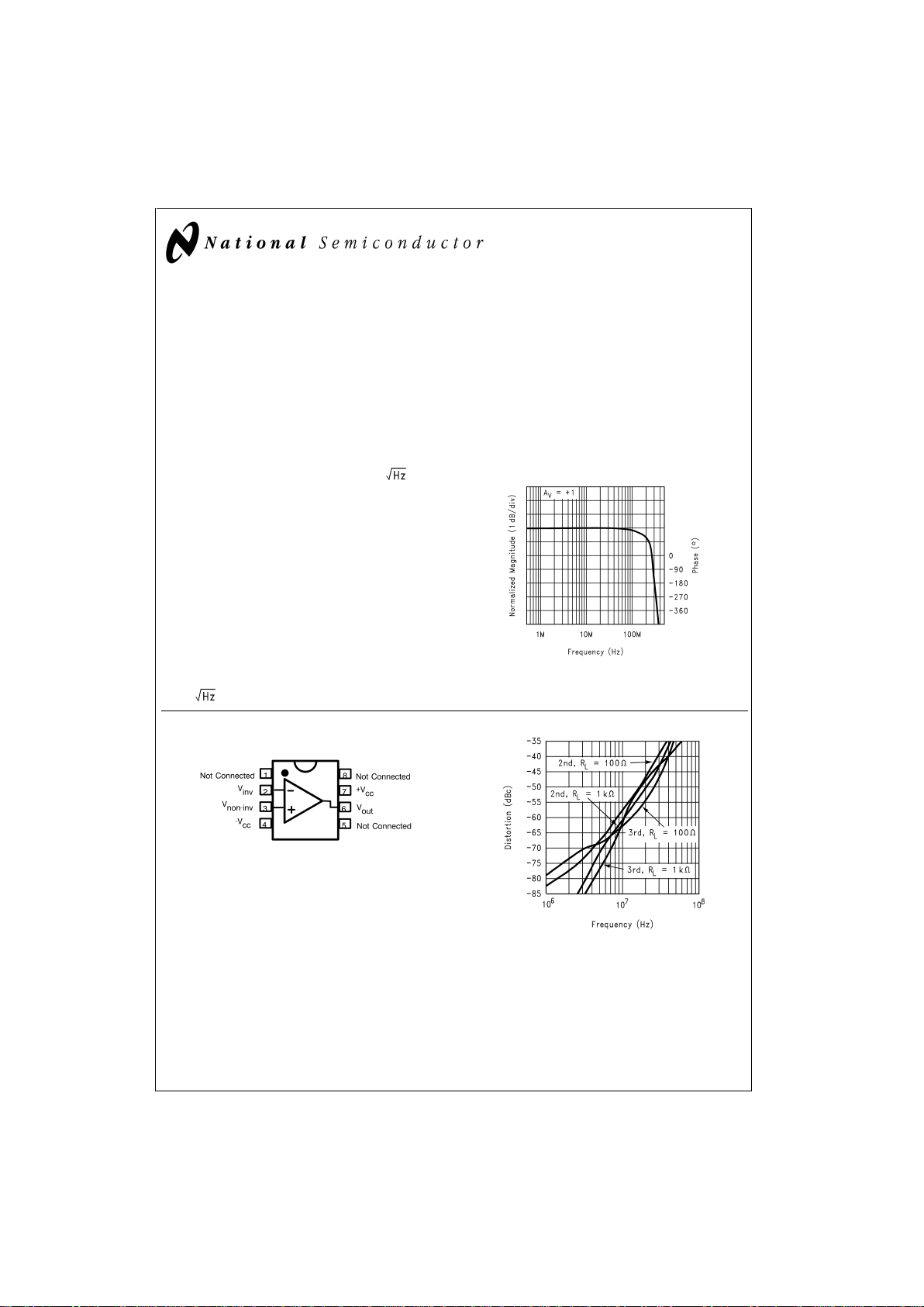
n Low distortion, -60dBc at 20MHz
n 0.01%settling in 18ns
n 0.2µA input offset current
n 2pA
current noise
Applications
n Active filters/integrators
n Differential amplifiers
n Pin diode receivers
n Log amplifiers
n D/A converters
n Photo multiplier amplifiers
Connection Diagram
Non-Inverting Frequency Response
DS012752-19
DS012752-18
Pinout
DIP & SOIC
DS012752-20
2nd and 3rd Harmonic Distortion
September 1999
CLC420 High-Speed, Voltage Feedback Op Amp
© 1999 National Semiconductor Corporation DS012752 www.national.com
Page 2

Ordering Information
Package Temperature Range
Industrial
Packaging
Marking
NSC
Drawing
8-pin plastic DIP −40˚C to +85˚C CLC420AJP N08E
8-pin plastic SOIC −40˚C to +85˚C CLC420AJE
CLC420AJE-TR13
M08A
CLC420
www.national.com 2
Page 3
Absolute Maximum Ratings (Note 1)
If Military/Aerospace specified devices are required,
please contact the National Semiconductor Sales Office/
Distributors for availability and specifications.
Supply Voltage (V
CC
)
±
7V
I
OUT
(is short circuit protected to ground,
but maximum reliability will be
maintained if I
OUT
does not exceed
70mA, except A8D, B8D which should
not exceed 35mA over the military
temperature range)..
Common Mode Input Voltage
±
V
CC
Differential Input Voltage 10V
Junction Temperature +150˚C
Operating Temperature Range
AJ: −40˚C to +85˚C
Storage Temperature Range −65˚C to +150˚C
Lead Solder Duration (+300˚C) 10 sec
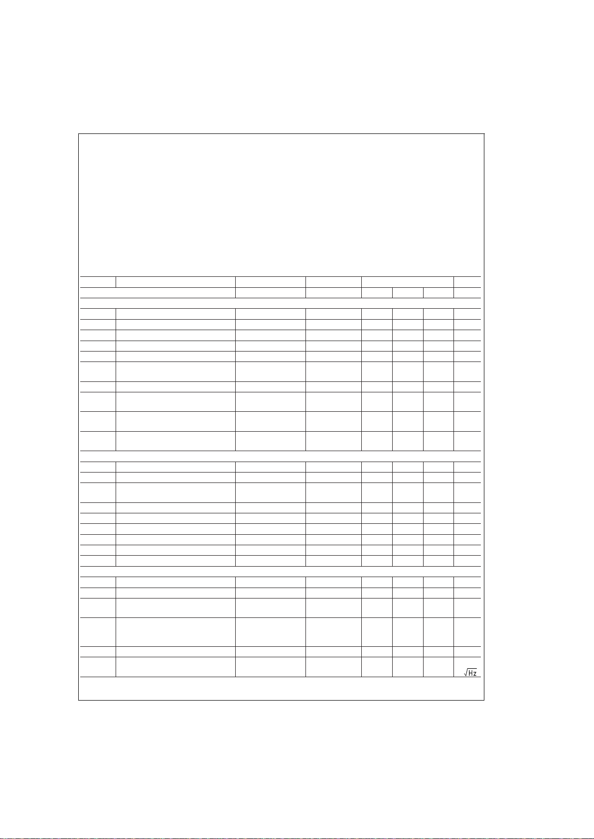
Electrical Characteristics
A
V
=
+1, V
CC
=
±
5V, R
L
=
100Ω,R
f
=
0Ω; unless specified
Symbol Parameter Conditions Typ Max/Min (Note 2) Units
Ambient Temperature CLC420AJ +25˚C −40˚C +25˚C +85˚
Frequency Domain Response
SSBW -3dB bandwidth V
OUT
<
0..4V
PP
300
>
200>200>130 MHz
LSBW V
OUT
<
5V
PP
40
>
20
>
25
>
20 MHz
SSBWI A
v
=
−1, R
f
=
500Ω V
OUT
<
0.4V
PP
100
>
65
>
65
>
45 MHz
LSBWI A
v
=
−1, R
f
=
500Ω V
OUT
<
5V
PP
60
>
30
>
35
>
30 MHz
gain flatness V
OUT
<
0.4V
PP
GFPL peaking 0.1MHz to
100MHz
0
<
1
<
0.6
<
0.6 dB
GFPH peaking
>
100MHz 0
<
5
<
3
<
3dB
GFR rolloff 0.1MHz to
100MHz
0.2
<
1
<
1
<
2dB
GFRI rolloff, A
v
=
−1, R
f
=
500Ω 0.1MHz to
30MHz
0.2
<
1.4
<
1.4
<
1.6 dB
LPD linear phase deviation 0.1MHz to
100MHz
0.9
<
1.8
<
1.8
<
2.5 ˚
Time Domain Response
TRS rise and fall time 0.4V step 1.2
<
2
<
2
<
3ns
TRL 5V step 1.4
<
25
<
20
<
20 ns
TRSI rise and fall time,A
v
=
−1,
R
f
=
500Ω
0.4V step 3.5
<
5.5
<
5.5
<
7.8 ns
TRLI 5V step 6
<
10
<
9.5
<
10 ns
TSS settling time to
±
0.1
%
2V step 12
<
18
<
18
<
18 ns
TSP
±
0.01
%
2V step 18
<
25
<
25
<
25 ns
OS overshoot 0.4V step 8
<
35
<
25
<
25
%
SR slew rate, A
v
=
+2 5V step 1100
>
600>750>600 V/µs
SRI slew rate, A
v
=
−1, R
f
=
500Ω 5V step 750
>
430>500>430 V/µs
Distortion And Noise Response
HD2 2nd harmonic distortion 2V
PP
, 20MHz −50
<
−40<−40<−40 dBc
HD3 3rd harmonic distortion 2V
PP
, 20MHz −53
<
−45<−45<−40 dBc
HD2 2nd harmonic distortion A
v
=
−1 2V
PP
,
20MHz, R
f
=
500
−51
<
−40<−40<−40 dBc
HD3 3rd harmonic distortion A
v
=
−1,
R
f
=
500Ω2V
PP
,
20MHz, R
f
=
500
−51
<
−40<−40<−35 dBc
input referred noise
VN voltage 1MHz to
200MHz
4.2
<
5.3
<
5.3
<
6 nV/
CLC420
www.national.com3
Page 4

Electrical Characteristics (Continued)
A
V
=
+1, V
CC
=
±
5V, R
L
=
100Ω,R
f
=
0Ω; unless specified
Symbol Parameter Conditions Typ Max/Min (Note 2) Units
Distortion And Noise Response
ICN current 1MHz to
200MHz
2
<
2.9
<
2.6
<
2.3 pA/
Static DC Performance
VIO input offset voltage (Note 3) 1
<
3.2
<
2
<
3.5 mV
DVIO average temperature coefficient 8
<
15 -
<
15 µV/˚C
IB input bias current (Note 3) 3
<
20
<
10
<
10 µA
DIB average temperature coefficient 45
<
120 -
<
60 A/˚C
IIO input offset current (Note 3) 0.2
<
2.6
<
1
<
2µA
DIIO average temperature coefficient 2
<
20 -
<
10 nA/˚C
AOL open loop gain (Note 3) 65
>
52
>
56
>
56 µA
PSRR power supply rejection ratio 70
>
55
>
60
>
60 dB
CMRR common mode rejection ratio 80
>
60
>
65
>
65 dB
ICC supply current (Note 3) no
load,quiescent
4
<
5
<
5
<
5mA
Miscellaneous Performance
RIND differential mode input resistance 2
>
0.5
>
1
>
1MΩ
CIND capacitance 1
<
2
<
2
<
2pF
RINC common mode input resistance 1
>
0.25
>
0.5
>
0.5 MΩ
CINC capacitance 1
<
2
<
2
<
2pF
RO output impedence at DC 0.02
<
0.3
<
0.2
<
0.2 Ω
VO output voltage range no load
±
3.6
±
2.8
±
3
±
3V
VOL output voltage range RL=100Ω
±
2.9
±
2.5
±
2.5
±
2.5 V
CMIR common mode input range for rated
performance
±
3.2
±
2.5
±
2.8
±
2.8 V
IO output current
±
60
±
30
±
50
±
50 mA
Package Thermal Resistance
junction
to
case
CLC420AJP 65˚ - - - - C/W
junction
to
ambient
CLC420AJP 120˚ - - - - C/W
junction
to
case
CLC420AJE 60˚ - - - - C/W
junction
to
ambient
CLC420AJE 140˚ - - - - C/W
Note 1: “Absolute Maximum Ratings” are those values beyond which the safety of the device cannot be guaranteed.They are not meant to imply that the devices
should be operated at these limits. The table of “Electrical Characteristics” specifies conditions of device operation.
Note 2: Max/min ratings are based on product characterization and simulation. Individual parameters are tested as noted. Outgoing quality levels are determined
from tested parameters.
Note 3: AJ-level: spec. is 100%tested at +25˚C.
CLC420
www.national.com 4
Page 5

Typical Performance Characteristics
Non-Inverting Frequency Response
DS012752-1
Inverting Frequency Response
DS012752-2
Frequency Response for Various
R
L
S
DS012752-3
Open Loop Gain and Phase
DS012752-4
Bandwidth vs. Gain,
Transimpedance Configuration
DS012752-5
2nd and 3rd Harmonic Distortion
DS012752-6
2-Tone, 3rd Order Intermodulation
Intercept
DS012752-7
Equivalent Input Noise
DS012752-8
PSRR, CMRR, and Closed Loop R
O
DS012752-9
CLC420
www.national.com5
Page 6

Typical Performance Characteristics (Continued)
Pulse Response
DS012752-10
Settling Time
DS012752-11
Long-Term Settling Time
DS012752-12
Settling Time vs. Capacitive Load
DS012752-13
Settling Time vs. Gain
DS012752-14
IBand IOSvs. Common-Mode
Voltage
DS012752-15
CLC420
www.national.com 6
Page 7

Application Division
Description
The CLC420 is a high-speed, slew-boosted, voltage feedback amplifier with unity-gain stability.These features along
with matched inputs, low input bias and noise currents, and
excellent CMRR render the CLC420 very attractive for active
filters, differential amplifiers, log amplifiers, and transimpedance amplifiers.
DC accuracy
Unlike current-feedback amplifiers, voltage-feedback amplifiers have matched inputs. This means that the non-inverting
and inverting input bias current are well matched and track
over temperature, etc. As a result, by matching the resistance looking out of the two inputs, these errors can be reduced to a small offset current term.
Gain bandwidth product
Since the CLC420 is a voltage-feedback op-amp,
closed-loop bandwidth is approximately equal to the
gain-bandwidth product (typically 100MHz) divided by the
noise gain of the circuit (for noise gains greater than 5). At
lower noise gains, higher-order amplifier poles contribute to
higher closed-loop bandwidth. At low gains use the frequency response performance plots given in the data sheet.
Another point to remember is thattheclosed-loop bandwidth
is determined by the noise gain, not the signal gain of the circuit. Noise gain is the reciprocal of the attenuation in the
feedback network enclosing the op amp. For example, a
CLC420 setup as a non-inverting amplifier with a
closed-loop gain of +1 (a noise gain of 1) has a 300MHz
bandwidth. When used as an inverting amplifier with a gain
of −1 (a noise gain of 2), thebandwidth is less, typically only
100MHz.
Full-power bandwidth, and slew-rate
The CLC420 combines exceptional full-power bandwidths
(40MHz, V
0
=
5Vpp, A
v
=
+1) and slew rates (1100V/µs,
A
v
=
+1) with low (40mW) power consumption. These attractive results are achieved by using slew-boosting circuitry to
keep the slew rates high while consuming very little power.
In non-slew boosted amplifiers, full-power bandwidth can be
easily determined from slew-rate measurements, but in
slew-boosting amplifiers, such as the CLC420, you can’t. For
this reason we provide data for both.
Slew rate is also different for inverting and non-inverting configurations. This occurs because common-mode signal voltages are present in non-inverting circuits but absent in inverting circuits. Once again data is provided for both.
DS012752-16
FIGURE 1. Recommended Non-Inverting Gain Circuit
DS012752-17
FIGURE 2. Recommended Inverting Gain Circuit
CLC420
www.national.com7
Page 8

Application Division (Continued)
Transimpedance amplifier circuits
Low inverting, input current noise (2pA/
) makes the
CLC420 ideal for high-sensitivity transimpedance amplifier
circuits for applications such as pin-diode optical receivers,
and detectors in receiver IFs. However, feedback resistors
4kΩ or greater are required if feedback resistor noise current
is going to be less than the input current noise contribution of
the op-amp.
With feedback resistors this large, shunt capacitance on the
inverting input of the op-amp (from the pin-diode, etc.) will
unacceptably degrade phase margin causing frequency response peaking or oscillations a small valued capacitor
shunting the feedback resistor solves this problem (Note:
This approach does not work for a current-feedback op-amp
configured for transimpedance applications). To determine
the value of this capacitor,refer to the “Transimpedance BW
vs. R
f
and Ci” plot.
For example, let’s assume an optical transimpedance receiver is being developed. Total capacitance from the inverting input to ground, including the photodiode and strays is
5pF. A 5kΩ feedback resistor value has been determined to
provide best dynamic range based on the response of the
photodiode and the range of incident optical powers, etc.
From the “Transimpedance BW vs. R
f
and Ci” plot, using
C
i
=
5pF it is determined from the two curves labeled C
i
=
5pF,
that C
f
=
1.5pF provides optimal compensation (no more than
0.5dB frequency response peaking) and a −3dB bandwidth
of approximately 27MHz.
Printed circuit layout
As with any high frequency device, a good PCB layout will
enhance performance. Ground plane construction and good
power supply bypassing close to the package are critical to
achieving full performance. The amplifier is sensitive to stray
capacitance to ground at the output and inverting input:
Node connections should be small with minimal coupling to
the ground plane.
Parasitic or load capacitance directly on the output (pin 6)
will introduce additional phase shift inthe loop degrading the
loop phase margin andleading to frequency response peaking. A small series resistor before this capacitance, if
present, effectively decouples this effect. The graphs on the
preceding page, “ Settling Time vs. C
L
”, illustrates the required resistor value and resulting performance vs. capacitance.
Evaluation PC boards (part no. 730013 for through-hole and
CLC730027 for SOIC) are available for the CLC420.
CLC420
www.national.com 8
Page 9

Physical Dimensions inches (millimeters) unless otherwise noted
N08E - CLC420AJP
M08A - CLC420AJE or CLC420AJE-TR13
CLC420
www.national.com9
Page 10

Notes
LIFE SUPPORT POLICY
NATIONAL’S PRODUCTS ARE NOT AUTHORIZED FOR USE AS CRITICAL COMPONENTS IN LIFE SUPPORT
DEVICES OR SYSTEMS WITHOUT THE EXPRESS WRITTEN APPROVAL OF THE PRESIDENT AND GENERAL
COUNSEL OF NATIONAL SEMICONDUCTOR CORPORATION. As used herein:
1. Life support devices or systems are devices or
systems which, (a) are intended for surgical implant
into the body, or (b) support or sustain life, and
whose failure to perform when properly used in
accordance with instructions for use provided in the
labeling, can be reasonably expected to result in a
significant injury to the user.
2. A critical component is any component of a life
support device or system whose failure to perform
can be reasonably expected to cause the failure of
the life support device or system, or to affect its
safety or effectiveness.
National Semiconductor
Corporation
Americas
Tel: 1-800-272-9959
Fax: 1-800-737-7018
Email: support@nsc.com
National Semiconductor
Europe
Fax: +49 (0) 1 80-530 85 86
Email: europe.support@nsc.com
Deutsch Tel: +49 (0) 1 80-530 85 85
English Tel: +49 (0) 1 80-532 78 32
Français Tel: +49 (0) 1 80-532 93 58
Italiano Tel: +49 (0) 1 80-534 16 80
National Semiconductor
Asia Pacific Customer
Response Group
Tel: 65-2544466
Fax: 65-2504466
Email: sea.support@nsc.com
National Semiconductor
Japan Ltd.
Tel: 81-3-5639-7560
Fax: 81-3-5639-7507
www.national.com
CLC420 High-Speed, Voltage Feedback Op Amp
National does not assume any responsibility for use of any circuitry described, no circuit patent licenses are implied and National reserves the right at any time without notice to change said circuitry and specifications.
 Loading...