

Page 1
www.fairchildsemi.com
RC6333
Triple Video Amplifier
Features
• Triple video amplifier
• 175 MHz -3 dB Bandwidth (A
• 50 MHz
• Unity gain stable
• 0.06% differential gain (A
• 0.06
• High CMRR (95dB), High PSRR (80 dB)
• Dual
• Low offset 3.0 mV typical
• 14-pin narrow SO package
• 250V/
• Fast settling time: 0.1% in 15 ns
• TTL or CMOS compatible
±
0.1 dB gain flatness
°
differential phase (A
±
5V power supply
m
s slew rate
= 1, R
V
= 1, R
V
V
= 2)
L
= 150
= 150
L
W
)
W
)
Description
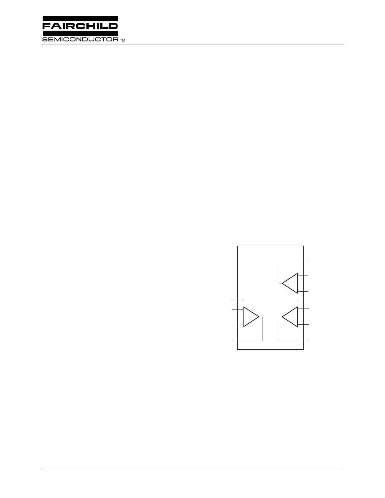
The RC6333 consists of three low power, wide band voltage
feedback operational amplifiers. Each channel is capable of
delivering a load current of at least 35mA.
The amplifiers are optimized for video applications where
low differential gain and low phase distortion are significant
requirements.
Applications
• RGB amplifiers
• Video instrumentation amplifier
• Selectable gain amplifier
• Active filters
• Set-top Buffers/Drivers
Block Diagram
RC6333
V
CC
IN1+
IN1–
+
–
OUT2
IN2-
–
+
IN2+
V
EE
IN3+
+
–
IN3–
OUT1
OUT3
65-3528-01
Rev. 1.0.1
Page 2
1
PRODUCT SPECIFICATION RC6333
Pin Assignments
RC6333
NC
NC
NC
V
CC
IN1+
IN1–
OUT1
1
2
3
4
5
6
7
65-3528-02
OUT2
14
13
IN2–
IN2+
12
V
11
10
9
8
EE
IN3+
IN3–
OUT3
Absolute Maximum Ratings
(beyond which the device may be damaged)
Pin Definitions
Pin
Name
IN1– 6 Amplifier 1 inverting input
IN1+ 5 Amplifier 1 non-inverting input
IN2– 13 Amplifier 2 inverting input
IN2+ 12 Amplifier 2 non-inverting input
IN3– 9 Amplifier 3 inverting input
IN3+ 10 Amplifier 3 non-inverting input
NC 1–3 Not Connected.
OUT1 7 Amplifier 1 output
OUT2 14 Amplifier 2 output
OUT3 8 Amplifier 3 output
V
CC
V
EE
Pin
Pin Function Description
Number
4 Analog positive supply
11 Analog negative supply
Parameter Min Typ Max Units
V
CC
V
EE
Positive power supply 7 V
Negative power supply -7 V
Differential input voltage 10 V
Operating Temperature 0 +70
Storage Temperature -40
±
125
Junction Temperature 150
Lead Soldering (10 seconds) 240
Short circuit tolerance:
No more than one output can be shorted to ground.
Notes:
1. Functional operation under any of these conditions is NOT implied.
Operating Conditions
Parameter Min Typ Max Units
V
CC
V
EE
q
JA
Power Supply Voltage 4.75 5.0 5.25 V
Negative Supply Voltage -4.75 -5.0 -5.25 V
SO14 Thermal Resistance 105
°
°
°
°
°
C/W
C
C
C
C
2
Page 3
W
RC6333 PRODUCT SPECIFICATION
DC Characteristics
W
V
CC
= 5V, V
= -5V, A
EE
= 2, R
V
LOAD
= 150
, T
Parameter Conditions Min Typ Max Units
V
OS
D
V
OS
I
B
/
D
I
B
Rin Input Resistance
Cin Input Capacitance
Input Offset Voltage No Load 3
/
D
T Offset Voltage Drift
1
Input Bias Current
D
T Input Bias Current Drift
1
1
1
CMIR Common Mode Input Range
CMRR Common Mode Rejection Ratio No Load 70 100 dB
PSRR Power Supply Rejection Ratio No Load 65 80 dB
Is Quiescent Supply Current No Load 26 40 mA
R
OUT
I
OUT
V
OUT
A
VOL
Note:
1. Guaranteed by design.
Output Impedance (Closed Loop)
Output Current Per Amplifier 35 mA
Output Voltage Swing No Load
Open-loop Gain 60 75 dB
°
A
= 0
C to 70
°
C, unless otherwise specified. Open Loop.
±
1
Enabled, At DC 0.2
±
= 150
R
L
±
±
10 mV
±
6
±
1
±
8
1M
±
30
±
5
±
40 nA/
m
V/
°
C
m
A
°
C
W
0.5 2 pF
2.5 V
W
2.5
2.5
±
3.0 V
±
3.0 V
°
AC Characteristics
C
= 10 pF, unless otherwise specified. Closed Loop. Guaranteed by Design. See Typical Test Circuit.
L
V
= 5V, V
CC
= -5V, A
EE
= 2, T
V
= 0 to 70
A
C, R
LOAD
= 150
W
, R
G
= R
F
= 250
W
Parameter Conditions Min Typ Max Units
Frequency Response
BW -3 dB Bandwidth (A
Flat
±
0.1 dB Bandwidth V
Peak Maximum Small Signal AC
= 2) V
V
= 0.4 Vpp +175 MHz
OUT
V
= 0.8 Vpp 75 90 MHz
OUT
= 0.4 Vpp 50 75 MHz
OUT
V
= 0.8 Vpp 0.01 dB
OUT
Peaking
X
TALK
Crosstalk Isolation @ 5 MHz 50 dB
Time Domain Response
t
, t
r1
Rise and Fall Time 10% to 90% 2V Output Step 10 15 ns
f1
ts Settling Time to 0.1% 2V Output Step 15 ns
OS Overshoot 2V Output Step 5 %
US Undershoot 2V Output Step 2 %
SR Slew Rate V
= ±2.0V 200 250 V/ms
OUT
Distortion
HD
HD
2
3
2nd Harmonic Dist. @ 20 MHz V
3nd Harmonic Dist. @ 20 MHz V
= 0.8 Vpp -48 dB
OUT
= 0.8 Vpp -56 dB
OUT
Video Performance
DG Diff. Gain (p-p), NTSC & PAL RL = 150W, V
DP Diff. Phase (p-p), NTSC & PAL RL = 150W, V
= ±1.5V 0.06 %
OUT
= ±1.5V 0.06 Deg.
OUT
NF Noise Floor >100kHz -130 dB rms
,
3
Page 4

PRODUCT SPECIFICATION RC6333
Test Circuit
Video
Input
R
G
250W
Applications Discussion
Capacitive Load
The RC6333 can drive a capacitive load from 10 to over 50
pF. In back terminated video applications, bandwidth will
only be limited by the RC time constants of the external output components. When driving a 75W cable, place the 75W
source termination resistor as close to the amplifier output as
possible.
DC Accuracy
Since the RC6333 is a voltage-feedback amplifier, the inverting and non-inverting inputs have similar impedances and
bias currents. To minimize offset voltage, match the source
resistances seen by inverting and non-inverting inputs.
1/3
RC6333
R
F
250W
R
S
75W
R
75W
L
R
LOAD
Video
Output
10 pF
C
L
= RL + R
65-3528-04
S
Feedback Components
Because the RC6333 is a voltage-feedback amplifier, it facilitates using reactive (capacitive and inductive) feedback
components for implementing filters, integrators, sample/
hold circuits, etc. The feedback network and the parasitic
capacitance at the inverting (summing junction) input create
a pole and affect the transfer function of the circuit. For stable operation, minimize the parasitic capacitance and equivalent resistance of the components used in the feedback
circuit.
Circuit Board
High-frequency applications require good grounding, power
supply decoupling, low parasitic capacitance and inductance,
and good isolation between the inputs to minimize their
crosstalk. Avoid coupling from output to input to prevent
positive feedback.
4
Page 5

RC6333 PRODUCT SPECIFICATION
Notes:
5
Page 6

PRODUCT SPECIFICATION RC6333
Notes:
6
Page 7

RC6333 PRODUCT SPECIFICATION
Mechanical Dimensions – 14 Pin SOIC Package
Symbol
A .053 .069 1.35 1.75
A1 .004 .010 0.10 0.25
B .013 0.33
C .008 .010 0.19 0.25
D .336 .345 8.54 8.76
E .150 .158 3.81 4.01
e
H
h
L .016 .050 0.40 1.27
N14 14
a
ccc .004 0.10——
14 8
17
Inches
Min. Max. Min. Max.
.020 0.51
.050 BSC 1.27 BSC
.228 .244 5.79 6.20
.010 .020 0.25 0.50
0¡ 8¡ 0¡ 8¡
Millimeters
EH
Notes
Notes:
1.
Dimensioning and tolerancing per ANSI Y14.5M-1982.
2.
"D" and "E" do not include mold flash. Mold flash or protrusions
shall not exceed .010 inch (0.25mm).
3.
"L" is the length of terminal for soldering to a substrate.
4.
5
2
2
3
6
Terminal numbers are shown for reference only.
5.
"C" dimension does not include solder finish thickness.
6.
Symbol "N" is the maximum number of terminals.
D
A
e
A1
SEATING
B
PLANE
– C –
LEAD COPLANARITY
ccc C
a
h x 45¡
C
L
7
Page 8

PRODUCT SPECIFICATION RC6333
Ordering Information
Product Number Temperature Range Screening Package Package Marking
RC6333M 0° to 70°C Commercial 14 Pin Narrow SOIC RC6333M
LIFE SUPPORT POLICY
FAIRCHILD’S PRODUCTS ARE NOT AUTHORIZED FOR USE AS CRITICAL COMPONENTS IN LIFE SUPPORT DEVICES
OR SYSTEMS WITHOUT THE EXPRESS WRITTEN APPROVAL OF THE PRESIDENT OF FAIRCHILD SEMICONDUCTOR
CORPORATION. As used herein:
1.Life support devices or systems are devices or systems
which, (a) are intended for surgical implant into the body,
or (b) support or sustain life, and (c) whose failure to
perform when properly used in accordance with
2.A critical component in any component of a life support
device or system whose failure to perform can be
reasonably expected to cause the failure of the life support
device or system, or to affect its safety or effectiveness.
instructions for use provided in the labeling, can be
reasonably expected to result in a significant injury of the
user.
www.fairchildsemi.com
5/20/98 0.0m 001
Ó 1998 Fairchild Semiconductor Corporation
Stock#DS30006333
 Loading...