

Page 1

DATA SH EET
Product specification
Supersedes data of 1997 Nov 26
File under Integrated Circuits, IC19
1998 Oct 14
INTEGRATED CIRCUITS
OQ2538HP; OQ2538U
SDH/SONET STM16/OC48 main
amplifiers
Page 2
1998 Oct 14 2
Philips Semiconductors Product specification
SDH/SONET STM16/OC48 main amplifiers OQ2538HP; OQ2538U
FEATURES
• Differential 100 Ω outputs for direct connection to
Current-Mode Logic (CML) inputs
• Wide bandwidth (3 GHz)
• 48.5 dB limiting gain
• Noise figure typically 11 dB
• Automatic offset compensation
• Input level-detection circuits for Automatic Gain Control
(AGC) and Loss Of Signal (LOS) detection
• Low power dissipation (typically 270 mW)
• Single −4.5 V supply voltage
• Low cost LQFP48 plastic package.
APPLICATIONS
• Main amplifier in Synchronous Digital Hierarchy (SDH)
and Synchronous Optical Network (SONET) systems for
short, medium and long haul optical transmission
• Level detector for laser diode control loops
• Wideband RF gain block with internal level detectors.
GENERAL DESCRIPTION
The OQ2538HP is a limiting amplifier IC intended for use
as the main amplifier in 2.5 Gbits/s Non-Return to Zero
(NRZ) transmission systems (SDH/SONET).
Comprised of four amplifier stages with a total gain of
48.5 dB, it provides for a wide input signal dynamic range
at a constant CML-compatible output level.
Two level-detection circuits are provided for monitoring
AGC and LOS input signal levels. An internal automatic
offset compensation circuit eliminates offset in the
amplifier chain.
ORDERING INFORMATION
TYPE
NUMBER
PACKAGE
NAME DESCRIPTION VERSION
OQ2538HP LQFP48 plastic low profile quad flat package; 48 leads; body 7 × 7 × 1.4 mm SOT313-2
OQ2538U − bare die; dimensions 2070 × 2070 × 380 µm −
Page 3

1998 Oct 14 3
Philips Semiconductors Product specification
SDH/SONET STM16/OC48 main amplifiers OQ2538HP; OQ2538U
BLOCK DIAGRAM
Fig.1 Block diagram.
handbook, full pagewidth
MGE745
AMP A AMP B AMP C AMP D
B
IN
INQ
REF
V
EE
COFF COFFQ GND
OUT
OUTQ
8
6
4521
CAPA
22 44
32
LOSDC
18
LOS
AGCDC
AGC
19
A
43
3
30
reference
voltage
for all cells
BAND GAP
OQ2538HP
Page 4
1998 Oct 14 4
Philips Semiconductors Product specification
SDH/SONET STM16/OC48 main amplifiers OQ2538HP; OQ2538U
PINNING
Notes
1. Pin type abbreviations: O = Output, I = Input, S = power Supply and A = Analog function.
2. All GND and V
EE
pads must be bonded; do not leave one single GND or VEE pad unconnected!
3. Pads denoted ‘n.c.’ should not be connected. Connections to these pads degrade device performance.
SYMBOL
PIN
(OQ2538HP)
PAD
(OQ2538U)
TYPE
(1)
DESCRIPTION
V
EE
1, 12, 13, 24, 25,
36, 37, 48
2, 3, 11, 12, 28,
29
(2)
S negative power supply
n.c. 2, 11, 14, 15, 23,
26, 27, 35, 38,
40, 46, 47
20, 22
(3)
− not connected
AGC 3 30 O rectifier A output
GND 4, 5, 7, 9, 10, 16,
17, 20, 28, 29,
31, 33, 34, 39,
41, 42
1, 4, 5, 8, 13, 14,
16, 18, 19, 21,
23, 24, 31, 32,
34, 36
(2)
S ground
INQ 6 33 I main amplifier inverting input
IN 8 35 I main amplifier input
LOSDC 18 6 O rectifier B reference output
LOS 19 7 O rectifier B output
REF 21 9 O band gap reference
CAPA 22 10 A pin for connecting band gap reference decoupling
capacitor
OUTQ 30 15 O main amplifier inverted output
OUT 32 17 O main amplifier output
AGCDC 43 25 O rectifier A reference output
COFFQ 44 26 A pin for connecting automatic offset control capacitor
(return)
COFF 45 27 A pin for connecting automatic offset control capacitor
Page 5

1998 Oct 14 5
Philips Semiconductors Product specification
SDH/SONET STM16/OC48 main amplifiers OQ2538HP; OQ2538U
Fig.2 Pin configuration.
handbook, full pagewidth
1
2
3
4
5
6
7
8
9
10
11
36
35
34
33
32
31
30
29
28
27
26
13
14
15
16
17
18
19
20
21
22
23
48
47
46
45
44
43
42
41
40
39
38
12
24 37
25
OQ2538HP
MGE744
V
EE
n.c.
GND
GND
GND
OUTQ
GND
GND
n.c.
n.c.
V
EE
V
EE
n.c.
AGC
GND
GND
INQ
IN
GND
n.c.
V
EE
OUT
n.c.
n.c.
COFF
COFFQ
AGCDC
GND
n.c.
GND
n.c.
V
EE
V
EE
GND
GND
GND
n.c.
n.c.
GND
GND
LOSDC
LOS
GND
CAPA
n.c.
V
EE
V
EE
REF
Page 6
1998 Oct 14 6
Philips Semiconductors Product specification
SDH/SONET STM16/OC48 main amplifiers OQ2538HP; OQ2538U
FUNCTIONAL DESCRIPTION
The OQ2538HP is comprised of four DC-coupled amplifier
stages along with additional circuitry for offset
compensation and level detection.
The first amplifier stage contains a modified
Cherry/Hooper amplifying cell with high gain
(approximately 20 dB) and a wide bandwidth. Special
attention is paid to minimizing the equivalent input noise at
this stage, thus reducing the overall noise level. Additional
feedback is applied at the second and third stages,
improving isolation and reducing the gain to 14 dB per
stage. The last stage is an output buffer, a unity gain
amplifier, with an output impedance of 100 Ω.
The total gain of the OQ2538HP amounts to 48.5 dB, thus
providing a constant CML-compatible output signal over a
wide input signal range.
Two rectifier circuits are used to measure the input signal
level. Two separate RF preamplifiers are used to generate
the voltage gain needed to obtain a suitable rectifier output
voltage. For rectifier A the gain is approximately 18 dB, for
rectifier B it is about 14 dB. The output of rectifier A can be
used for AGC at the preamplifier stage in front of the
OQ2538HP. The output of rectifier B can be used for LOS
detection. There is a linear relationship between the
rectifier output voltage and the input signal level provided
the amplifiers are not saturated.
Because the four gain stages are DC-coupled and provide
a high overall gain, the effect of the input offset can be
considerable. The OQ2538HP features an internal offset
compensation circuit for eliminating the input offset.
The bandwidth of the offset control loop is determined by
an external capacitor.
COFF and COFFQ offset compensation
Automatic offset compensation eliminates the input offset
of the OQ2538HP. This offset cancellation influences the
low frequency gain of the amplifier stages. With a
capacitance of 100 nF between COFF and COFFQ the
loop bandwidth will be less than 1.5 kHz, small enough to
have no influence on amplifier gain over the frequencies of
interest. If the capacitor was omitted, the loop bandwidth
would be greater than 30 MHz, which would influence the
input signal gain. The loop bandwidth can be calculated
from the following formula:
(1)
where C
ext
is the capacitance connected between COFF
and COFFQ.
f
loop
1
2π 1250Ω× C
ext
×
------------------------------------------------
=
REF and CAPA band gap output and decoupling
capacitance
To reduce band gap noise levels, a 1 nF decoupling
capacitor on CAPA is recommended. Since the band gap
is referenced to the negative power supply, the decoupling
capacitor should be connected between CAPA and V
EE
.
The band gap voltage is present on pin REF for test
purposes only. It is not intended to serve as an external
reference.
RF input and output connections
Striplines, or microstrips, with an odd mode characteristic
impedance of Z
o(odd)
=50Ω must be used for the
differential RF connections on the PCB. This applies to
both the input signal pair IN and INQ and to the output
signal pair OUT and OUTQ. The two lines in each pair
should have the same length.
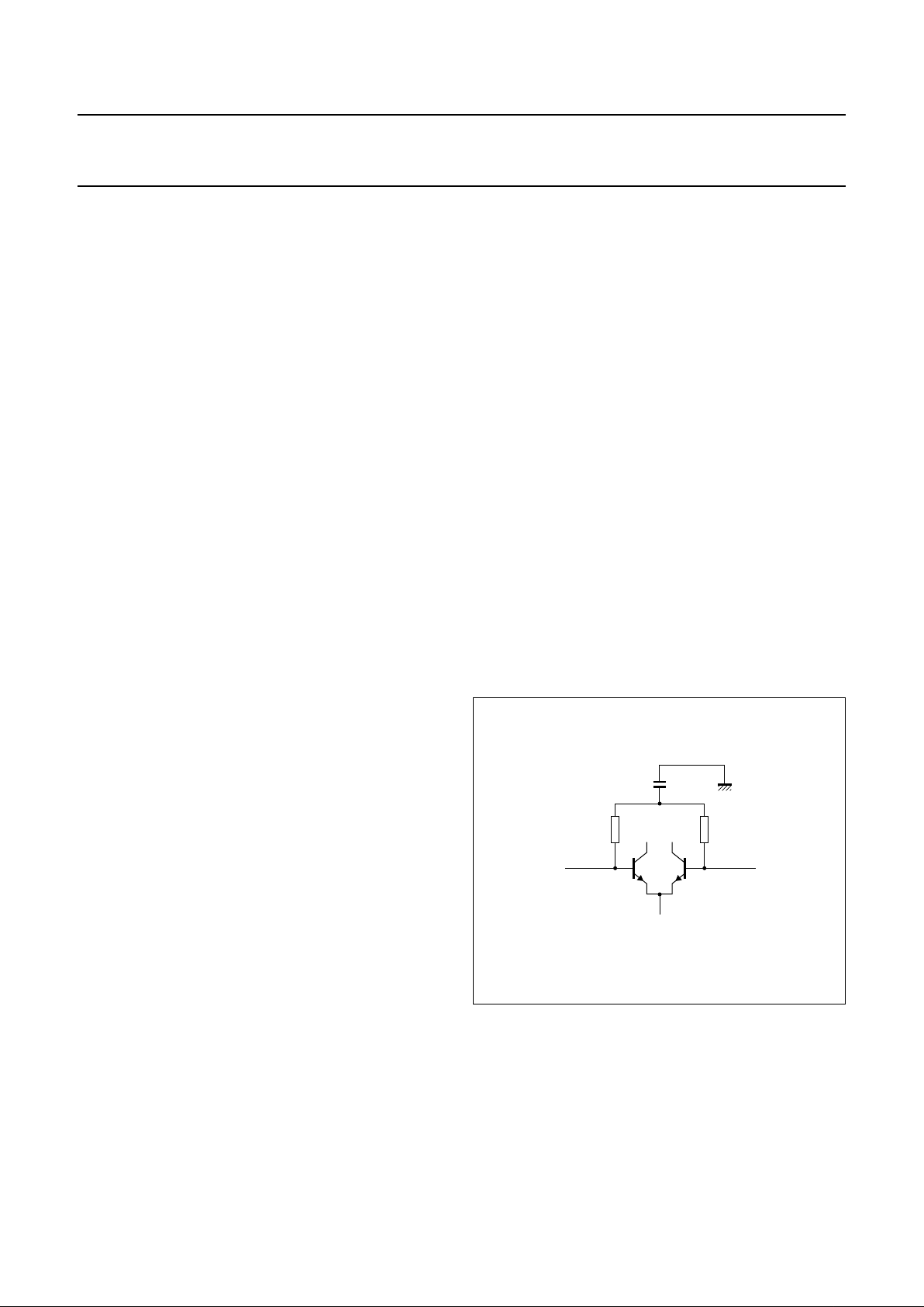
RF input matching circuit
The input circuit for pins IN and INQ contains internal
100 Ω resistors decoupled to ground via an internal
common mode 6 pF capacitor. The topology is depicted in
Fig.3.
Fig.3 RF input topology.
handbook, halfpage
MGM114
IN INQ
GND
100 Ω
6 pF
100 Ω
Page 7
1998 Oct 14 7
Philips Semiconductors Product specification
SDH/SONET STM16/OC48 main amplifiers OQ2538HP; OQ2538U
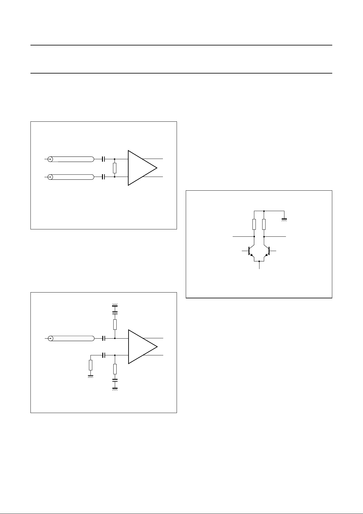
An external 200 Ω resistor between IN and INQ is
recommended in order to match the inputs to a differential
transmission line, coupled microstrip or stripline with an
odd mode impedance Z
o(odd)
=50Ω, as shown in Fig.4.
For single-ended excitation, separate matching networks
on IN and INQ, as depicted in Fig.5, achieve optimum
matching. Care should be taken to avoid DC loading, since
the OQ2538HP controls its own DC input voltage.
The resistors on the unused input INQ may be combined
for convenience.
In both cases, the essence of good matching is the equity
of the circuitry on both input pins. The impedance seen on
pins IN and INQ should be as equal as possible. For more
information see
“Application Note AN96051
” describing
the OM5801 STM16 demo board.
Fig.4 Differential input matching.
handbook, halfpage
differential line
Z
o(odd)
= 50 Ω
MGM115
200 Ω
IN
INQ
22 nF
22 nF
Fig.5 Single-ended input matching.
handbook, halfpage
MGM116
100 Ω
100 Ω
50 Ω
IN
INQ
22 nF
22 nF
22 nF
22 nF
Zo = 50 Ω
transmission line
RF output matching circuit
Matching of the main amplifier outputs, OUT and OUTQ, is
not mandatory. In most applications, the receiving end of
the transmission line will be properly matched, so very little
reflection will occur. Matching the transmitting end to
absorb these reflections is only recommended for very
sensitive applications. In such cases, 100 Ω pull-up
resistors should be connected from OUT and OUTQ to
ground, as close as possible to the IC pins. These
matching resistors will not be needed in most applications,
however. The output circuit of the OQ2538HP is depicted
in Fig.6. For more information see
“Application Note
AN96051”
describing the OM5801 STM16 demo board.
Fig.6 RF output topology.
handbook, halfpage
MGM117
OUT
OUTQ
GND
100 Ω 100 Ω
Page 8
1998 Oct 14 8
Philips Semiconductors Product specification
SDH/SONET STM16/OC48 main amplifiers OQ2538HP; OQ2538U
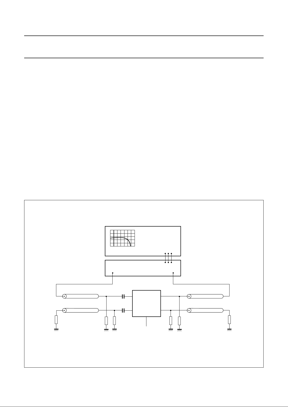
RF gain and group delay measurements
The measurement set-up shown in Fig.7 was used to
measure the single-ended small signal gain as specified in
Chapter “Characteristics”. Since the network analyzer can
only perform single-ended measurements, the
single-ended matching scheme described above is used
to match the inputs of the OQ2538HP to 50 Ω. For greater
accuracy, the outputs are also matched. The gain
measured with this set-up is denoted by S21. Graphs of
typical S21 and group delay characteristics are shown in
Figs 8 and 9. The OQ2538HP test PCB used for these
measurements can be supplied on request.
Although the differential voltage gain of the OQ2538HP
cannot be measured directly, it can be calculated from S
21
.
The differential voltage gain is 6 dB greater than the
measured S21 value, typically 46 dB (40 + 6 dB). If the
100 Ω matching resistors on the output are omitted, the
differential voltage gain is increased by a further 2.4 dB,
typically to 48.4 dB. This is due to the fact that the output
load is increased from 25 to 33 Ω, so the output voltage is
increased by a factor of 1.32 (2.4 dB).
When performing S
21
measurements make sure the input
power level is around −50 dBm, as indicated in Fig.7
(port 1 of the network analyzer). For correct measurement
results the OQ2538 should not be limiting the input signal,
but operate in its linear region. This can be achieved by
using a very small input signal level of −50 dBm.
Fig.7 S21 and group delay measurement set-up.
handbook, full pagewidth
MGM111
100 Ω
50 Ω SMA
termination
IN
INQ
OUT
OUTQ
100 pF
100 pF
50 Ω semi rigid
100 Ω
100 Ω 100 Ω
50 Ω SMA
termination
50 Ω semi rigid
50 Ω semi rigid
50 Ω semi rigid
OQ2538HP
test PCB
P = 50 dBm
S-PARAMETER TEST SET
6 GHz NETWORK ANALYZER
PORT 1 PORT 2
V
EE
= −4.5 V
Zo = 50 Ω
Zo = 50 Ω
Page 9
1998 Oct 14 9
Philips Semiconductors Product specification
SDH/SONET STM16/OC48 main amplifiers OQ2538HP; OQ2538U
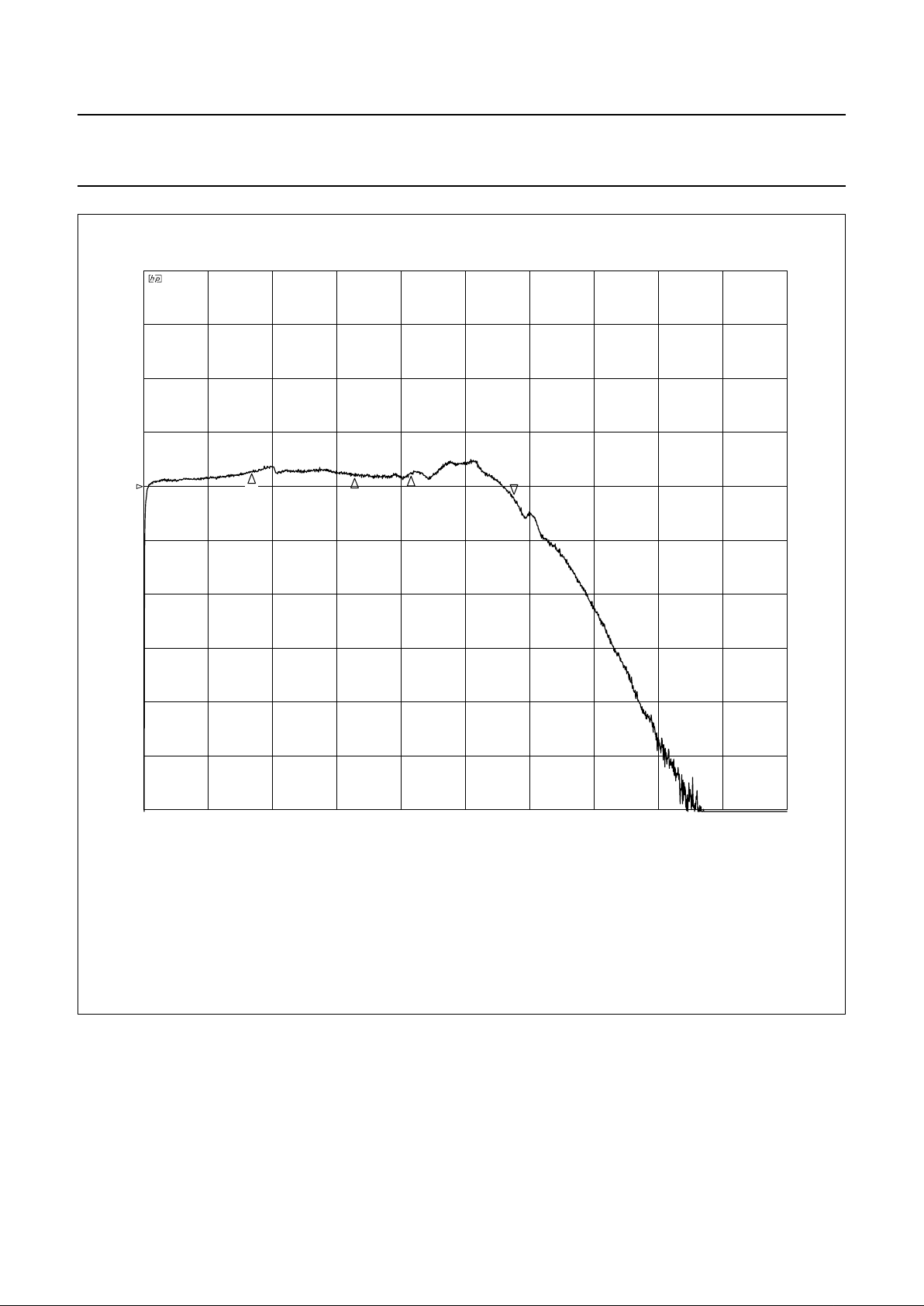
Fig.8 S21 characteristic, measured on the OQ2538HP test PCB.
handbook, full pagewidth
MGM160
start: 30 kHz
S21 log MAG
40 dB
stop: 6 GHz
(2)
(4)
(3)
(1)
Vertical scale 6 dB/division.
Linear frequency sweep; start: 30 kHz; stop: 6 GHz.
(1) 41.603 dB; 1 GHz.
(2) 38.633 dB; 3.45 GHz.
(3) 41.291 dB; 2 GHz.
(4) 41.386 dB; 2.5 GHz.
Page 10

1998 Oct 14 10
Philips Semiconductors Product specification
SDH/SONET STM16/OC48 main amplifiers OQ2538HP; OQ2538U
Fig.9 Group delay characteristic, measured on the OQ2538HP test PCB.
handbook, full pagewidth
MGM161
start: 30 kHz
S21 delay
0 ps
stop: 6 GHz
(2)
(4)
(3)
(1)
Vertical scale 200 ps/division.
Linear frequency sweep; start: 30 kHz; stop: 6 GHz.
(1) 832.91 ps; 1 GHz.
(2) 1007.4 ps; 3.45 GHz.
(3) 834 ps; 2 GHz.
(4) 860.93 ps; 2.5 GHz.
Page 11
1998 Oct 14 11
Philips Semiconductors Product specification
SDH/SONET STM16/OC48 main amplifiers OQ2538HP; OQ2538U
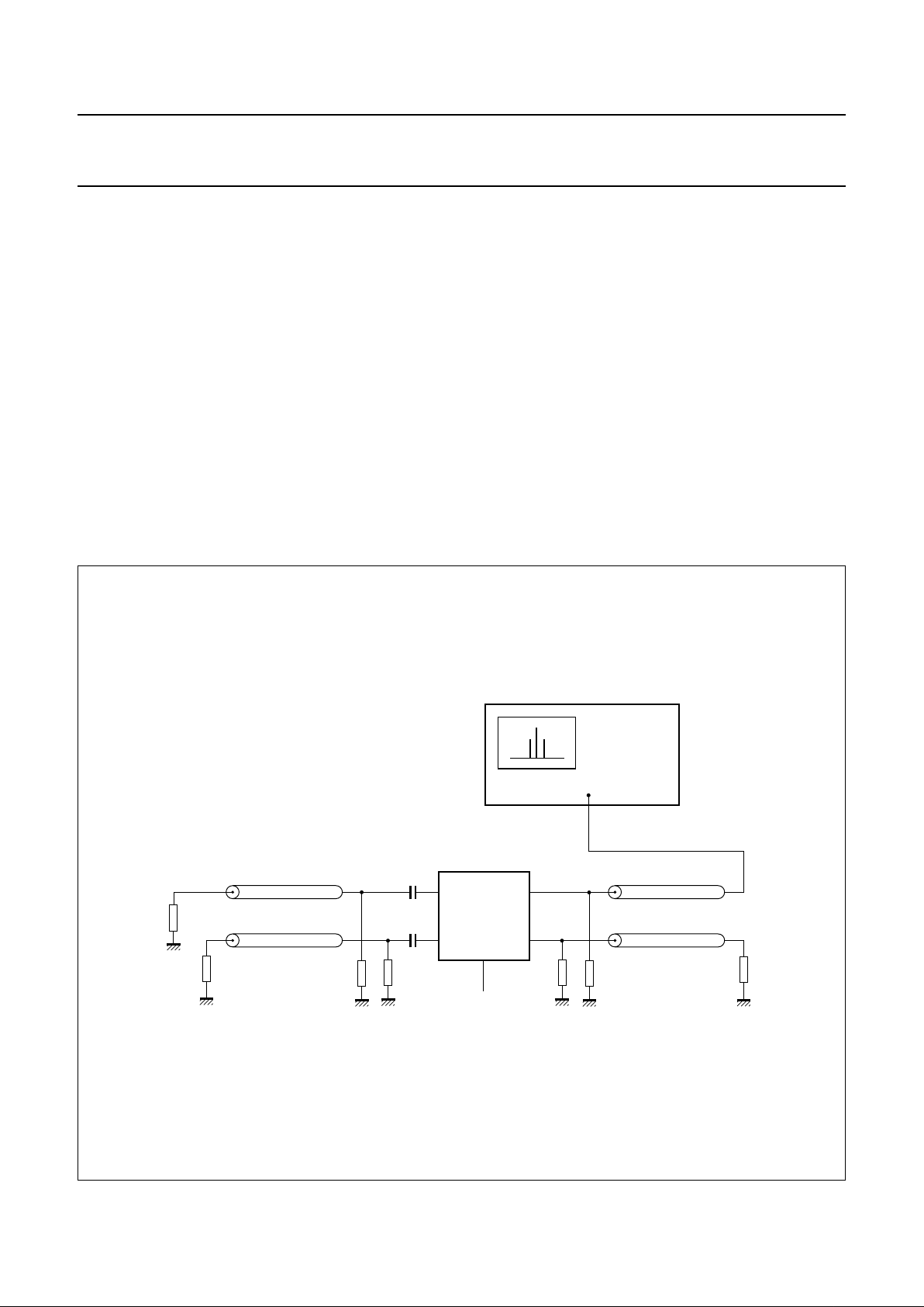
Noise figure measurements
The noise figure is the ratio of signal-to-noise ratio at the
input (S
i/Ni
) to signal-to-noise ratio at the output (So/No) of
the amplifier. This definition is true for both single-ended
and differential amplifiers, provided the correct values for
S
i/Ni
and So/No are substituted in the formula. The noise
figure is measured using the differential set-up shown in
Fig.10. The total noise on the output (N
o
in dBm) is
measured using the spectrum analyzer at the frequency of
interest. From this value, the actual (differential) noise
figure for that frequency (spot noise figure) can be
calculated using the following formula:
The factor 2 in the denominator is present to compensate
for the fact that S
21
is the single-ended power gain,
F
S
iNi
⁄
S
oNo
⁄
-----------------
N
o
2S⋅21Ni⋅
-------------------------- -
N
o
2S⋅21kT⋅
----------------------------
== =
whereas the differential power gain is applicable in this
situation. N
i
can be replaced with the available noise
power at the input, which is kT under matched conditions
(k is Boltzmann’s constant). The formula expressed in
dBm makes calculation easier:
,
assuming log(kT) is −173.8 dBm (T = 298 K) and
N
o
measured in 1 Hz bandwidth and expressed in dBm.
For the OQ2538HP, in the differential configuration
(including the 100 Ω matching resistors), this yields a
typical noise figure of 11 dB.
While the performance of this measurement set-up cannot
match that of a dedicated noise analysis system, the
results are comparable for an amplifier with a noise figure
of 11 dB.
FN
o
= S213+()173.8+– dB[]
Fig.10 Noise figure measurement set-up.
handbook, full pagewidth
MGM112
100 Ω
50 Ω SMA
termination
IN
INQ
OUT
OUTQ
100 pF
100 pF
50 Ω semi rigid
100 Ω
100 Ω
100 Ω
50 Ω SMA
termination
50 Ω SMA
termination
50 Ω semi rigid
50 Ω semi rigid
50 Ω semi rigid
OQ2538HP
test PCB
IN
SPECTRUM
ANALYZER
Zo = 50 Ω
V
EE
= −4.5 V
Page 12

1998 Oct 14 12
Philips Semiconductors Product specification
SDH/SONET STM16/OC48 main amplifiers OQ2538HP; OQ2538U
Fig.11 AGC transfer characteristics.
(1) T
amb
= −20 °C.
(2) T
amb
= +25 °C.
(3) T
amb
= +85 °C.
MGE746
0
100 203040
100
200
60 80
V
AGC
− V
AGCDC
(mV)
50
V
IN
(mV p-p)
(1)
(2)
(3)
Fig.12 LOS detection characteristics.
(1) T
amb
= −20 °C.
(2) T
amb
= +25 °C.
(3) T
amb
= +85 °C.
0
100
200
V
IN
(mV p-p)
10 357246810119
V
LOS
− V
LOSDC
(mV)
MGE747
(1)
(2)
(3)
AGC and AGCDC level detection
When using rectifier A as an input signal level detector, the
AGC and AGCDC pins must be decoupled to ground with
100 nF capacitors. The AGCDC output is intended as a
reference voltage against which the actual AGC output
voltage can be compared. This voltage difference,
V
AGC
− V
AGCDC
, can be used as a control input in an AGC
loop. A graph depicting output voltage difference as a
function of the input signal level (typical) is shown in
Fig.11. Note that an input signal with the specified
peak-to-peak value is applied to both IN and INQ inputs,
but with complementary phase.
LOS and LOSDC level detection
The output of rectifier B can be used for LOS detection.
The LOSDC output provides a reference voltage against
which the voltage at the LOS output can be compared.
The voltage difference V
LOS
− V
LOSDC
can be used as
input to a LOS detection circuit. Both outputs need to be
decoupled using 100 nF capacitors. A graph depicting
V
LOS
− V
LOSDC
as a function of the input signal level
(typical) is shown in Fig.12. Note that an input signal with
the specified peak-to-peak value is applied to both IN and
INQ inputs, but with complementary phase.
Grounding and power supply decoupling
The ground connection on the PCB needs to be a large
copper area fill connected to a common ground plane with
as low inductance as possible, preferably positioned
directly underneath the LQFP48 package. The large area
fill will improve heat transfer to the PCB and thus aid IC
cooling.
All V
EE
pins (two at each corner) need to be connected to
a common supply plane with as low inductance as
possible. This plane should be decoupled to ground.
To avoid high frequency resonance, multiple bypass
capacitors should not be mounted at the same location.
To minimize low frequency switching noise in the vicinity of
the OQ2538HP, the power supply line should be filtered
once using an LC-circuit with a low cut-off frequency
(see Fig.14).
Page 13

1998 Oct 14 13
Philips Semiconductors Product specification
SDH/SONET STM16/OC48 main amplifiers OQ2538HP; OQ2538U
Using alternative supply voltages
Although the OQ2538HP is intended to be used with a
single −4.5 V supply voltage, a slightly modified −5V
supply can also be used. By connecting a Schottky diode
between the VEE power supply line and the IC, an
additional 0.5 V voltage drop is obtained, bringing the
supply voltage on the pins of the OQ2538HP within the
specified range. A BAS85 Schottky diode is
recommended. A −5 V application schematic is shown in
Fig.15.
Extrapolating from this case, a +5 V application is also
possible. However, care should be taken with the RF
transmission lines. The on-chip signals refer to the GND
pins, which become the positive supply pins in a +5 V
application. The external transmission lines will most likely
be referenced to system ground (V
EE
pins). The RF signals
will change from one reference plane to another at the
interface to the RF input and output pins. The positive
supply application is very vulnerable to interference at this
point. For a successful +5 V application, special care
should be taken when designing board layout to reduce
the influence of interference and keep the positive supply
as clean as possible.
ESD protection
Exceptions have been made to the standard ESD
protection scheme in order to achieve high frequency
performance. The inputs IN and INQ and the outputs OUT
and OUTQ haveno protection against ESD. All other pins
have a standard ESD protection structure, capable of
withstanding 2 kV Human Body Model (HBM) zappings.
Page 14

1998 Oct 14 14
Philips Semiconductors Product specification
SDH/SONET STM16/OC48 main amplifiers OQ2538HP; OQ2538U
LIMITING VALUES
In accordance with the Absolute Maximum Rating System (IEC 134).
Note
1. ∆V
I=VIN
− V
INQ
(AC only). The DC level is internally controlled.
HANDLING
Precautions should be taken to avoid damage through electrostatic discharge. This is particularly important during
assembly and handling of the bare die. Additional safety can be obtained by bonding the V
EE
and GND pads first, the
remaining pads may then be bonded to their external connections in any order (see also Section “ESD protection”).
THERMAL CHARACTERISTICS
Note
1. R
th(j-a)
will be in the application from 15 to 65 K/W, dependent on the PCB layout.
SYMBOL PARAMETER CONDITIONS MIN. MAX. UNIT
V
EE
negative supply voltage −6.0 +0.5 V
∆V
I
input voltage difference note 1 −600 +600 mV
I
IN
, I
INQ
input current −2.0 +2.0 mA
I
n
DC current
pins 30 and 32 −6 +10 mA
pins 3, 18, 19 and 43 −3+3mA
pin 21 −2+2mA
pins 44 and 45 −1+1mA
pin 22 −0.1 +0.1 mA
P
tot
total power dissipation − 380 mW
T
j
junction temperature − 150 °C
T
stg
storage temperature −65 +150 °C
SYMBOL DESCRIPTION CONDITIONS VALUE UNIT
R
th(j-s)
thermal resistance from junction to solder point 15 K/W
R
th(j-a)
thermal resistance from junction to ambient note 1 65 K/W
Page 15

1998 Oct 14 15
Philips Semiconductors Product specification
SDH/SONET STM16/OC48 main amplifiers OQ2538HP; OQ2538U
CHARACTERISTICS
At nominal supply voltages; T
amb
= −40 to +85 °C; 50 Ω measuring environment.
SYMBOL PARAMETER CONDITIONS MIN. TYP. MAX. UNIT
V
EE
negative supply voltage −4.725 −4.5 −4.275 V
I
EE
negative supply current − 60 80 mA
P
tot
total power dissipation note 1 − 270 380 mW
T
amb
operating ambient temperature note 2 −40 − +85 °C
T
j
operating junction temperature −40 − +120 °C
Main amplifier inputs: IN and INQ; note 3
V
i(sens)
input sensitivity note 4 − 0.5 2.5 mV
V
i(p-p)
signal voltage swing (peak-to-peak
value)
note 4 2.5 − 600 mV
V
I
DC input voltage note 5 −2.4 −2.1 −1.7 V
V
IO
input offset voltage note 6 − 0.2 − mV
Z
i
single-ended input impedance note 7 − 100 −Ω
S
21
single-ended small signal gain note 8 34 40 − dB
G
v(dif)
differential voltage gain note 9 − 48.5 − dB
N
o
output noise power note 10 −−120 − dBm
F noise figure note 10 − 11 − dB
B
−3dB
3 dB bandwidth 2.4 3.0 − GHz
Rectifier outputs: AGC and AGCDC; note 11
V
O(ref)
DC reference voltage open output −3.3 −3.0 −2.5 V
V
i(p-p)
input voltages on pins IN and INQ for
linear rectifier output (peak-to-peak
value)
12.5 − 60 mV
∆V maximum input signal level related
voltage difference
note 12 − 400 − mV
V
OO
output offset voltage note 13 −5 − +5 mV
Rectifier outputs: LOS and LOSDC; note 11
V
O(ref)
DC reference voltage open output −3.4 −3.1 −2.6 V
V
i(p-p)
input voltages on pins IN and INQ for
linear recitifier output (peak-to-peak
value)
2.5 − 9mV
∆V maximum input signal level related
voltage difference
note 12 − 450 − mV
V
OO
output offset voltage note 13 −15 − +15 mV
Automatic offset compensation lowpass filter: COFF and COFFQ
V
O
DC output voltage open output −2.4 −2.1 −1.7 V
R offset compensation filter resistance − 1250 −Ω
Band gap reference: REF
V
O
band gap voltage referenced to VEE;
open output; note 14
1.1 1.3 1.5 V
Page 16
1998 Oct 14 16
Philips Semiconductors Product specification
SDH/SONET STM16/OC48 main amplifiers OQ2538HP; OQ2538U
Notes
1. No special cooling is required in the application if the total thermal resistance R
th(j-a)
is less than 90 K/W.
2. The temperature of the PCB in the vicinity of the IC is taken to be the ambient temperature.
3. The input signal must be AC-coupled to the inputs through a coupling capacitance >22 nF.
4. V
i(p-p)
is the input signal on IN and INQ for full output clipping. It is assumed that both inputs carry a complementary
signal of the specified peak-to-peak value. The lower specified limit is usually called the input sensitivity. This value
is defined as a 20% increase in rise and fall times when compared to rise and fall times with a complementary input
signal of 10 mV (p-p) applied to IN and INQ.
5. The DC voltage is fixed internally; only AC-coupling of the input signal is allowed.
6. VIO= V
IN
− V
INQ
7. See Section “RF input matching circuit” for detailed information.
8. All signal ports are AC-matched to 50 Ω and are measured at 1 GHz (see Fig.7). Flatness deviations are within ±3dB
over the entire bandwidth.
9. See Section “RF gain and group delay measurements”.
10. F is the noise figure for a differential application and is measured at 1 GHz. See Section “Noise figure
measurements”.
11. An external 100 nF capacitor is connected at each output to remove any spurious high frequency signals.
Any circuitry driven from these pins must have an input impedance >50 kΩ.
12. Voltage difference between AGC (LOS) and AGCDC (LOSDC), measured with a differential square wave input
signal of 600 mV (p-p) on IN and INQ.
13. The offset is measured with inputs IN and INQ shorted together.
14. The band gap voltage may not be used as an external reference.
15. Both outputs are connected to ground through a 50 Ω load resistance and carry complementary signals.
16. The output levels are dependent on load impedance. The specified values assume an external load impedance of
50 Ω. If the external 100 Ω matching resistors are connected at pins OUT and OUTQ, the output levels will fall to
75% of the specified values (see also Section “RF gain and group delay measurements”).
Band gap reference decoupling: CAPA
V
O
decoupling voltage referenced to VEE;
open output
− 2.9 − V
Main amplifier outputs: OUT and OUTQ; note 15
V
OH
HIGH-level output voltage −20 −50 mV
V
OL
LOW-level output voltage note 16 −280 −200 −140 mV
t
r
differential output rise time input signal >2.5 mV (p-p) − 100 150 ps
t
f
differential output fall time input signal >2.5 mV (p-p) − 100 150 ps
Z
o
single-ended output impedance see Fig.6 83 100 117 Ω
SYMBOL PARAMETER CONDITIONS MIN. TYP. MAX. UNIT
Page 17

1998 Oct 14 17
Philips Semiconductors Product specification
SDH/SONET STM16/OC48 main amplifiers OQ2538HP; OQ2538U
APPLICATION INFORMATION
Fig.13 System application diagram.
handbook, full pagewidth
MGE748
I
PHOTO
V
bias
PHOTODIODE
R
FB
TRANS-
IMPEDANCE
AMPLIFIER
LIMITING
AMPLIFIER
DATA AND
CLOCK
RECOVERY
FILTER
CGY2100
OQ2538HP
OQ2541HP
to data and
clock recovery unit
data
recovered
clock
Fig.14 Typical application schematic.
handbook, full pagewidth
MGE749
10 µH
1 nF
100
nF
4.7
µF
100nF100
nF
33
nF
100
nF
100
nF
OQ2538HP
IN
INQ
IN
8
16
3
43
19 18
22
21
44
45
30
32
C
IN
C
INQ
INQ
AGC
LOS LOSDC
V
EE
GND
AGCDC
OUT
OUTQ
COFFQ
COFF
REF
CAPA
GAIN
REGULATION
LOSS OF SIGNAL
DETECTION
−4.5 V
200 Ω
>22 nF
>22 nF
V
EE
Page 18

1998 Oct 14 18
Philips Semiconductors Product specification
SDH/SONET STM16/OC48 main amplifiers OQ2538HP; OQ2538U
Fig.15 −5 V application schematic.
handbook, full pagewidth
MGM113
10 µH
1 nF
100
nF
4.7
µF
100nF100
nF
33
nF
100
nF
100
nF
OQ2538HP
IN
INQ
IN
8
16
3
43
19 18
22
21
44
45
30
32
C
IN
C
INQ
INQ
AGC
LOS LOSDC
V
EE
GND
AGCDC
OUT
OUTQ
COFFQ
COFF
REF
CAPA
GAIN
REGULATION
LOSS OF SIGNAL
DETECTION
−5.0 V
200 Ω
>22 nF
>22 nF
V
EE
BAS85
Page 19

1998 Oct 14 19
Philips Semiconductors Product specification
SDH/SONET STM16/OC48 main amplifiers OQ2538HP; OQ2538U
BONDING PAD LOCATIONS
Fig.16 Bonding pad locations of OQ2538U.
(1) Typical value.
handbook, full pagewidth
1
2 3 4 5 6 7 8 9 10 11
12
13
14
15
16
17
18
19
20212223242526272829
30
31
32
33
34
35
36
GND
GND
GND
GND
GND
INQ
IN
V
EE
V
EE
GND
GND
OUTQ
GND
OUT
GND
GND
n.c.
n.c.
GND
GND
GND
AGCDC
COFFQ
COFF
V
EE
V
EE
GND
GND
GND
REF
CAPA
LOSDC
LOS
MGR525
2.07 mm
(1)
2.07
(1)
mm
OQ2538U
x
y
0
0
AGC
V
EE
V
EE
Page 20

1998 Oct 14 20
Philips Semiconductors Product specification
SDH/SONET STM16/OC48 main amplifiers OQ2538HP; OQ2538U
Table 1 Bonding pad locations. All x/y coordinates
represent the position of the centre of the pad
with respect to the centre of the die (see
Fig.16).
SYMBOL PAD
COORDINATES
xy
GND 1 −900 −700
V
EE
2 −900 −900
V
EE
3 −700 −900
GND 4 −500 −900
GND 5 −300 −900
LOSDC 6 −100 −900
LOS 7 +100 −900
GND 8 +300 −900
REF 9 +500 −900
CAPA 10 +700 −900
V
EE
11 +900 −900
V
EE
12 +900 −700
GND 13 +900 −500
GND 14 +900 −300
OUTQ 15 +900 −100
GND 16 +900 +100
OUT 17 +900 +300
GND 18 +900 +500
GND 19 +900 +700
n.c. 20 +900 +900
GND 21 +700 +900
n.c. 22 +500 +900
GND 23 +300 +900
GND 24 +100 +900
AGCDC 25 −100 +900
COFFQ 26 −300 +900
COFF 27 −500 +900
V
EE
28 −700 +900
V
EE
29 −900 +900
AGC 30 −900 +700
GND 31 −900 +500
GND 32 −900 +300
INQ 33 −900 +100
GND 34 −900 −100
IN 35 −900 −300
GND 36 −900 −500
SYMBOL PAD
COORDINATES
xy
Table 2 Physical characteristics of bare die
PARAMETER VALUE
Glass passivation 0.8 µm silicon nitride on top of 0.9 µm PSG (PhosphoSilicate Glass)
Bonding pad dimension minimum dimension of exposed metallization is 90 × 90 µm (pad size = 100 × 100 µm)
Metallization 1.8 µm AlCu (1% Cu)
Thickness 380 µm nominal
Size 2.070 × 2.070 mm (4.285 mm
2
)
Backing silicon; electrically connected to V
EE
potential through substrate contacts
Attache temperature <440 °C; recommended die attache is glue
Attache time <15 s
Page 21

1998 Oct 14 21
Philips Semiconductors Product specification
SDH/SONET STM16/OC48 main amplifiers OQ2538HP; OQ2538U
PACKAGE OUTLINE
UNIT
A
max.
A1A2A3b
p
cE
(1)
eH
E
LL
p
Zywv θ
REFERENCES
OUTLINE
VERSION
EUROPEAN
PROJECTION
ISSUE DATE
IEC JEDEC EIAJ
mm
1.60
0.20
0.05
1.45
1.35
0.25
0.27
0.17
0.18
0.12
7.1
6.9
0.5
9.15
8.85
0.95
0.55
7
0
o
o
0.12 0.10.21.0
DIMENSIONS (mm are the original dimensions)
Note
1. Plastic or metal protrusions of 0.25 mm maximum per side are not included.
0.75
0.45
SOT313-2
94-12-19
97-08-01
D
(1) (1)(1)
7.1
6.9
H
D
9.15
8.85
E
Z
0.95
0.55
D
b
p
e
E
B
12
D
H
b
p
E
H
v M
B
D
Z
D
A
Z
E
e
v M
A
1
48
37
36
25
24
13
θ
A
1
A
L
p
detail X
L
(A )
3
A
2
X
y
c
w M
w M
0 2.5 5 mm
scale
pin 1 index
LQFP48: plastic low profile quad flat package; 48 leads; body 7 x 7 x 1.4 mm
SOT313-2
Page 22

1998 Oct 14 22
Philips Semiconductors Product specification
SDH/SONET STM16/OC48 main amplifiers OQ2538HP; OQ2538U
SOLDERING
Introduction
There is no soldering method that is ideal for all IC
packages. Wave soldering is often preferred when
through-hole and surface mounted components are mixed
on one printed-circuit board. However, wave soldering is
not always suitable for surface mounted ICs, or for
printed-circuits with high population densities. In these
situations reflow soldering is often used.
This text gives a very brief insight to a complex technology.
A more in-depth account of soldering ICs can be found in
our
“Data Handbook IC26; Integrated Circuit Packages”
(order code 9398 652 90011).
Reflow soldering
Reflow soldering techniques are suitable for all LQFP
packages.
Reflow soldering requires solder paste (a suspension of
fine solder particles, flux and binding agent) to be applied
to the printed-circuit board by screen printing, stencilling or
pressure-syringe dispensing before package placement.
Several methods exist for reflowing; for example,
infrared/convection heating in a conveyor type oven.
Throughput times (preheating, soldering and cooling) vary
between 50 and 300 seconds depending on heating
method. Typical reflow peak temperatures range from
215 to 250 °C.
Wave soldering
Wave soldering is not recommended for LQFP packages.
This is because of the likelihood of solder bridging due to
closely-spaced leads and the possibility of incomplete
solder penetration in multi-lead devices.
CAUTION
Wave soldering is NOT applicable for all LQFP
packages with a pitch (e) equal or less than 0.5 mm.
If wave soldering cannot be avoided, for LQFP
packages with a pitch (e) larger than 0.5 mm, the
following conditions must be observed:
• A double-wave (a turbulent wave with high upward
pressure followed by a smooth laminar wave)
soldering technique should be used.
• The footprint must be at an angle of 45° to the board
direction and must incorporate solder thieves
downstream and at the side corners.
During placement and before soldering, the package must
be fixed with a droplet of adhesive. The adhesive can be
applied by screen printing, pin transfer or syringe
dispensing. The package can be soldered after the
adhesive is cured.
Maximum permissible solder temperature is 260 °C, and
maximum duration of package immersion in solder is
10 seconds, if cooled to less than 150 °C within
6 seconds. Typical dwell time is 4 seconds at 250 °C.
A mildly-activated flux will eliminate the need for removal
of corrosive residues in most applications.
Repairing soldered joints
Fix the component by first soldering two diagonallyopposite end leads. Use only a low voltage soldering iron
(less than 24 V) applied to the flat part of the lead. Contact
time must be limited to 10 seconds at up to 300 °C. When
using a dedicated tool, all other leads can be soldered in
one operation within 2 to 5 seconds between
270 and 320 °C.
Page 23

1998 Oct 14 23
Philips Semiconductors Product specification
SDH/SONET STM16/OC48 main amplifiers OQ2538HP; OQ2538U
DEFINITIONS
LIFE SUPPORT APPLICATIONS
These products are not designed for use in life support appliances, devices, or systems where malfunction of these
products can reasonably be expected to result in personal injury. Philips customers using or selling these products for
use in such applications do so at their own risk and agree to fully indemnify Philips for any damages resulting from such
improper use or sale.
BARE DIE DISCLAIMER
All die are tested and are guaranteed to comply with all data sheet limits up to the point of wafer sawing for a period of
ninety (90) days from the date of Philips' delivery. If there are data sheet limits not guaranteed, these will be separately
indicated in the data sheet. There is no post waffle pack testing performed on individual die. Although the most modern
processes are utilized for wafer sawing and die pick and place into waffle pack carriers, Philips Semiconductors has no
control of third party procedures in the handling, packing or assembly of the die. Accordingly, Philips Semiconductors
assumes no liability for device functionality or performance of the die or systems after handling, packing or assembly of
the die. It is the responsibility of the customer to test and qualify their application in which the die is used.
Data sheet status
Objective specification This data sheet contains target or goal specifications for product development.
Preliminary specification This data sheet contains preliminary data; supplementary data may be published later.
Product specification This data sheet contains final product specifications.
Limiting values
Limiting values given are in accordance with the Absolute Maximum Rating System (IEC 134). Stress above one or
more of the limiting values may cause permanent damage to the device. These are stress ratings only and operation
of the device at these or at any other conditions above those given in the Characteristics sections of the specification
is not implied. Exposure to limiting values for extended periods may affect device reliability.
Application information
Where application information is given, it is advisory and does not form part of the specification.
Page 24

Internet: http://www.semiconductors.philips.com
Philips Semiconductors – a worldwide company
© Philips Electronics N.V. 1998 SCA60
All rights are reserved. Reproduction in whole or in part is prohibited without the prior written consent of the copyright owner.
The information presented in this document does not form part of any quotation or contract, is believed to be accurate and reliable and may be changed
without notice. No liability will be accepted by the publisher for any consequence of its use. Publication thereof does not convey nor imply any license
under patent- or other industrial or intellectual property rights.
Middle East: see Italy
Netherlands: Postbus 90050, 5600 PB EINDHOVEN, Bldg. VB,
Tel. +31 40 27 82785, Fax. +31 40 27 88399
New Zealand: 2 Wagener Place, C.P.O. Box 1041, AUCKLAND,
Tel. +64 9 849 4160, Fax. +64 9 849 7811
Norway: Box 1, Manglerud 0612, OSLO,
Tel. +47 22 74 8000, Fax. +47 22 74 8341
Pakistan: see Singapore
Philippines: Philips Semiconductors Philippines Inc.,
106 Valero St. Salcedo Village, P.O. Box 2108 MCC, MAKATI,
Metro MANILA, Tel. +63 2 816 6380, Fax. +63 2 817 3474
Poland: Ul. Lukiska 10, PL 04-123 WARSZAWA,
Tel. +48 22 612 2831, Fax. +48 22 612 2327
Portugal: see Spain
Romania: see Italy
Russia: Philips Russia, Ul. Usatcheva 35A, 119048 MOSCOW,
Tel. +7 095 755 6918, Fax. +7 095 755 6919
Singapore: Lorong 1, Toa Payoh, SINGAPORE 319762,
Tel. +65 350 2538, Fax. +65 251 6500
Slovakia: see Austria
Slovenia: see Italy
South Africa: S.A. PHILIPS Pty Ltd., 195-215 Main Road Martindale,
2092 JOHANNESBURG, P.O. Box 7430 Johannesburg 2000,
Tel. +27 11 470 5911, Fax. +27 11 470 5494
South America: Al. Vicente Pinzon, 173, 6th floor,
04547-130 SÃO PAULO, SP, Brazil,
Tel. +55 11 821 2333, Fax. +55 11 821 2382
Spain: Balmes 22, 08007 BARCELONA,
Tel. +34 93 301 6312, Fax. +34 93 301 4107
Sweden: Kottbygatan 7, Akalla, S-16485 STOCKHOLM,
Tel. +46 8 5985 2000, Fax. +46 8 5985 2745
Switzerland: Allmendstrasse 140, CH-8027 ZÜRICH,
Tel. +41 1 488 2741 Fax. +41 1 488 3263
Taiwan: Philips Semiconductors, 6F, No. 96, Chien Kuo N. Rd., Sec. 1,
TAIPEI, Taiwan Tel. +886 2 2134 2865, Fax. +886 2 2134 2874
Thailand: PHILIPS ELECTRONICS (THAILAND) Ltd.,
209/2 Sanpavuth-Bangna Road Prakanong, BANGKOK 10260,
Tel. +66 2 745 4090, Fax. +66 2 398 0793
Turkey: Talatpasa Cad. No. 5, 80640 GÜLTEPE/ISTANBUL,
Tel. +90 212 279 2770, Fax. +90 212 282 6707
Ukraine: PHILIPS UKRAINE, 4 Patrice Lumumba str., Building B, Floor 7,
252042 KIEV, Tel. +380 44 264 2776, Fax. +380 44 268 0461
United Kingdom: Philips Semiconductors Ltd., 276 Bath Road, Hayes,
MIDDLESEX UB3 5BX, Tel. +44 181 730 5000, Fax. +44 181 754 8421
United States: 811 East Arques Avenue, SUNNYVALE, CA 94088-3409,
Tel. +1 800 234 7381
Uruguay: see South America
Vietnam: see Singapore
Yugoslavia: PHILIPS, Trg N. Pasica 5/v, 11000 BEOGRAD,
Tel. +381 11 625 344, Fax.+381 11 635 777
For all other countries apply to: Philips Semiconductors,
International Marketing & Sales Communications, Building BE-p, P.O. Box 218,
5600 MD EINDHOVEN, The Netherlands, Fax. +31 40 27 24825
Argentina: see South America
Australia: 34 Waterloo Road, NORTH RYDE, NSW 2113,
Tel. +61 2 9805 4455, Fax. +61 2 9805 4466
Austria: Computerstr. 6, A-1101 WIEN, P.O. Box 213, Tel. +43 160 1010,
Fax. +43 160 101 1210
Belarus: Hotel Minsk Business Center, Bld. 3, r. 1211, Volodarski Str. 6,
220050 MINSK, Tel. +375 172 200 733, Fax. +375 172 200 773
Belgium: see The Netherlands
Brazil: see South America
Bulgaria: Philips Bulgaria Ltd., Energoproject, 15th floor,
51 James Bourchier Blvd., 1407 SOFIA,
Tel. +359 2 689 211, Fax. +359 2 689 102
Canada: PHILIPS SEMICONDUCTORS/COMPONENTS,
Tel. +1 800 234 7381
China/Hong Kong: 501 Hong Kong Industrial Technology Centre,
72 Tat Chee Avenue, Kowloon Tong, HONG KONG,
Tel. +852 2319 7888, Fax. +852 2319 7700
Colombia: see South America
Czech Republic: see Austria
Denmark: Prags Boulevard 80, PB 1919, DK-2300 COPENHAGEN S,
Tel. +45 32 88 2636, Fax. +45 31 57 0044
Finland: Sinikalliontie 3, FIN-02630 ESPOO,
Tel. +358 9 615800, Fax. +358 9 61580920
France: 51 Rue Carnot, BP317, 92156 SURESNES Cedex,
Tel. +33 1 40 99 6161, Fax. +33 1 40 99 6427
Germany: Hammerbrookstraße 69, D-20097 HAMBURG,
Tel. +49 40 23 53 60, Fax. +49 40 23 536 300
Greece: No. 15, 25th March Street, GR 17778 TAVROS/ATHENS,
Tel. +30 1 4894 339/239, Fax. +30 1 4814 240
Hungary: see Austria
India: Philips INDIA Ltd, Band Box Building, 2nd floor,
254-D, Dr. Annie Besant Road, Worli, MUMBAI 400 025,
Tel. +91 22 493 8541, Fax. +91 22 493 0966
Indonesia: PT Philips Development Corporation, Semiconductors Division,
Gedung Philips, Jl. Buncit Raya Kav.99-100, JAKARTA 12510,
Tel. +62 21 794 0040 ext. 2501, Fax. +62 21 794 0080
Ireland: Newstead, Clonskeagh, DUBLIN 14,
Tel. +353 1 7640 000, Fax. +353 1 7640 200
Israel: RAPAC Electronics, 7 Kehilat Saloniki St, PO Box 18053,
TEL AVIV 61180, Tel. +972 3 645 0444, Fax. +972 3 649 1007
Italy: PHILIPS SEMICONDUCTORS, Piazza IV Novembre 3,
20124 MILANO, Tel. +39 2 6752 2531, Fax. +39 2 6752 2557
Japan: Philips Bldg 13-37, Kohnan 2-chome, Minato-ku,
TOKYO 108-8507, Tel. +81 3 3740 5130, Fax. +81 3 3740 5077
Korea: Philips House, 260-199 Itaewon-dong, Yongsan-ku, SEOUL,
Tel. +82 2 709 1412, Fax. +82 2 709 1415
Malaysia: No. 76 Jalan Universiti, 46200 PETALING JAYA, SELANGOR,
Tel. +60 3 750 5214, Fax. +60 3 757 4880
Mexico: 5900 Gateway East, Suite 200, EL PASO, TEXAS 79905,
Tel. +9-5 800 234 7381
Printed in The Netherlands 425102/400/02/pp24 Date of release: 1998 Oct 14 Document order number: 9397 750 04257
 Loading...