

Page 1

INTEGRATED CIRCUITS
DATA SH EET
OQ8868
Digital Servo Integrated Circuit
Silent (DSICS)
Product specification
Supersedes data of 1996 Apr 11
File under Integrated Circuits, IC01
1997 Feb 12
Page 2

Philips Semiconductors Product specification
Digital Servo Integrated Circuit Silent
(DSICS)
FEATURES
The DSICS realizes the following servo functions:
• Focus servo loop
• Radial servo loop
• Built-in access procedure
• Sledge motor servo loop
• Three line (TDA1301T-like; same on hardware level,
coefficients differ) or I2C-bus serial interface with system
controller.
Other features are:
• Single supply voltage (5 V)
• Flexible system oscillator
• Usable for single/double Foucault and astigmatic focus
• Wide range of adjustable servo characteristics possible
• Automatic focus start-up procedure and in-lock
indication
• Fast focus restart procedure
• Sophisticated track loss detection mechanism
• Extended radial error signal
• Automatic initialization and jump procedure for radial
servo
• Automatic radial error gain and offset control
• Sophisticated defect detector
• Shock detector
• Fast serial communication
• Low noise servo loops
• Automatic gain control for the complete focus and radial
loop
• Fast track counting signal input
• Steered sledge jump
• Radial actuator damping.
OQ8868
Added features are:
• High level watchdogs
• Decoder (LO9585, LO9588 or HD60) communication
support
• Application debugging support
• Pulsed sledge mode
• Auto gain control on radial and focus loop
2
C-bus serial communication
• I
• Externally available defect detector signals.
GENERAL DESCRIPTION
The Digital Servo Integrated Circuit Silent (DSICS) IC
provides all servo functions except the spindle motor
control in two-stage Compact Disc (CD) systems. It offers
a high degree of integration, combined with the low
additional cost of external components. The servo
characteristics are widely adjustable by means of a
three-wire serial interface, which offers great flexibility for
the application of different CD mechanisms.
The servo chip accepts diode currents and drives various
power stages. Proper functioning of the focus and radial
AGCs requires a digital power stage (SZA1010). It can
drive normal, CDM12-like, mechanisms.
It is the improved version of its predecessor, the DSIC2
(TDA1301).
Features that improve on its predecessor, the TDA1301T:
• Low noise in the focus loop
• Faster serial communication
• Improved jump performance.
ORDERING INFORMATION
TYPE
NUMBER
OQ8868 QFP44 plastic quad flat package; 44 leads (lead length 1.3 mm); body
1997 Feb 12 2
NAME DESCRIPTION VERSION
10 × 10 × 1.75 mm
PACKAGE
SOT307-2
Page 3

Philips Semiconductors Product specification
Digital Servo Integrated Circuit Silent
OQ8868
(DSICS)
QUICK REFERENCE DATA
SYMBOL PARAMETER CONDITIONS MIN. TYP. MAX. UNIT
V
DDD
V
DDA
I
DDD
I
DD(q)
I
DDA
I
I
P
tot
T
amb
Notes
1. Maximum input range varies from 3.8 to 12 µA and varies with the reference current through XTLR.
2. Maximum input range varies from 1.9 to 6 µA and varies with the reference current through XTLR.
digital supply voltage 4.5 − 5.5 V
analog supply voltage 4.5 − 5.5 V
digital supply current − 17 − mA
digital quiescent supply current −−10 µA
analog supply current − 5 − mA
input current
for pins D1 to D4 note 1 −−12 µA
for pins S1 and S2 note 2 −−6µA
total power dissipation − 115 − mW
operating ambient temperature −40 −+85 °C
1997 Feb 12 3
Page 4

Philips Semiconductors Product specification
Digital Servo Integrated Circuit Silent
(DSICS)
BLOCK DIAGRAM
handbook, full pagewidth
SILD
RSTI
FTC
DDA
D1
D2
D3
D4
S1
18
17
16
19
15
38
11
3
4
5
7
8
COMM
ANALOG-TO-DIGITAL
CONVERTER
ANALOG-TO-DIGITAL
CONVERTER
ANALOG-TO-DIGITAL
CONVERTER
ANALOG-TO-DIGITAL
CONVERTER
ANALOG-TO-DIGITAL
CONVERTER
SIDA/SDA
SICL/SCL
ENIIC
V
V
DDD3
30 40
CONTROL
V
DDD1
NS
NS
NS
MONITOR
OQ8868
25
DA
26
CDID
24
RAB
33
SL
32
FO
31
RA
35
RP
36
TL
37
FOK
43
LDO
27
RSTO
S2
XTLR
V
SSA
DEFI
V
refH
V
refL
XTALO
XTALI
TEST1
TEST2
9
12
10
41
2
6
22
21
1
44
ANALOG-TO-DIGITAL
CONVERTER
ANALOG-TO-DIGITAL
CONVERTER
REFERENCE
OSCILLATOR
TEST
OQ8868
ERROR
DETECTION
39
V
SSD1
34
29
V
SSD2 VSSD3 VSSD4VSSD5
14
OTD
20
INTREQ
42
DEFO
28
CLKO
1323
MGE335
Fig.1 Block diagram.
1997 Feb 12 4
Page 5

Philips Semiconductors Product specification
Digital Servo Integrated Circuit Silent
(DSICS)
PINNING
SYMBOL PIN DESCRIPTION
TEST1 1 test input 1 (LOW for normal operation); internal pull-down
V
refH
D1 3 unipolar current input (central diode signal input)
D2 4 unipolar current input (central diode signal input)
D3 5 unipolar current input (central diode signal input)
V
refL
D4 7 unipolar current input (central diode signal input)
S1 8 unipolar current input (central diode signal input)
S2 9 unipolar current input (central diode signal input)
V
SSA
V
DDA
XTLR 12 reference current input
V
SSD5
OTD 14 off track detector (output)
RSTI 15 reset input (active HIGH)
SILD 16 serial host interface load
SICL/SCL 17 serial host interface clock /I
SIDA/SDA 18 serial host interface data /I
ENIIC 19 enable I2C-bus serial format (active LOW)
INTREQ 20 interrupt request output (active LOW)
XTALI 21 oscillator input
XTALO 22 oscillator output
V
SSD4
RAB 24 serial decoder interface load (output)
DA 25 serial decoder interface data (input/output)
CDIC 26 serial decoder interface clock (output)
RSTO 27 reset output (active LOW)
CLKO 28 clock buffer output
V
SSD3
V
DDD3
RA 31 radial actuator output
FO 32 focus actuator output
SL 33 sledge output
V
SSD2
RP 35 radial polarity signal
TL 36 track loss signal
FOK 37 focus OK output
FTC 38 fast track counting input (internal pull-down)
V
SSD1
V
DDD1
2 high reference for A/D converter (input)
6 low reference for A/D converter (input)
10 analog ground
11 analog supply voltage
13 digital ground 5
2
C-bus clock (SCL)
2
C-bus data (SDA)
23 digital ground 4
29 digital ground 3
30 digital supply voltage 3
34 digital ground 2
39 digital ground
40 digital supply voltage 1
OQ8868
1997 Feb 12 5
Page 6

Philips Semiconductors Product specification
Digital Servo Integrated Circuit Silent
(DSICS)
SYMBOL PIN DESCRIPTION
DEFI 41 defect detector input (connected to DEFO)
DEFO 42 defect detector output
LDO 43 laser drive on output (open drain, active LOW)
TEST2 44 test input 2 (low for normal operation)
handbook, full pagewidth
RP
35
SSD2
V
34
TEST1
V
refH
D1
D2
D3
V
refL
D4
S1
S2
V
SSA
V
DDA
DDD1
DEFO
LDO
43
DEFI
42
41
TEST2
44
1
2
3
4
5
6
7
8
9
10
11
SSD1
V
V
40
39
OQ8868
FTC
38
FOK
37
TL
36
OQ8868
33
SL
FO
32
31
RA
30
V
DDD3
V
29
SSD3
28
CLKO
RSTO
27
CDIC
26
DA
25
24
RAB
V
23
SSD4
12
13
14
15
16
OTD
SILD
SSD5
V
RSTI
XTLR
Fig.2 Pin configuration.
FUNCTIONAL DESCRIPTION
Servo input circuits
This IC has been designed for Compact Disc drives for
audio and data applications and uses diode currents as
input signals.
The analog signals from the diode pre-processor are
converted into a digital representation using
analog-to-digital (A/D) converters.
1997 Feb 12 6
21
17
18
SICL/SCL
SIDA/SDA
19
ENIIC
20
XTALI
INTREQ
22
MGE334
XTALO
Signal conditioning
The digital codes retrieved from the A/D converters are
connected to a logic circuit, to obtain the various control
signals. The signals from the central aperture detectors
are processed in such a way that the following normalized
focus error signal is generated:
FE
n
D1 D2–
---------------------D1 D2+
D3 D4–
–=
---------------------D3 D4+
where the detector set-up is assumed as shown in Fig.3.
Page 7

Philips Semiconductors Product specification
Digital Servo Integrated Circuit Silent
(DSICS)
handbook, halfpage
SATELLITE
DIODE R1
D1
D3
D2
SATELLITE
DIODE R2
single Foucault astigmatic focus double Foucault
Fig.3 Detector arrangement.
SATELLITE
DIODE R1
SATELLITE
DIODE R2
D2
D1
D4D3D3
OQ8868
SATELLITE
DIODE R1
D1
D2
D4
SATELLITE
DIODE R2
MGE336
For the single Foucault focusing method, the DSICS signal
conditioning can be switched under software control so
that the signal processing is as follows:
FEn2
The FE
D1 D2–
×=
---------------------D1 D2+
thus obtained is further processed by a
n
Proportional Integral and Differential (PID) filter section.
A focus OK (FOK) flag is generated by means of the
central aperture signal and an adjustable reference level.
This signal is used to provide extra protection for the TL
generation, and also for the focus start-up procedure and
the drop-out detection.
The radial or tracking error signal is generated by means
of the satellite detector signals S1and S2. The radial error
signal can be formulated as follows:
REs= (S1 − S2) × RE_gain + (S1 + S2) − RE_offset
where the index ‘s’ indicates the automatic scaling
operation that is performed on the radial error signal. This
scaling is necessary to avoid non-optimum dynamic range
usage in the digital representation and reduces radial
bandwidth spread. Furthermore, the radial error signal will
be made free from offset during start-up of the disc.
The four signals from the central aperture detectors,
together with the satellite detector signals, generate a
track position indication (TPI) signal. This can be
formulated as follows:
TPI = sign[(D1 + D2 + D3 + D4) − (S1 + S2) × Sum_gain]
where the weighting factor Sum_gain is generated
internally in the DSICS during initialization.
Servo output circuits
The Off Track Detection (OTD) signal indicates an off track
situation. The polarity of this signal is programmable.
During active radial tracking, OTD is realized by
continuously monitoring the off track counter value. The off
track flag becomes valid whenever the off track counter
value is not equal to zero. Depending on the type of
extended S-curve, the off track counter is reset after
3
⁄4extend or at the original track in the 21⁄4track extend
mode.
The control signals for the different actuators (FO, RA and
SL) are 1-bit noise-shaped digital outputs at 1.0584 MHz
(DSD mode). At 2.1168 MHz, noise-shaped signals can
also be selected.
An analog representation of the output signals can be
achieved by connecting a first-order low-pass filter to the
outputs.
Focus control
The DSICS digital controller includes the following focus
servo functions:
1. Focus start-up
2. Focus position control loop
3. Dropout detection
4. Focus loss detection and fast restart
5. Focus loop gain switching
6. Focus automatic gain control loop.
1997 Feb 12 7
Page 8

Philips Semiconductors Product specification
Digital Servo Integrated Circuit Silent
(DSICS)
FOCUS START-UP
Five initially-loaded coefficients influence the start-up
behaviour of the focus controller. The automatically
generated triangle voltage can be influenced by three
parameters for the height (ramp_height) and DC-offset
(ramp_offset) of the triangle and its steepness (ramp_inc).
For protection against false focus point detections, two
parameters are available, these being an absolute level on
the CA signal (CA_start) and a level on the FEn signal
(FE_start).
When this CA level is reached, the FOK signal becomes
true. If this FOK signal is true and the level on the FE
signal is reached, the focus PID is enabled to switch on
when the next zero crossing is detected in the FEn signal.
F
OCUS POSITION CONTROL LOOP
The focus control loop contains a digital PID controller,
which has five parameters available to the user. These
coefficients influence the integrating (foc_int), proportional
(foc_prop) and differentiating (foc_pole_lead) action of this
PID and a digital low-pass filter (foc_pole_noise) following
the PID. The fifth coefficient (foc_gain) influences the loop
gain.
ROPOUT DETECTION
D
This detector can be influenced by one parameter
(CA_drop). The FOK signal will become false and the PID
integrator will hold if the CA signal drops below this
programmable absolute CA level. When the FOK signal
becomes false, it is assumed initially that this is caused by
a black dot.
OCUS LOSS DETECTION AND FAST RESTART
F
Whenever FOK is false for longer than approximately
3 ms, it is assumed that the focus point is lost. A fast
restart procedure is initiated, which is capable of restarting
the focus loop within 200 to 300 ms, depending on the
microprocessor-programmed coefficients.
n
OQ8868
F
OCUS AUTOMATIC GAIN CONTROL LOOP
The loop gain of the focus control loop can be corrected
automatically to eliminate tolerances in the focus loop.
This gain control injects a signal into the loop that is used
to correct the loop gain. Since this decreases the optimum
performance, the gain control should only be activated
briefly, e.g. when starting a new disc.
Radial control
The DSICS digital controller includes the following radial
servo functions:
1. Level initialization
2. Sledge home
3. Tracking control
4. Access
5. Radial automatic gain control loop.
EVEL INITIALIZATION
L
During start-up, an automatic adjustment procedure is
activated, to set the values of the radial error gain
(RE_gain), offset (RE_offset) and satellite sum signal gain
(Sum_gain) for TPI level generation. The initialization
procedure runs in a radial open loop situation and is
≤300 ms. This start-up time period may coincide with the
last part of the turntable motor start-up time period.
Automatic gain adjustment: As a result of this
initialization, the amplitude of the RE signal is adjusted
within ±10% around the nominal RE amplitude.
Offset adjustment: The additional offset in RE due to the
limited accuracy of the start-up procedure is less than
±50 nm.
TPI level generation: The accuracy of the initialization
procedure is such that the duty cycle range of TPI
becomes 0.4 < duty cycle < 0.6. Duty cycle definition:
TPI-HIGH/TPI-period).
LEDGE HOME
S
OCUS LOOP GAIN SWITCHING
F
The gain of the focus control loop (foc_gain) can be
multiplied by a factor of 2 or divided by 2 during normal
operation. The integrator value of the PID is corrected
accordingly. The differentiating (foc_pole_lead) action of
the PID can be switched at the same time when gain
switching is performed.
1997 Feb 12 8
The sledge moves to a reference position
(end_stop_switch) at the inner side of the disc with
user-defined voltage.
Page 9

Philips Semiconductors Product specification
Digital Servo Integrated Circuit Silent
(DSICS)
TRACKING CONTROL
The actuator is controlled using a PID loop filter with
user-defined coefficients and gain. For stable operation
between the tracks, the S-curve is extended over
±3⁄4track.
Upon a request from the microprocessor, S-curve
extension over ±21⁄4tracks is used, automatically
changing to access control when exceeding those
21⁄4tracks.
Both modes of S-curve extension make use of a
track-count mechanism, as described in section “Off track
counting”. In this mode, track counting results in automatic
‘return to zero track’, to avoid major music rhythm
disturbances in the audio output for improved shock
resistance. The sledge is continuously controlled using the
filtered value of the integrator contents of the actuator, or
upon request by the microprocessor. The microprocessor
can read out this integrator value and provides the sledge
with step pulses to reduce power consumption. Filter
coefficients of the continuous sledge control can be preset
by the user.
OQ8868
The access procedure makes use of a track counting
mechanism (see section “Off track counting”), a velocity
signal based upon the number of tracks passed within a
fixed time interval, a velocity setpoint calculated from the
number of tracks to go and a user-programmable
parameter indicating the maximum sledge performance.
If the number of tracks to go is larger than break_dist, then
the Sledge jump mode is activated; otherwise, the actuator
jump is performed. The requested jump size, together with
the required sledge braking distance at maximum access
speed, defines the value break_dist.
During the actuator jump mode, velocity control with a PI
controller is used for the actuator. The sledge is then
continuously controlled using the filtered value of the
integrator contents of the actuator. All filter parameters (for
actuator and sledge) are user-programmable.
In the sledge jump mode, maximum power
(user-programmable) is applied to the sledge in the correct
direction, while the actuator becomes idle; the contents of
the actuator integrator leaks to zero just after the sledge
jump mode is initiated.
CCESS
A
The access procedure is divided into two different modes,
depending on the requested jump size (see Table 1).
Table 1 Access modes
ACCESS TYPE JUMP SIZE ACCESS SPEED
Actuator jump 1 − break_distance
Sledge jump break distance
Note
1. Can be preset by the microcontroller.
(1)
(1)
− 32768 maximum power to sledge
decreasing velocity
(1)
1997 Feb 12 9
Page 10

Philips Semiconductors Product specification
Digital Servo Integrated Circuit Silent
(DSICS)
RADIAL AUTOMATIC GAIN CONTROL LOOP
The loop gain of the radial control loop can be corrected
automatically to eliminate tolerances in the radial loop.
This gain control injects a signal into the loop, which is
used to correct the loop gain. Since this decreases the
optimum performance, the gain control should only be
activated briefly (e.g. when starting a new disc).
This gain control differs from the ‘level initialization’
previously mentioned. This level initialization should be
performed first. The disadvantage of the level initialization
without the gain control is that only tolerances from the
front-end are reduced.
Off track counting
TPI is a flag that is used to indicate whether the spot is
positioned on the track, with a margin of ±
track-pitch. In combination with the RP-flag (radial polarity;
pin 35) the relative spot position over the tracks can be
determined.
These signals are affected by some uncertainties, caused
by:
• Disc defects, such as scratches and fingerprints
• The high-frequency (HF) information on the disc, which
is seen as noise by the detector signals.
In order to determine the spot position with sufficient
accuracy, extra conditions are necessary to generate a TL
signal as well as an off track counter value. These extra
conditions influence the maximum speed and this implies
that one of the three following counting states is selected
internally:
• Protected state: used in normal play situations. In this
state, a good protection against false detection caused
by disc defects is important.
• Slow counting state: used in low velocity track jump
situations. In this state, a fast response is important,
rather than the protection against disc defects. (If the
phase relationship between TL and RP of a1⁄2π rad is
affected too much, the direction can no longer be
determined accurately.
• Fast counting state: used in high velocity track jump
situations. The highest obtainable velocity is the most
important feature in this state, in which counting on
internally generated signals or on the Fast Track Count
(FTC) input signal is possible.
1
⁄4 of the
OQ8868
Defect detection
Because of the possible defects previously mentioned
(fingerprints, etc.), a defect detection circuit is incorporated
into the DSICS. Whenever this circuit detects a defect, it
will hold all radial and focus controls. This circuit improves
the playability of the application (black dot performance,
etc.) and is programmable, to optimize it for specific disc
defects. The actions of this circuit can be monitored on the
DEFO pin (active HIGH).
An external defect detection circuit can be added by
removing the connection between DEFO and DEFI
(normal operation) and connecting the external circuitry.
These signals are affected by some uncertainties caused
by:
• Disc defects, such as scratches and fingerprints
• The HF information on the disc, which is seen as noise
by the detector signals.
Off track detection
During active radial tracking, off track detection is realized
by continuously monitoring the off track counter value. The
off track detector (OTD) flag becomes valid whenever the
off track counter value is not equal to zero. Depending on
the type of extended S-curve, the off track counter is reset
3
⁄4extend or at the original track in the 21⁄4track
after
extend mode.
Serial host Interface
To control DSICS operation, a serial interface is
implemented. This serial interface allows communication
with a microcontroller via a 3-line or 2-line serial bus. In the
2 line, I
• Clock line SCL (SICL/SCL pin)
• Data line SDA (SIDA/SDA pin).
In the 3-line, TDA1301T-like mode, it consists of:
• Clock line SICL (SICL/SCL pin)
• Data line SIDA (SIDA/SDA pin)
• Control line SILD.
The SICL line is controlled by the microcontroller and can
be completely asynchronous from the DSICS oscillator
frequency. The SILD line is used for read/write control and
end-of-byte signalling.
2
C-bus mode, it consists of:
1997 Feb 12 10
Page 11

Philips Semiconductors Product specification
Digital Servo Integrated Circuit Silent
(DSICS)
The communication is bi-directional and processes 8-bit
words (byte, MSB first). The data present on SIDA is
clocked with the positive edge of SICL. A single
information exchange consists of one command byte and
up to seven data bytes.
The first byte defines the command, and is always input to
the DSICS. This byte defines whether data has to be
written to or read from the DSICS. If data has to be written
to the DSICS, this byte also specifies the number of data
bytes. The number of bytes read from the DSICS can vary
from 0 to 128 and only depends on how many the
microcontroller wants to read.
Serial decoder interface
The DSICS is able to control the decoder (SAA7345)
through a second serial interface. If this connection is
made, high-level features such as auto start-up and
interrupt on subcode discontinuity can be used. In this
case, the microcontroller has to communicate through the
DSICS to the decoder.
The interface to the decoder is a 3-line serial bus
comprising the following signals:
• Clock line (CDIC)
• Data line (DA)
• Control line (RAB).
OQ8868
These frequencies are derived from the currently popular
decoder IC frequencies. It is also possible to drive the
clock circuit with a TTL compatible external clock signal.
The clock buffer output (CLKO) can supply the system
clock or half the system clock (also switchable under
software control via the serial bus) to be used as clock
generator for other ICs. The oscillator circuit is optimized
for low power dissipation, thus for applications beyond 8×
the clock signal must be supplied external at pin XTALI.
Reset
Reset is controlled by means of the RSTI pin (active
HIGH). This circuit ensures correct initialization of the
digital circuit and the output stages. The minimum reset
time is 250 ns. The inverse synchronized reset signal is
available on the output pin
to reset the decoder and disable the SZA1010 (digital
output stages) during a reset.
Laser drive on
LDO pin is used to switch the laser drive off and on. It
The
is an open drain output. When the laser is on, the output
has a high impedance. This pin is automatically driven
when the focus control loop is switched on.
RSTO. This signal can be used
The serial bus is fully controlled by the DSICS, although it
can be disabled by the microcontroller.
Clock generation
The DSICS should run internally with a clock of
8.4672 MHz. The circuit that generates the clock has three
modes: the oscillator frequency divided by 2, 3 or 4
(software controlled). Therefore, it is possible to connect a
crystal or a resonator with a frequency of 8.4672, 11.2896
or 16.9344 MHz. For the best performance, use of the
16.9344 MHz input frequency is recommended for
8× applications. For higher speeds the next clock
frequencies are recommended:
• 22.0147 MHz for 10 × CD-ROM data rate
(8 × clock frequency +30%)
• 25.4016 MHz for 12 × CD-ROM data rate
(8 × clock frequency +50%)
• 33.8688 MHz for 16 × CD-ROM data rate, including
DVD (8 × clock frequency +100%)
1997 Feb 12 11
Page 12

Philips Semiconductors Product specification
Digital Servo Integrated Circuit Silent
OQ8868
(DSICS)
LIMITING VALUES
In accordance with the Absolute Maximum Rating System (IEC 134).
SYMBOL PARAMETER MIN. MAX. UNIT
V
DDD
V
DDA
∆V
SS
P
diss
T
stg
T
amb
V
esd
HANDLING
Electrostatic handling in accordance with
QUALITY SPECIFICATION
In accordance with
digital supply voltage 0 6.5 V
analog supply voltage 0 6.5 V
ground supply voltage difference between V
SSA
and V
SSD
−5 +5mV
power dissipation − 200 mW
storage temperature 55 150 °C
operating ambient temperature −40 +85 °C
electrostatic handling −2000 +2000 V
“SNW-FQ-611E”
“UZW-BO/FQ-0604”
.
.
THERMAL CHARACTERISTICS
SYMBOL PARAMETER VALUE UNIT
R
th j-a
from junction to ambient in free air 80 K/W
1997 Feb 12 12
Page 13

Philips Semiconductors Product specification
Digital Servo Integrated Circuit Silent
OQ8868
(DSICS)
CHARACTERISTICS
V
=5V; V
DDD
SYMBOL PARAMETER CONDITIONS MIN. TYP. MAX. UNIT
Supply
V
DDD
V
DDA
I
DDD
I
DDA
I
DD(q)
P
tot
T
amb
Analog part
DSICS
V
I
I
R
V
I
C
V
V
V
ANALOG FRONT-END SPECIFICATION
DDA
DDA
ref
ext
i
I
ext
i
refL
refH
(THD+N)/S total harmonic distortion plus
S/N signal-to-noise ratio − 55 − dB
PSRR power supply ripple rejection at V
G
tol
∆G variance of gain between channels −−2%
α
cs
Digital part
DDA
=5V; V
SSD=VSSA
=0V; T
=25°C; unless otherwise specified.
amb
digital supply voltage 4.5 − 5.5 V
analog supply voltage 4.5 − 5.5 V
digital supply current − 17 − mA
analog supply current −−9.0 mA
digital quiescent supply current −−10 µA
total power dissipation − 115 − mW
operating ambient temperature −40 −+85 °C
analog supply voltage 4.5 − 5.5 V
analog supply current − 5 − mA
reference input current (XTLR) 1.935 − 6 µA
external resistor 200 − 620 kΩ
voltage on current input (XTLR) − 1.2 − V
input current
for pins D1 to D4 note 1 3.871 − 12 µA
for pinsS1 and S2 note 1 1.935 − 6 µA
external capacitors D1 to D4, S1,
100 220 400 pF
S2
voltage on current inputs D1 to D4,
S1, S2
− Virtual
V
refL
− V
LOW level reference voltage 0 0 0 V
HIGH level reference voltage 0.5 − 2.5 V
at 0 dB; note 2 −−50 −45 dB
noise-to-signal ratio
; note 3 − 45 − dB
DDA
gain tolerance note 4 ±13 −±18 %
channel separation − 60 − dB
IGITAL INPUTS, WITH INTERNAL PULL-DOWN RESISTOR:TEST1, TEST2 AND DEFI
D
V
IL
V
IH
R
pd
LOW level input voltage T
HIGH level input voltage T
internal pull-down resistor to V
SSD
= −40 to +85 °C −−0.3V
amb
= −40 to +85 °C 0.7V
amb
1997 Feb 12 13
V
DDD
−− V
DDD
27 − 80 kΩ
Page 14

Philips Semiconductors Product specification
Digital Servo Integrated Circuit Silent
OQ8868
(DSICS)
SYMBOL PARAMETER CONDITIONS MIN. TYP. MAX. UNIT
DIGITAL INPUTS, WITH INTERNAL PULL-DOWN RESISTOR AND TTL COMPATIBLE: FTC
V
IL
V
IH
R
pd
LOW level input voltage T
HIGH level input voltage T
internal pull-down resistor to V
SSD
DIGITAL INPUTS: SILD, SICL AND ENIIC
V
IL
V
IH
I
LI
LOW level input voltage T
HIGH level input voltage T
input leakage current −−1µA
DIGITAL INPUTS WITH INTERNAL PULL-DOWN RESISTOR, HYSTERESIS AND TTL COMPATIBLE: RSTI
V
IL
V
IH
R
pd
LOW level input voltage T
HIGH level input voltage T
internal pull-down resistor to V
SSD
DIGITAL OUTPUTS: LDO (OPEN DRAIN)
I
OL
I
OH
t
r
t
f
LOW level output current Vo= 0.4 V − 4 − mA
HIGH level output current open drain − 0 − mA
rise time −−−ns
fall time note 5 − 27 − ns
DIGITAL OUTPUTS: OTD, INTREQ, RAB, CL, RSTO, CLKO AND DEFO
I
OL
I
OH
t
r
t
f
LOW level output current Vo= 0.4 V − 4 − mA
HIGH level output current Vo=V
rise time note 5 − 23 − ns
fall time note 5 − 27 − ns
DIGITAL OUTPUTS;3-STATE: RA, FO, SL, RP, TL AND FOK
I
OL
I
OH
3-state leakage current T
I
OZ
LOW level output current Vo= 0.4 V − 4 − mA
HIGH level output current Vo=V
I current V
t
r
t
f
rise time note 5 − 24 − ns
fall time note 5 − 28 − ns
DIGITAL BIDIRECTIONAL: SIDA AND DA
V
IL
V
IH
I
OL
I
OH
3-state leakage current T
I
OZ
LOW level input voltage T
HIGH level input voltage T
LOW level output current Vo= 0.4 V 4 −− mA
HIGH level output current Vo=V
I current V
t
r
t
f
rise time note 5 − 19 − ns
fall time note 5 − 33 − ns
= −40 to +85 °C −−0.8 V
amb
= −40 to +85 °C 2.0 −− V
amb
27 − 80 kΩ
= −40 to +85 °C −−0.3V
amb
= −40 to +85 °C 0.7V
amb
= −40 to +85 °C −−0.6 V
amb
= −40 to +85 °C 2.4 −− V
amb
−− V
DDD
DDD
V
27 − 80 kΩ
− 0.4 V − 4 − mA
DDD
− 0.4 V − 4 − mA
DDD
= −40 to +85 °C −−5µA
amb
=0toV
o
amb
amb
amb
=0toV
o
DDD
= −40 to +85 °C −−0.8 V
= −40 to +85 °C 2.0 −− V
− 0.4 V 4 −− mA
DDD
= −40 to +85 °C −−5µA
DDD
−−−A
−−−A
1997 Feb 12 14
Page 15

Philips Semiconductors Product specification
Digital Servo Integrated Circuit Silent
OQ8868
(DSICS)
SYMBOL PARAMETER CONDITIONS MIN. TYP. MAX. UNIT
Oscillator
f
osc
C
in
C
fb
C
out
Slave clock mode
V
IL
V
IH
t
H
Notes
1. f
sys
a) For A/D converters D1 to D4:
b) For A/D converters S1 and S2:
2. Measuring bandwidth: 200 Hz to 20 kHz; f
3. f
ripple
4. Gain tolerance is determined by the accuracy of external resistor R
5. At 10 to 90% levels with CL= 50 pF; VDD= 4.5 V; Tj= 85 °C.
6. The oscillator frequency specification is depending on the application speed (see Table 2).
oscillator frequency note 6 8 − 33.9 MHz
input capacitance − 8.5 10 pF
feedback capacitance − 3 3.7 pF
output capacitance − 23 pF
LOW level input voltage −−0.5 V
HIGH level input voltage 2.0 −− V
input HIGH time relative to clock period 45 − 55 %
= 8.4672 MHz; V
= 1 kHz; V
ripple
=0V.
refL
= 0.5 V (p-p).
I
I max()
I
Imax()
2.4
---------- R
inADC
ext
1.2
---------- R
ext
= 1 kHz.
2.4
------------------200 kΩ
------- -
1.2
------------------200 kΩ
12 µA== =
6 µ A== =
ext
.
Table 2 Oscillator frequencies; note 1
APPLICATION SPEED
TYPICAL OSCILLATOR FREQUENCY
(MHz)
REMARK
8× 16.9344
10× 22.0147
12× 25.4016
16× 33.8688 including DVD application
Note
1. Note that the internal clock frequency is recommended as half of the oscillator frequency and that the digital power
consumption scales with this clock frequency. For applications beyond 8× the clock signal must be supplied
externally via pin XTALI.
1997 Feb 12 15
Page 16
Philips Semiconductors Product specification
Digital Servo Integrated Circuit Silent
(DSICS)
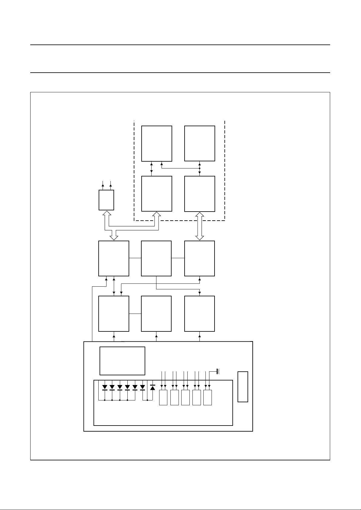
APPLICATION INFORMATION
HOST
INTERFACE
AUDIO
LEFT
RIGHT
DAC
S
2
I
CD-ROM
SCSI
DECODER
BUFFER
MANAGEMENT
DATA
SYSTEM
CONTROLLER
B
2
S
OQ8868
MGE337
DATA PATH
andbook, full pagewidth
DECODER
DIGITAL
HF
D1D2D3D4D5
DD
V
MECHANISM
CD65
LO9585
DSICS
OQ8868
SERVO IC
OSDALAS2
AMPLIFIER
DIGITAL
OQ8875
LASER
MOTOR
CONTROL
DSD3
POWER
AMPLIFIER
FOCUS
A
MONITOR
SZA1010
TRACKING
B
SYSTEM
CONTROLLER
POWER
ANALOG
MOTOR
SLED
D
C
SERVO
LO9585
TDA7072A
AMPLIFIER
HOME
SWITCH
E
2-STAGE,
A = FOCUS ACTUATOR
B = RADIAL ACTUATOR
C = SLED MOTOR
D = SPINDLE MOTOR
E = HOME SWITCH
LOADER
3-SPOTS
CD-MECHANISM
Fig.4 Application diagram.
1997 Feb 12 16
Page 17
Philips Semiconductors Product specification
Digital Servo Integrated Circuit Silent
(DSICS)
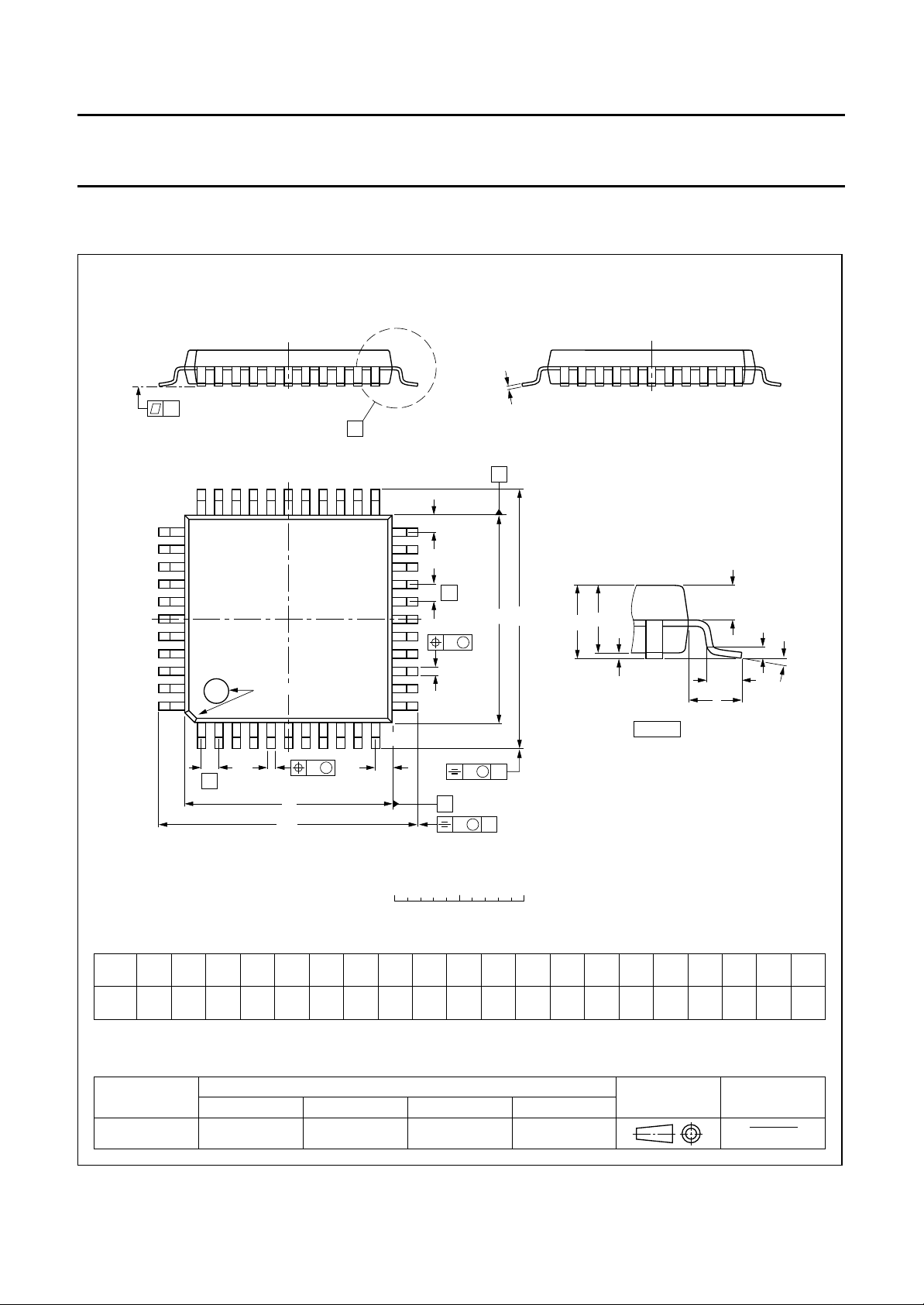
PACKAGE OUTLINE
QFP44: plastic quad flat package; 44 leads (lead length 1.3 mm); body 10 x 10 x 1.75 mm
c
y
X
A
33 23
34
22
Z
E
OQ8868
SOT307-2
e
w M
b
p
pin 1 index
44
1
w M
b
0.25
p
D
H
D
cE
p
0.40
0.25
0.20
0.14
D
10.1
9.9
e
DIMENSIONS (mm are the original dimensions)
mm
A
max.
2.10
0.25
0.05
1.85
1.65
UNIT A1A2A3b
Note
1. Plastic or metal protrusions of 0.25 mm maximum per side are not included.
12
11
Z
D
B
v M
0 2.5 5 mm
scale
(1)
(1) (1)(1)
eH
H
10.1
9.9
12.9
0.8 1.3
12.3
v M
D
H
E
E
A
B
LLpQZywv θ
E
12.9
12.3
0.95
0.55
A
2
A
A
1
detail X
0.85
0.75
0.15 0.10.15
Q
(A )
3
θ
L
p
L
Z
E
D
1.2
0.8
1.2
0.8
o
10
o
0
OUTLINE
VERSION
SOT307-2
IEC JEDEC EIAJ
REFERENCES
1997 Feb 12 17
EUROPEAN
PROJECTION
ISSUE DATE
92-11-17
95-02-04
Page 18

Philips Semiconductors Product specification
Digital Servo Integrated Circuit Silent
(DSICS)
SOLDERING
Introduction
There is no soldering method that is ideal for all IC
packages. Wave soldering is often preferred when
through-hole and surface mounted components are mixed
on one printed-circuit board. However, wave soldering is
not always suitable for surface mounted ICs, or for
printed-circuits with high population densities. In these
situations reflow soldering is often used.
This text gives a very brief insight to a complex technology.
A more in-depth account of soldering ICs can be found in
our
“IC Package Databook”
Reflow soldering
Reflow soldering techniques are suitable for all QFP
packages.
The choice of heating method may be influenced by larger
plastic QFP packages (44 leads, or more). If infrared or
vapour phase heating is used and the large packages are
not absolutely dry (less than 0.1% moisture content by
weight), vaporization of the small amount of moisture in
them can cause cracking of the plastic body. For more
information, refer to the Drypack chapter in our
Reference Handbook”
Reflow soldering requires solder paste (a suspension of
fine solder particles, flux and binding agent) to be applied
to the printed-circuit board by screen printing, stencilling or
pressure-syringe dispensing before package placement.
Several techniques exist for reflowing; for example,
thermal conduction by heated belt. Dwell times vary
between 50 and 300 seconds depending on heating
method. Typical reflow temperatures range from
215 to 250 °C.
Preheating is necessary to dry the paste and evaporate
the binding agent. Preheating duration: 45 minutes at
45 °C.
(order code 9398 652 90011).
“Quality
(order code 9397 750 00192).
OQ8868
Wave soldering
Wave soldering is not recommended for QFP packages.
This is because of the likelihood of solder bridging due to
closely-spaced leads and the possibility of incomplete
solder penetration in multi-lead devices.
If wave soldering cannot be avoided, the following
conditions must be observed:
• A double-wave (a turbulent wave with high upward
pressure followed by a smooth laminar wave)
soldering technique should be used.
• The footprint must be at an angle of 45° to the board
direction and must incorporate solder thieves
downstream and at the side corners.
Even with these conditions, do not consider wave
soldering the following packages: QFP52 (SOT379-1),
QFP100 (SOT317-1), QFP100 (SOT317-2),
QFP100 (SOT382-1) or QFP160 (SOT322-1).
During placement and before soldering, the package must
be fixed with a droplet of adhesive. The adhesive can be
applied by screen printing, pin transfer or syringe
dispensing. The package can be soldered after the
adhesive is cured.
Maximum permissible solder temperature is 260 °C, and
maximum duration of package immersion in solder is
10 seconds, if cooled to less than 150 °C within
6 seconds. Typical dwell time is 4 seconds at 250 °C.
A mildly-activated flux will eliminate the need for removal
of corrosive residues in most applications.
Repairing soldered joints
Fix the component by first soldering two diagonallyopposite end leads. Use only a low voltage soldering iron
(less than 24 V) applied to the flat part of the lead. Contact
time must be limited to 10 seconds at up to 300 °C. When
using a dedicated tool, all other leads can be soldered in
one operation within 2 to 5 seconds between
270 and 320 °C.
1997 Feb 12 18
Page 19

Philips Semiconductors Product specification
Digital Servo Integrated Circuit Silent
OQ8868
(DSICS)
DEFINITIONS
Data sheet status
Objective specification This data sheet contains target or goal specifications for product development.
Preliminary specification This data sheet contains preliminary data; supplementary data may be published later.
Product specification This data sheet contains final product specifications.
Limiting values
Limiting values given are in accordance with the Absolute Maximum Rating System (IEC 134). Stress above one or
more of the limiting values may cause permanent damage to the device. These are stress ratings only and operation
of the device at these or at any other conditions above those given in the Characteristics sections of the specification
is not implied. Exposure to limiting values for extended periods may affect device reliability.
Application information
Where application information is given, it is advisory and does not form part of the specification.
LIFE SUPPORT APPLICATIONS
These products are not designed for use in life support appliances, devices, or systems where malfunction of these
products can reasonably be expected to result in personal injury. Philips customers using or selling these products for
use in such applications do so at their own risk and agree to fully indemnify Philips for any damages resulting from such
improper use or sale.
PURCHASE OF PHILIPS I
Purchase of Philips I
components in the I2C system provided the system conforms to the I2C specification defined by
Philips. This specification can be ordered using the code 9398 393 40011.
2
C COMPONENTS
2
C components conveys a license under the Philips’ I2C patent to use the
1997 Feb 12 19
Page 20

Philips Semiconductors – a worldwide company
Argentina: see South America
Australia: 34 Waterloo Road, NORTH RYDE, NSW 2113,
Tel. +61 2 9805 4455, Fax.+61 29805 4466
Austria: Computerstr. 6, A-1101 WIEN, P.O. Box 213,
Tel. +43 1 60 101, Fax.+43 160 1011210
Belarus: Hotel Minsk Business Center, Bld. 3, r. 1211, Volodarski Str.6,
220050 MINSK, Tel. +375 172 200 733,Fax. +375172 200773
Belgium: see The Netherlands
Brazil: see South America
Bulgaria: Philips Bulgaria Ltd., Energoproject, 15th floor,
51 James Bourchier Blvd., 1407 SOFIA,
Tel. +359 2 689 211, Fax.+359 2689 102
Canada: PHILIPS SEMICONDUCTORS/COMPONENTS,
Tel. +1 800 234 7381
China/Hong Kong: 501 Hong Kong Industrial Technology Centre,
72 Tat Chee Avenue, Kowloon Tong, HONG KONG,
Tel. +852 2319 7888, Fax. +8522319 7700
Colombia: see South America
Czech Republic: see Austria
Denmark: Prags Boulevard 80, PB 1919, DK-2300 COPENHAGEN S,
Tel. +45 32 88 2636, Fax.+45 3157 1949
Finland: Sinikalliontie 3, FIN-02630 ESPOO,
Tel. +358 9 615800, Fax. +3589 61580/xxx
France: 4 Rue du Port-aux-Vins, BP317, 92156 SURESNES Cedex,
Tel. +33 1 40 99 6161, Fax. +331 4099 6427
Germany: Hammerbrookstraße 69, D-20097 HAMBURG,
Tel. +49 40 23 53 60,Fax. +4940 23536 300
Greece: No. 15, 25th March Street, GR 17778TAVROS/ATHENS,
Tel. +30 1 4894 339/239, Fax.+30 14814 240
Hungary: see Austria
India: Philips INDIA Ltd, Shivsagar Estate, A Block, Dr. Annie Besant Rd.
Worli, MUMBAI 400 018, Tel. +91 22 4938541, Fax.+91 224938 722
Indonesia: see Singapore
Ireland: Newstead, Clonskeagh, DUBLIN 14,
Tel. +353 1 7640 000, Fax.+353 17640 200
Israel: RAPAC Electronics, 7 Kehilat Saloniki St, TEL AVIV61180,
Tel. +972 3 645 0444, Fax.+972 3649 1007
Italy: PHILIPS SEMICONDUCTORS, Piazza IV Novembre 3,
20124 MILANO, Tel. +39 2 6752 2531,Fax. +392 67522557
Japan: Philips Bldg 13-37, Kohnan 2-chome, Minato-ku, TOKYO 108,
Tel. +81 3 3740 5130, Fax.+81 33740 5077
Korea: Philips House, 260-199 Itaewon-dong, Yongsan-ku, SEOUL,
Tel. +82 2 709 1412, Fax.+82 2709 1415
Malaysia: No. 76 Jalan Universiti, 46200 PETALING JAYA, SELANGOR,
Tel. +60 3 750 5214, Fax. +603 7574880
Mexico: 5900 Gateway East, Suite 200, EL PASO, TEXAS 79905,
Tel. +9-5 800 234 7381
Middle East: see Italy
Netherlands: Postbus 90050, 5600 PB EINDHOVEN, Bldg. VB,
Tel. +31 40 27 82785, Fax.+31 4027 88399
New Zealand: 2 Wagener Place, C.P.O. Box 1041, AUCKLAND,
Tel. +64 9 849 4160, Fax.+64 9849 7811
Norway: Box 1, Manglerud 0612, OSLO,
Tel. +47 22 74 8000, Fax.+47 2274 8341
Philippines: Philips Semiconductors Philippines Inc.,
106 Valero St. Salcedo Village, P.O. Box2108 MCC,MAKATI,
Metro MANILA, Tel. +63 2 816 6380,Fax. +632 8173474
Poland: Ul. Lukiska 10, PL 04-123 WARSZAWA,
Tel. +48 22 612 2831, Fax.+48 22612 2327
Portugal: see Spain
Romania: see Italy
Russia: Philips Russia, Ul. Usatcheva 35A, 119048 MOSCOW,
Tel. +7 095 755 6918, Fax.+7 095755 6919
Singapore: Lorong 1, Toa Payoh, SINGAPORE 1231,
Tel. +65 350 2538, Fax. +65251 6500
Slovakia: see Austria
Slovenia: see Italy
South Africa: S.A. PHILIPS Pty Ltd., 195-215 Main Road Martindale,
2092 JOHANNESBURG, P.O. Box 7430 Johannesburg 2000,
Tel. +27 11 470 5911, Fax.+27 11470 5494
South America: Rua do Rocio 220, 5th floor, Suite 51,
04552-903 São Paulo, SÃO PAULO - SP, Brazil,
Tel. +55 11 821 2333, Fax.+55 11829 1849
Spain: Balmes 22, 08007 BARCELONA,
Tel. +34 3 301 6312, Fax.+34 3301 4107
Sweden: Kottbygatan 7, Akalla, S-16485 STOCKHOLM,
Tel. +46 8 632 2000, Fax.+46 8632 2745
Switzerland: Allmendstrasse 140, CH-8027 ZÜRICH,
Tel. +41 1 488 2686, Fax.+41 1481 7730
Taiwan: Philips Semiconductors, 6F, No. 96, Chien Kuo N. Rd., Sec.1,
TAIPEI, Taiwan Tel. +886 2 2134 2870, Fax.+886 22134 2874
Thailand: PHILIPS ELECTRONICS (THAILAND) Ltd.,
209/2 Sanpavuth-Bangna Road Prakanong, BANGKOK 10260,
Tel. +66 2 745 4090, Fax.+66 2398 0793
Turkey: Talatpasa Cad. No. 5, 80640 GÜLTEPE/ISTANBUL,
Tel. +90 212 279 2770, Fax.+90 212282 6707
Ukraine: PHILIPS UKRAINE, 4 Patrice Lumumba str., Building B, Floor 7,
252042 KIEV, Tel. +380 44 264 2776, Fax. +38044 2680461
United Kingdom: Philips Semiconductors Ltd., 276 Bath Road, Hayes,
MIDDLESEX UB3 5BX, Tel. +44 181 7305000, Fax.+44 181754 8421
United States: 811 East Arques Avenue, SUNNYVALE, CA 94088-3409,
Tel. +1 800 234 7381
Uruguay: see South America
Vietnam: see Singapore
Yugoslavia: PHILIPS, Trg N. Pasica 5/v, 11000 BEOGRAD,
Tel. +381 11 625 344, Fax.+38111 635777
For all other countries apply to: Philips Semiconductors, Marketing & Sales Communications,
Building BE-p, P.O. Box 218, 5600 MD EINDHOVEN, TheNetherlands, Fax.+31 4027 24825
© Philips Electronics N.V. 1997 SCA53
All rights are reserved. Reproduction in whole or in part is prohibited without the prior written consent of the copyright owner.
The information presented in this document does not form part of any quotation or contract, is believed to be accurate and reliable and may be changed
without notice. No liability will be accepted by the publisher for any consequence of its use. Publication thereof does not convey nor imply any license
under patent- or other industrial or intellectual property rights.
Internet: http://www.semiconductors.philips.com
Printed in The Netherlands 547027/00/02/pp20 Date of release: 1997 Feb12 Document order number: 9397 75001655
 Loading...