

Page 1
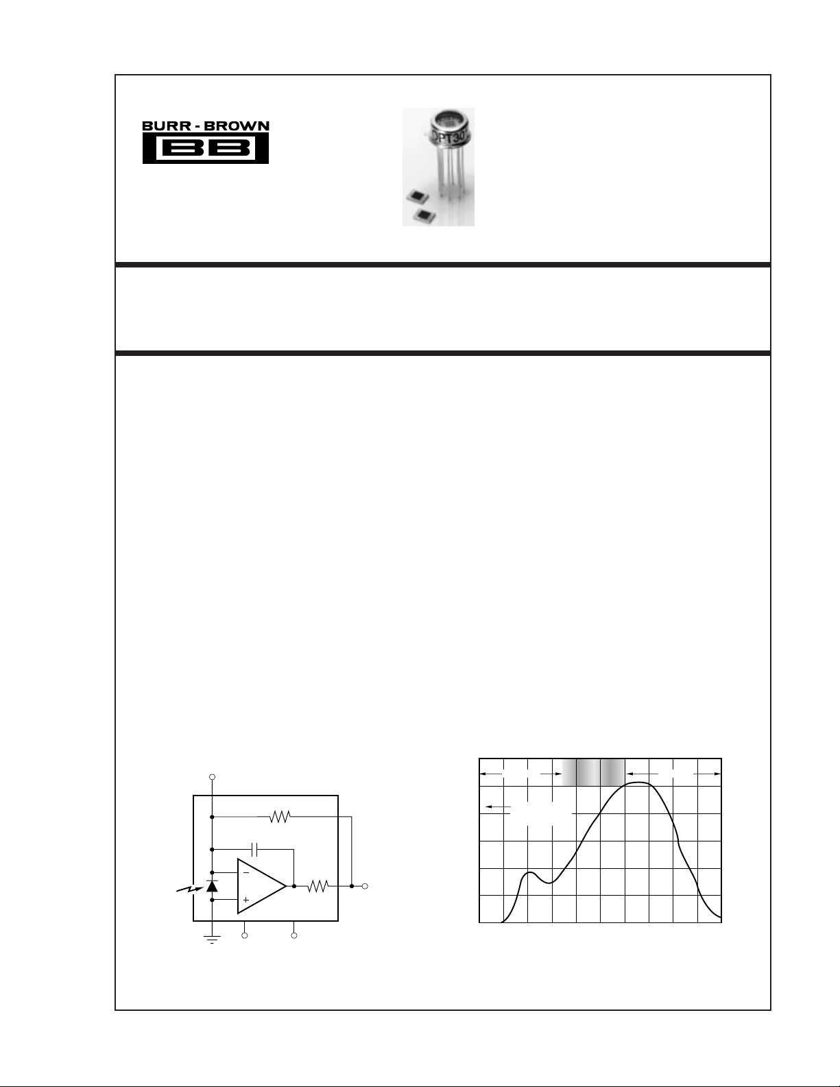
®
FPO
70%
INTEGRATED PHOTODIODE
AND AMPLIFIER
OPT301
FEATURES
● PHOTODIODE SIZE: 0.090 x 0.090 inch
(2.29 x 2.29mm)
● 1MΩ FEEDBACK RESISTOR
● HIGH RESPONSIVITY: 0.47A/W
(650nm)
● IMPROVED UV RESPONSE
● LOW DARK ERRORS: 2mV
● BANDWIDTH: 4kHz
● WIDE SUPPLY RANGE:
±2.25 to ±18V
● LOW QUIESCENT CURRENT: 400µA
● HERMETIC TO-99
APPLICATIONS
● MEDICAL INSTRUMENTATION
● LABORATORY INSTRUMENTATION
● POSITION AND PROXIMITY SENSORS
● PHOTOGRAPHIC ANALYZERS
● SMOKE DETECTORS
2
1MΩ
40pF
4
DESCRIPTION
The OPT301 is an opto-electronic integrated circuit
containing a photodiode and transimpedance
amplifier on a single dielectrically isolated chip. The
transimpedance amplifier consists of a precision FETinput op amp and an on-chip metal film resistor. The
0.09 x 0.09 inch photodiode is operated at zero bias for
excellent linearity and low dark current.
The integrated combination of photodiode and
transimpedance amplifier on a single chip eliminates
the problems commonly encountered in discrete designs such as leakage current errors, noise pick-up and
gain peaking due to stray capacitance.
The OPT301 operates over a wide supply range (±2.25
to ±18V) and supply current is only 400µA. It is
packaged in a hermetic TO-99 metal package with a
glass window, and is specified for the –40°C to 85°C
temperature range.
SPECTRAL RESPONSIVITY
0.5
0.4
0.3
Ultraviolet
Using Internal
1MΩ Resistor
Blue
Green
Yellow
Red
Infrared
0.5
0.4
0.3
75Ω
5
V
λ
OPT301
1
83
V+
International Airport Industrial Park • Mailing Address: PO Box 11400, Tucson, AZ 85734 • Street Address: 6730 S. Tucson Blvd., Tucson, AZ 85706 • Tel: (520) 746-1111 • Twx: 910-952-1111
Internet: http://www.burr-brown.com/ • FAXLine: (800) 548-6133 (US/Canada Only) • Cable: BBRCORP • Telex: 066-6491 • FAX: (520) 889-1510 • Immediate Product Info: (800) 548-6132
©
1994 Burr-Brown Corporation PDS-1228B Printed in U.S.A. January, 1994
V–
O
0.2
Voltage Output (V/µW)
0.1
0
100 200 300 400 500 600 700 800 900 1000 1100
Wavelength (nm)
0.2
0.1
Photodiode Responsivity (A/W)
0
Page 2

SPECIFICATIONS
ELECTRICAL
At TA = +25°C, VS = ±15V, λ = 650nm, internal 1MΩ feedback resistor, unless otherwise noted.
OPT301M
PARAMETER CONDITIONS MIN TYP MAX UNITS
RESPONSIVITY
Photodiode Current 650nm 0.47 A/W
Voltage Output 650nm 0.47 V/µW
vs Temperature 200 ppm/°C
Unit-to-Unit Variation 650nm ±5%
Nonlinearity
Photodiode Area (0.090 x 0.090in) 0.008 in
DARK ERRORS, RTO
Offset Voltage, Output ±0.5 ±2mV
vs Temperature ±10 µV/°C
vs Power Supply V
Voltage Noise Measured BW = 0.1 to 100kHz 160 µVrms
RESISTOR—1MΩ Internal
Resistance 1MΩ
Tolerance ±0.5 ±2%
vs Temperature 50 ppm/°C
FREQUENCY RESPONSE
Bandwidth, Large or Small-Signal, –3dB 4 kHz
Rise Time, 10% to 90% 90 µs
Settling Time, 1% FS to Dark 240 µs
Overload Recovery Time 100% overdrive, V
OUTPUT
Voltage Output R
Capacitive Load, Stable Operation 10 nF
Short-Circuit Current ±18 mA
POWER SUPPLY
Specified Operating Voltage ±15 V
Operating Voltage Range ±2.25 ±18 V
Quiescent Current I
TEMPERATURE RANGE
Specification –40 +85 °C
Operating/Storage –55 +125 °C
Thermal Resistance,
NOTES: (1) Deviation in percent of full scale from best-fit straight line. (2) Referred to Output. Includes all error sources.
(1)
FS Output = 10V 0.01 % of FS
(2.29 x 2.29mm) 5.2 mm
(2)
= ±2.25V to ±18V 10 100 µV/V
S
0.1% FS to Dark 350 µs
0.01% FS to Dark 900 µs
= ±15V 240 µs
100% overdrive, V
100% overdrive, V
θ
JA
S
= ±5V 500 µs
S
= ±2.25V 1000 µs
S
= 10kΩ (V+) – 1.25 (V+) – 0.65 V
L
R
= 5kΩ (V+) – 2 (V+) – 1 V
L
= 0 ±0.4 ±0.5 mA
O
200 °C/W
2
2
PHOTODIODE SPECIFICATIONS
At TA = +25°C, unless otherwise noted.
Photodiode of OPT301
PARAMETER CONDITIONS MIN TYP MAX UNITS
Photodiode Area (0.090 x 0.090in) 0.008 in
Current Responsivity 650nm 0.47 A/W
Dark Current V
vs Temperature doubles every 10°C
Capacitance V
NOTE: (1) Voltage Across Photodiode.
®
OPT301
(2.29 x 2.29mm) 5.1 mm
(1)
= 0V
D
= 0V
D
(1)
500 fA
4000 pF
2
2
2
Page 3

SPECIFICATIONS (CONT)
ELECTRICAL Op Amp Section of OPT301
At TA = +25°C, VS = ±15V, unless otherwise noted.
OPT301 Op Amp
PARAMETER CONDITIONS MIN TYP MAX UNITS
INPUT
Offset Voltage ±0.5 mV
vs Temperature ±5 µV/°C
vs Power Supply V
Input Bias Current 1pA
vs Temperature doubles every 10°C
NOISE
Input Voltage Noise
Voltage Noise Density, f=10Hz 30 nV/√Hz
f=100Hz 25 nV/√Hz
f=1kHz 15 nV/√Hz
Current Noise Density, f=1kHz 0.8 fA/√Hz
INPUT VOLTAGE RANGE
Common-Mode Input Range ±14.4 V
Common-Mode Rejection 106 dB
INPUT IMPEDANCE
Differential 10
Common-Mode 10
OPEN-LOOP GAIN
Open-Loop Voltage Gain 120 dB
FREQUENCY RESPONSE
Gain-Bandwidth Product 380 kHz
Slew Rate 0.5 V/µs
Settling Time 0.1% 4 µs
0.01% 5 µs
OUTPUT
Voltage Output R
Short-Circuit Current ±18 mA
POWER SUPPLY
Specified Operating Voltage ±15 V
Operating Voltage Range ±2.25 ±18 V
Quiescent Current I
NOTE: (1) Op amp specifications provided for information and comparison only.
= ±2.25V to ±18V 10 µV/V
S
12
||3 Ω||pF
12
||3 Ω||pF
= 10kΩ (V+) – 1.25 (V+) – 0.65 V
L
R
= 5kΩ (V+) – 2 (V+) – 1 V
L
= 0 ±0.4 ±0.5 mA
O
(1)
6
The information provided herein is believed to be reliable; however, BURR-BROWN assumes no responsibility for inaccuracies or omissions. BURR-BROWN assumes
no responsibility for the use of this information, and all use of such information shall be entirely at the user’s own risk. Prices and specifications are subject to change
without notice. No patent rights or licenses to any of the circuits described herein are implied or granted to any third party. BURR-BROWN does not authorize or warrant
any BURR-BROWN product for use in life support devices and/or systems.
3
OPT301
®
Page 4
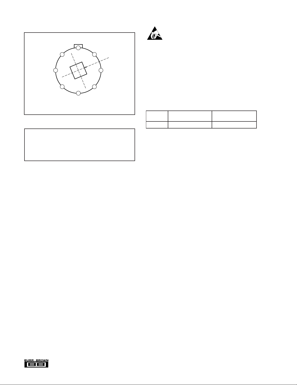
PIN CONFIGURATION
Top View
V+
26
V–
NOTE: Metal package is internally connected to common (Pin 8).
Common
8
1
3
4
1MΩ Feedback
NC
7
5
Output
Photodiode
Area
NC–In
ABSOLUTE MAXIMUM RATINGS
Supply Voltage................................................................................... ±18V
Input Voltage Range (Common Pin) .................................................... ±V
Output Short-Circuit (to ground)............................................... Continuous
Operating Temperature................................................... –55°C to +125°C
Storage Temperature...................................................... –55°C to +125°C
Junction Temperature .................................................................... +125°C
Lead Temperature (soldering, 10s)................................................ +300°C
ELECTROSTATIC
DISCHARGE SENSITIVITY
This integrated circuit can be damaged by ESD. Burr-Brown
recommends that all integrated circuits be handled with appropriate precautions. Failure to observe proper handling and
installation procedures can cause damage.
ESD damage can range from subtle performance degradation
to complete device failure. Precision integrated circuits may
be more susceptible to damage because very small parametric
changes could cause the device not to meet its published
specifications.
PACKAGE INFORMATION
PRODUCT PACKAGE NUMBER
OPT301M 8-Pin TO-99 001-1
NOTE: (1) For detailed drawing and dimension table, please see end of data
S
sheet, or Appendix C of Burr-Brown IC Data Book.
PACKAGE DRAWING
(1)
®
OPT301
4
Page 5

TYPICAL PERFORMANCE CURVES
At TA = +25°C, VS = ±15V, λ = 650nm, unless otherwise noted.
1.0
NORMALIZED SPECTRAL RESPONSIVITY
0.8
650nm
(0.52A/W)
(0.47A/W)
0.6
0.4
0.2
Normalized Current or Voltage Output
0
100 200 300 400 500 600 700 800 900 1000 1100
Wavelength (nm)
VOLTAGE RESPONSIVITY vs IRRADIANCE
10
1
= 10MΩ
F
0.1
Output Voltage (V)
0.01
R
= 1MΩ
F
R
= 100kΩ
F
R
F
R
= 10kΩ
λ = 650nm
0.001
0.001 0.01 1 10 1000.1
Irradiance (W/m
2
)
VOLTAGE RESPONSIVITY vs RADIANT POWER
10
1
= 10MΩ
F
R
0.1
Output Voltage (V)
0.01
0.001
0.01 0.1 10 100 1k1
VOLTAGE OUTPUT RESPONSIVITY vs FREQUENCY
10
1
0.1
Responsivity (V/µW)
0.01
RF = 33kΩ C
RF = 10kΩ C
0.001
100
= 1MΩ
F
R
= 100kΩ
F
R
= 10kΩ
F
R
λ = 650nm
Radiant Power (µW)
RF = 10MΩ
RF = 3.3MΩ
λ = 650nm
RF = 1MΩ
EXT
EXT
RF = 330kΩ C
RF = 100kΩ C
= 180pF
= 350pF
EXT
= 30pF
= 90pF
EXT
1k 10k 100k 1M
Frequency (Hz)
6
60
50
40
30
Units (%)
20
10
0
0.45
DISTRIBUTION OF RESPONSIVITY
λ = 650nm
Distribution Totals
100%
Laboratory Test
Data
0.46 0.47 0.48 0.49 0.5
Responsivity (A/W)
1.0
0.8
0.6
0.4
Relative Response
0.2
0
5
RESPONSE vs INCIDENT ANGLE
1.0
θ
0.8
0.6
0.4
0.2
0
0
±20 ±40 ±60 ±80
Incident Angle (°)
®
OPT301
Page 6

TYPICAL PERFORMANCE CURVES
At TA = +25°C, VS = ±15V, λ = 650nm, unless otherwise noted.
0.6
0.5
0.4
0.3
0.2
Quiescent Current (mA)
0.1
0
QUIESCENT CURRENT vs TEMPERATURE
VS = ±15V
VS = ±2.25V
–50 –25 0 25 50 75 100 125
–75
Temperature (°C)
Dice
1000
vs MEASUREMENT BANDWIDTH
Dotted lines show
noise beyond the
signal bandwidth.
100
10
Noise Voltage (µVrms)
0.1
1
RF = 100kΩ C
= 100MΩ
F
R
1 10 1k 10k 100k100
OUTPUT NOISE VOLTAGE
= 1MΩ
F
= 10MΩ
F
R
R
RF = 10kΩ C
= 90pF
EXT
Measurement Bandwidth (Hz)
EXT
= 350pF
SMALL-SIGNAL DYNAMIC RESPONSE
20mV/div
100µs/div
NOISE EFFECTIVE POWER
–7
10
vs MEASUREMENT BANDWIDTH
Dotted lines indicate
noise measured beyond
–8
10
the signal bandwidth.
λ = 650nm
–9
10
–10
10
–11
10
Noise Effective Power (W)
–12
10
LARGE-SIGNAL DYNAMIC RESPONSE
2V/div
100µs/div
= 10k
R
F
R
= 100k
F
= 1M
R
F
= 10M
R
F
RF = 100M
®
OPT301
–13
10
–14
10
1 10 1k 10k 100k100
Measurement Bandwidth (Hz)
6
Page 7

APPLICATIONS INFORMATION
Figure 1 shows the basic connections required to operate the
OPT301. Applications with high-impedance power supplies
may require decoupling capacitors located close to the
device pins as shown. Output is zero volts with no light and
increases with increasing illumination.
2
1MΩ
R
F
4
I
ID is proportional
to light intensity
(radiant power).
(0V)
I
D
40pF
λ
1
83
NOTE: Metal package
is internally connected
to common (Pin 8).
FIGURE 1. Basic Circuit Connections.
Photodiode current, I
D
or flux (in watts) falling on the photodiode. At a wavelength
of 650nm (visible red) the photodiode Responsivity, RI, is
approximately 0.45A/W. Responsivity at other wavelengths
is shown in the typical performance curve “Responsivity vs
Wavelength.”
The typical performance curve “Output Voltage vs Radiant
Power” shows the response throughout a wide range of
radiant power. The response curve “Output Voltage vs
Irradiance” is based on the photodiode area of 5.23 x 10
The OPT301’s voltage output is the product of the photodiode
current times the feedback resistor, (I
feedback resistor is laser trimmed to 1MΩ ±2%. Using this
resistor, the output voltage responsivity, RV, is approximately
0.45V/µW at 650nm wavelength.
An external resistor can be used to set a different voltage
responsivity. For values of R
capacitor, C
, should be connected in parallel with RF (see
EXT
Figure 2). This capacitor eliminates gain peaking and prevents
instability. The value of C
Figure 2.
LIGHT SOURCE POSITIONING
The OPT301 is 100% tested with a light source that uniformly
illuminates the full area of the integrated circuit, including
the op amp. Although all IC amplifiers are light-sensitive to
some degree, the OPT301 op amp circuitry is designed to
minimize this effect. Sensitive junctions are shielded with
metal, and differential stages are cross-coupled. Furthermore,
the photodiode area is very large relative to the op amp input
circuitry making these effects negligible.
0.1µF 0.1µF
, is proportional to the radiant power
less than 1MΩ, an external
F
can be read from the table in
EXT
D
75Ω
OPT301
–15V+15V
DRF
5
V
O
VO = ID R
–6m2
). The internal
If your light source is focused to a small area, be sure that
it is properly aimed to fall on the photodiode. If a narrowly
focused light source were to miss the photodiode area and
fall only on the op amp circuitry, the OPT301 would not
perform properly. The large (0.090 x 0.090 inch) photodiode
area allows easy positioning of narrowly focused light
sources. The photodiode area is easily visible—it appears
very dark compared to the surrounding active circuitry.
The incident angle of the light source also affects the
apparent sensitivity in uniform irradiance. For small incident
angles, the loss in sensitivity is simply due to the smaller
effective light gathering area of the photodiode (proportional
to the cosine of the angle). At a greater incident angle, light
is reflected and scattered by the side of the package. These
effects are shown in the typical performance curve
“Response vs Incident Angle.”
F
DARK ERRORS
The dark errors in the specification table include all sources.
The dominant error source is the input offset voltage of the
op amp. Photodiode dark current and input bias current of
the op amp are approximately 2pA and contribute virtually
no offset error at room temperature. Dark current and input
bias current double for each 10°C above 25°C. At 70°C, the
error current can be approximately 100pA. This would
produce a 1mV offset with R
= 10MΩ. The OPT301 is
F
useful with feedback resistors of 100MΩ or greater at room
temperature. The dark output voltage can be trimmed to
zero with the optional circuit shown in Figure 3.
C
EXT
R
.
2
1MΩ
40pF
F
4
75Ω
5
λ
OPT301
1
83
V+
EXTERNAL R
100MΩ
10MΩ
1MΩ
330kΩ 30pF
100kΩ 130pF
33kΩ 180pF
10kΩ 350pF
NOTE: (1) No C
FIGURE 2. Using External Feedback Resistor.
V–
F
required.
EXT
C
EXT
(1)
(1)
(1)
V
= ID R
O
F
6
®
7
OPT301
Page 8

When used with very large feedback resistors, tiny leakage
currents on the circuit board can degrade the performance of
the OPT301. Careful circuit board design and clean assembly
procedures will help achieve best performance. A “guard
trace” on the circuit board can help minimize leakage to the
critical non-inverting input (pin 2). This guard ring should
encircle pin 2 and connect to Common, pin 8.
DYNAMIC RESPONSE
Using the internal 1MΩ resistor, the dynamic response of
the photodiode/op amp combination can be modeled as a
simple R/C circuit with a –3dB cutoff frequency of 4kHz.
This yields a rise time of approximately 90µs (10% to 90%).
Dynamic response is not limited by op amp slew rate. This
is demonstrated by the dynamic response oscilloscope
photographs showing virtually identical large-signal and
small-signal response.
Dynamic response will vary with feedback resistor value as
shown in the typical performance curve “Voltage Output
Responsivity vs Frequency.” Rise time (10% to 90%) will
vary according to the –3dB bandwidth produced by a given
feedback resistor value—
0.35
tR≈
f
C
(1)
where:
t
is the rise time (10% to 90%)
R
is the –3dB bandwidth
f
C
LINEARITY PERFORMANCE
Current output of the photodiode is very linear with radiant
power throughout a wide range. Nonlinearity remains below
approximately 0.02% up to 100µA photodiode current. The
photodiode can produce output currents of 1mA or greater
with high radiant power, but nonlinearity increases to several
percent in this region.
This excellent linearity at high radiant power assumes that
the full photodiode area is uniformly illuminated. If the light
source is focused to a small area of the photodiode,
nonlinearity will occur at lower radiant power.
NOISE PERFORMANCE
Noise performance of the OPT301 is determined by the op
amp characteristics in conjunction with the feedback
components and photodiode capacitance. The typical
performance curve “Output Noise Voltage vs Measurement
Bandwidth” shows how the noise varies with R
and measured
F
bandwidth (1Hz to the indicated frequency). The signal
bandwidth of the OPT301 is indicated on the curves. Noise
can be reduced by filtering the output with a cutoff frequency
equal to the signal bandwidth.
Output noise increases in proportion to the square-root of the
feedback resistance, while responsivity increases linearly
with feedback resistance. So best signal-to-noise ratio is
achieved with large feedback resistance. This comes with
the trade-off of decreased bandwidth.
The noise performance of a photodetector is sometimes
characterized by Noise Effective Power (NEP). This is the
radiant power which would produce an output signal equal
to the noise level. NEP has the units of radiant power
(watts). The typical performance curve “Noise Effective
Power vs Measurement Bandwidth” shows how NEP varies
and measurement bandwidth.
with R
F
2
100µA
1/2 REF200
100Ω
100Ω
100µA
1/2 REF200
V+
V–
λ
83
500Ω
0.01µF
Adjust dark output for 0V.
Trim Range: ±7mV
1MΩ
40pF
1
V+
V–
75Ω
OPT301
4
5
FIGURE 3. Dark Error (Offset) Adjustment Circuit.
®
OPT301
V
O
λ
FIGURE 4. Responsivity (Gain) Adjustment Circuit.
8
2
1MΩ
R
F
4
40pF
75Ω
OPT301
1
83
V+
V–
Gain Adjustment
5
+50%; –0%
5kΩ
10kΩ
V
O
Page 9

2
1MΩ
R
F
4
40pF
75Ω
5
λ
OPT301
1
83
V+
Advantages: High gain with low resistor values.
Less sensitive to circuit board leakage.
Disadvantage: Higher offset and noise than by using high
value for R
V–
.
F
R1 + R
V
= ID R
O
R
R
1
19kΩ
R
2
1kΩ
This OPT301 used
as photodiode, only.
2
1MΩ
R
F
4
NC
2
F
2
λ
I
D1
40pF
75Ω
5
NC
OPT301
1
83
8
2
1MΩ
R
F
4
40pF
FIGURE 5. “T” Feedback Network.
2
1MΩ
R
F1
4
40pF
75Ω
5
λ
Max linear
input voltage
(V+) –0.6V typ
λ
OPT301
1
83
V+
2
40pF
83
V+
V–
1MΩ
R
F2
75Ω
OPT301
1
V–
= I
V
O
D1 RF1
4
5
V
O
FIGURE 6. Summing Output of Two OPT301s.
= I
+ I
D2 RF2
D2 RF2
75Ω
5
λ
OPT301
1
83
I
D2
V+
V–
FIGURE 7. Differential Light Measurement.
2
1MΩ
40pF
VO = (I
Bandwidth is reduced to
2.8kHz due to additional
photodiode capacitance.
R
F
4
75Ω
5
λ
OPT301
1
83
I
D
+15V
FIGURE 8. Current Output Circuit.
–15V
IO = ID 1 +
R
F
R
1
V
O
D2 – ID1) RF
R
1
1kΩ
IO ≤ 5mA
6
®
9
OPT301
Page 10

2
1MΩ
R
F
4
40pF
75Ω
5
λ
OPT301
1
83
(1)
V
Z
3.3V
FIGURE 9. Single Power Supply Operation.
5kΩ
0.1µF
V+
NOTE: (1) Zener diode or other shunt regulator.
+
= IDR
V
O
F
–
V
Z
(pesudo-ground)
2
1MΩ
R
F1
4
Output filter reduces
40pF
75Ω
output noise from
250µV to 195µV.
5
λ
OPT301
8
1
V+
3
V–
FIGURE 10. Output Filter to Reduce Noise.
10nF
V
O
2
1MΩ
R
F1
4
40pF
75Ω
5
λ
OPT301
1
8
83
1MΩ
V–
R
F2
75Ω
4
5
V+
2
40pF
λ
OPT301
1
83
V+
V–
= I
V
O1
D1 RF1
= I
V
O2
D2 RF2
2
3
100kΩ
100kΩ
10kΩ
10kΩ
G = 10
1
14
100kΩ
100kΩ
LOG100
INA106
C
C
5
Difference Measurement
V
O
6
1
7
10
3
1nF
= 10 (V
Log of Ratio Measurement
– VO1)
O2
(Absorbance)
= K log
V
O
V
V
O1
O2
FIGURE 11. Differential Light Measurement.
®
OPT301
10
Page 11

C
2
R
3
100kΩ
2
1MΩ
0.1µF
A
1
R
1
4
1MΩ
C
0.1µF
R
2
1MΩ
1
40pF
75Ω
5
λ
OPT301
8
V
FIGURE 12. DC Restoration Rejects Unwanted Steady-State Background Light.
1/2
REF200
100µA
2
40pF
1MΩ
1
4
75Ω
2N2222
5
λ
OPT301
83
IN4148
20dB/decade
O
100µA
1/2
REF200
20kΩ
f
=
–3dB
4-20mA
(4mA Dark)
1MΩ
(2πR2C2)
R
3
10V to 36V
6
R
1
22.5kΩ
Calculations shown provide a dark output of 4mA.
Output is 20mA at a photodiode current of
. Values shown are for I
I
D max
FIGURE 13. 4-20mA Current-Loop Transmitter.
max = 1µA.
D max
11
R
2
65Ω
26,000
D max
D max
6
)
)
1.014 X 10
R1 = – 994,000Ω
(1 – 2500 I
R2 = – 26,000Ω
(1 – 2500 I
OPT301
®
 Loading...