

Page 1

NTE874
Integrated Circuit
TV Horiz/Vert Countdown System Circuit
Description:
The NTE874 is a monolithic bipolar/I2L integrated circuit digital sync system designed for use in consumer TV applications for color/monochrome receivers or monitors. This device takes the composite
video input signal in combination with the on–chip master–scan oscillator to provide both horizontal
drive and vertical deflection output signals.
Other on–chip functions include sync separator, horizontal APC, horizontal/vertical count–down circuitry, vertical ramp generator, and horizontal drive circuit (Pulse–Width Modulator).
The NTE874 features dual–mode operation and accepts either standard or non–standard video signals. An automatic mode–recognition system forces the operation into the asynchronous mode for
non–standard sync signals.
Intended for use with 525–line systems, the NTE874 is supplied in the 28–lead dual–in–line plastic
package.
Features:
D Sync Separator
D Master Scan Oscillator (at 64 X f
D Automatic Phase Control (APC) of Oscillator
D Horizontal/Vertical Count–down
D Vertical Output
D Horizontal Drive Output (Pulse–Width Modulator)
)
H
Absolute Maximum Ratings
POWER SUPPLY:
Power Supply Voltage, V
Power Supply Current, I
Injector Supply Voltage, V
Injector Supply Current, I
15V. . . . . . . . . . . . . . . . . . . . . . . . . . . . . . . . . . . . . . . . . . . . . . . . . . . . . . . . .
CC
75mA. . . . . . . . . . . . . . . . . . . . . . . . . . . . . . . . . . . . . . . . . . . . . . . . . . . . . . . .
CC
INJ
150mA. . . . . . . . . . . . . . . . . . . . . . . . . . . . . . . . . . . . . . . . . . . . . . . . . . . . . .
INJ
:
1.75V. . . . . . . . . . . . . . . . . . . . . . . . . . . . . . . . . . . . . . . . . . . . . . . . . . . . . .
Page 2
Absolute Maximum Ratings (Cont’d):
INPUTS OUTPUTS:
AGC Gate (Pin 9) Source, I
Composite Blanking (Pin 16) Sink, I
Horizontal Drive (Pin 5) Sink, I
Horizontal Output (Pin 3) Sink, I
Sync Separator Out (Pin 28), I
Vertical Drive (Pin 14) Source, I
EAGC
CHD
SYNC
CBLNK
10mA. . . . . . . . . . . . . . . . . . . . . . . . . . . . . . . . . . . . . . . . . . .
50mA. . . . . . . . . . . . . . . . . . . . . . . . . . . . . . . . . . . . . . . . . . . . . . . . .
30mA. . . . . . . . . . . . . . . . . . . . . . . . . . . . . . . . . . . . . . . . . . . . . . . .
CHO
30mA. . . . . . . . . . . . . . . . . . . . . . . . . . . . . . . . . . . . . . . . . . . . . . . .
50mA. . . . . . . . . . . . . . . . . . . . . . . . . . . . . . . . . . . . . . . . . . . . . . .
VERT
DEVICE DISSIPATION:
Maximum Rated Junction Temperature, T
Maximim Power Dissipation, P
D
+150°C. . . . . . . . . . . . . . . . . . . . . . . . . . . . . . . . . . . . .
JMAX
Up to TA = +50°C 1.1W. . . . . . . . . . . . . . . . . . . . . . . . . . . . . . . . . . . . . . . . . . . . . . . . . . . . . . . . . . .
Above T
= +50°C Derate linearly at 11.1 mW/°C. . . . . . . . . . . . . . . . . . . . . . . . . . . . . . . . . . . .
A
AMBIENT TEMPERATURE RANGE:
Operating, T
Storage, T
0° to +85°C. . . . . . . . . . . . . . . . . . . . . . . . . . . . . . . . . . . . . . . . . . . . . . . . . . . . . . . . . . . . .
OP
–55° to +150°C. . . . . . . . . . . . . . . . . . . . . . . . . . . . . . . . . . . . . . . . . . . . . . . . . . . . . . . . . . .
STG
LEAD TEMPERATURE (DURING SOLDERING):
At distance 1/16 ± 1/32 in. (1.59 ± 0.79mm) from case for 10s max. +265°C. . . . . . . . . . . . . . . . . . . .
10mA. . . . . . . . . . . . . . . . . . . . . . . . . . . . . . . . . . . . . . . . . . . . . . . . . . .
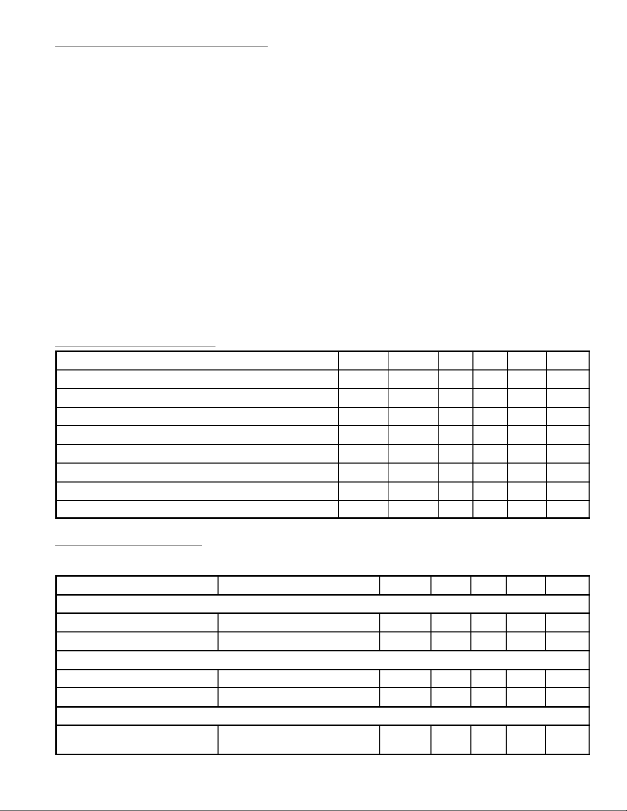
Standard Operating Range:
Parameter Symbol PIN # Min Typ Max Units
Analog Supply Voltage V
Analog Supply Current I
Injector Supply Voltage V
Total Dissipation, no external loads P
Force Asynchronous Low (“0”) V
Force Asynchronous V
Integrated Vertical, Low V
Integrated Vertical, High V
CC
CC
INJ
D
FAL
FAH
IVL
IVH
7 10.9 12.0 12.9 V
7 30 45 60 mA
10 1.3 1.6 1.9 V
– – 580 – mW
2 –0.5 0 +0.25 V
2 0.7 0.8 1.5 V
1 – – 1.9 V
1 2.8 – – V
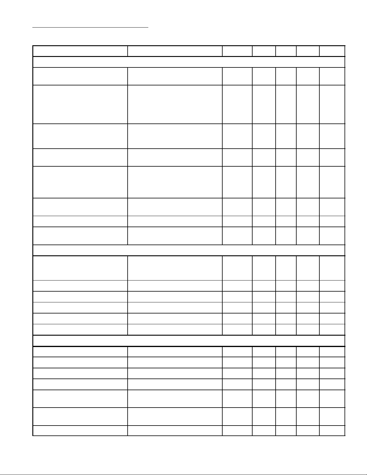
Electrical Characteristics: (TA = +25°C, VCC = 12VDC, V25 = 12VDC, Pin 2, 15, 22 to GND;, 1µF
from Pin 4 to GND., 10K ohms from Pin 28 to GND., F
4V, V
Power Supply Section
Supply Current Pin 10 Open 7 20 45 60 mA
1.9V to 2.8V, VFA 0.2V to 0.7V)
IV
Parameter Test Conditions PIN # Min Typ Max Units
= 1MHz, (AC Coupled), V
CLK
Sync
1.2V to
Injector Voltage 10 1.3 1.6 1.9 V
Sync Separator/Diff. Section
Video Inverter, High Voltage V27 = 4V, I26 = –500µA 26 4.2 5.1 5.8 V
Sync Processor, Low Voltage V27 = 4V, I26 = 0µA 28 – – .1 V
OSC/Count–Down/APC Section
APC Bias V27 = 4V, I26 = 0µA,
21 6.5 6.8 7.5 V
V21 = Open
Page 3
Electrical Characteristics (Cont’d): (TA = +25°C, VCC = 12VDC, V25 = 12VDC, Pin 2, 15, 22 to
GND;, 1µF from Pin 4 to GND., 10K ohms from Pin 28 to GND., F
1.2V to 4V, VIV 1.9V to 2.8V, VFA 0.2V to 0.7V)
V
Sync
Parameter Test Conditions PIN # Min Typ Max Units
OSC/Count–Down/APC Section (Cont’d)
= 1MHz, (AC Coupled),
CLK
APC Discharge V27 = 4V, I26 = 0µA,
21 6.5 6.8 7.5 V
V21 = Open
APC Discharge I26 = –500µA, V20 = 2V,
21 600 803 1100 µA
V21 = 2V,
V21 = VAPC Bias (above),
(Stop Clock When Pin 21
Goes Low)
APC Charge V27 = 4V, I26 = –500µA,
21 –600 –793 –1100 µA
V20 = 6V,
V21 = VAPC Bias (above)
Phase Detector I21 = APC Discharge–APC
21 –30 9.8 30 µA
Charge
Sync Width, Wide
Differentiation
V27 = 5V, V23 = 1MHz,
I20 = –300µA,
21 5 6 8 µs
V26 = Sq. Wave 0 to 5V with
T
= T
on
Sync Width, Narrow Same as above except
T
on
= 31.75µs
off
= 2µs, T
= 61.5µs
off
21 1.8 2.3 2.6 µs
Phase Detector Bias V27 = 4V 20 3.9 4.3 4.7 V
Oscillator Current 1 V24 = 3V, V23 = 6V
25 1.4 1.8 3.0 mA
V21 = 8.5V
OSC/Count–Down/APC Section
Oscillator Current Ratio V24 = 3V, V23 = 6V,
25 .45 .5 .55 Ratio
V21 = Open, Measured I25 &
Divide by Oscillator Current 1
Oscillator Bias 24 4.5 4.8 5.5 V
+Phase Input Current V24 = 0V 24 –230 312 –570 µA
–Phase Input Current V23 = 0V 23 –230 331 –570 µA
Flyback Charge Current V17 = 0V, V19 = 6V 19 –400 –501 –766 µA
Flyback Discharge Current I17 = 700µA, V19 = 6V 19 2 2.4 3.5 mA
Blanking/Gating Section
Flyback Input, Low Current 1 V18 = 0V 18 –3 –1 3 µA
Flyback Input, High Current 1 V18 = 2V 18 0.8 1.6 3.8 mA
Flyback Input, Low Current 2 V17 = 0V 17 –3 –.09 3 µA
Flyback Input, High Current 2 V17 = 2V 17 0.8 1.5 1.9 mA
Blanking Voltage V18 = 2V, V23 = 1MHz, Stop
16 5.8 6 6.4 V
Clock when 3V < V16< 5V
Burst Voltage V18 = 2V, V23 = 1MHz, Stop
16 11.2 11.95 – V
Clock when V16 > 9V
Burst Saturation Voltage V18 = 0V I16 = 5µA 16 – .45 0.6 V
Page 4

Electrical Characteristics (Cont’d): (TA = +25°C, VCC = 12VDC, V25 = 12VDC, Pin 2, 15, 22 to
GND;, 1µF from Pin 4 to GND., 10K ohms from Pin 28 to GND., F
1.2V to 4V, VIV 1.9V to 2.8V, VFA 0.2V to 0.7V)
V
Sync
Parameter Test Conditions PIN # Min Typ Max Units
Blanking/Gating Section (Cont’d)
Horizontal Blanking Starts (See Notes: 1, 2, 4) 16 – .07 0.6 µs
Horizontal Blanking Width (See Notes: 2, 4, 5) 16 11.75 12.3 12.75 µs
Burst Gate Starts (See Notes: 1, 2, 4) 16 0.15 .44 0.45 µs
Burst Gate Trailing Edge (See Notes: 1, 2, 4) 16 8.6 – 9.8 µs
AGC Gate Starts (See Notes: 1, 2, 4) 9 – .37 0.9 µs
AGC Gate Width 1 (See Notes: 2, 4, 5) 9 4.25 5.3 6.25 µs
AGC Gate Width 2 (See Notes: 3, 4, 5) 9 4.25 5.2 6.25 µs
Horizontal Drive Section
= 1MHz, (AC Coupled),
CLK
Horizontal Out, Low Voltage
Start
Low Voltage Horizontal Period VCC = 3V, V23 = 1MHz
VCC = 3V, 50pF (Pin 3 to GND),
3.9 K–ohm (Pin 3 to 3V)
3 2.8 – – V
P–P
3 55 64 75 µs
50pF (Pin 3 to GND),
3.9K–ohm (Pin 3 to 3V)
(Trigger Level 1.5V)
Low Voltage Horizontal Pulse
Width Symmetry
VCC = 3V, V23 = 1MHz,
50pF (Pin 3 to GND),
3 .3 .48 .7 Ratio
3.9K–ohm (Pin 3 to 3V)
(Trigger Level 1.5V)
Find Pulse Width Divide
by Period
Pin 4 Quiescent Voltage V6 = V8 = 6V, I5 = 20mA,
8.4 8.7 9.1 V
Pin 4 Open
Horizontal Drive Saturation
V6 = V8 = 6V 5 – 174 225 mV
Voltage
Horizontal Drive Symmetry V6 = V8 = 6V,
5 26 29.5 33 µs
200 ohm (Pin 5 to GND),
600 ohm (Pin 5 to V
V4 = 15, 734Hz, 2V
CC
p–p
),
Horizontal Drive Ratio 3 – 64 – µs
Horizontal Pulse Width 3 31 – 33 µs
Vertical Drive Section
Ramp Leakage V12 = 0V, V11 = 1V, V13 = 4V 11 – .04 –3 µA
Mirror Ramp Current I12 = 150µA, V11 = 4V,
11 – .04 –3 µA
V13 = 5V
Ramp Charging Current,
VD High
V12 = 0V, V11 = 0V, V13 = 5V,
Stop Clock when Pin 11 Goes
11 –5.5 –10 –15.5 mA
High
Page 5

Electrical Characteristics (Cont’d): (TA = +25°C, VCC = 12VDC, V25 = 12VDC, Pin 2, 15, 22 to
GND;, 1µF from Pin 4 to GND., 10K ohms from Pin 28 to GND., F
1.2V to 4V, VIV 1.9V to 2.8V, VFA 0.2V to 0.7V)
V
Sync
Parameter Test Conditions PIN # Min Typ Max Units
Vertical Drive Section (Cont’d)
= 1MHz, (AC Coupled),
CLK
Amplifier Input Voltage
Range, VD Low
100ohm (Pin 14 to GND)
V13 = 1.7V,
Set V11 for V14 = 2V
Record V11, 13; Then V13 = 4V
Record V11, 13;
Find Difference Stop Clock
When Pin Goes Low
Vertical, On–State Voltage V12 = 0V, V11 = 3V, V13 = 5V,
I14 = –45 mA
Vertical, Off–State Current V12 = 0V, V11 = 4V, V13 = 3V,
V14 = 5V
Open Loop, Small Signal
Voltage Gain
100 ohm (Pin 14 to GND)
V13 = 2V
Set V11 thru 1K ohm for
V14 = 2V
Apply 1kHz, 1V
RMS
to Pin 11
Thru 99 K ohm and 1µF
Avol = 20 LOG|V14 (AC)/V11
(AC))
Mode Change
Non–Standard IV Field
Sync = 9, Within IV Window
(See Note 6)
Count STD/NON–STD
Mode Change
Sync = Less than 9 11,16 5 – 7 –
Non–Standard Vertical
Sync Field
Count STD/NON–STD
11,13 – – 50 mV
14 1.4 – – V
14 – – 2 µA
11,14 24 33 39 dB
11,16 5 – 7 –
Mode Change
Field Confidence Count,
NON–STD/STD
Number of New Timing
IV/Sync Periods to Return to
STD Mode
Standard Mode Divide Ratio IV = 16800
Clock Ratio Sync = 9 )
Serrations within 384 Clock
Window (After 8 Fields, i.e: On
9th Field)
Standard Mode Vertical
Pulse Width
(See Note 7)
Number of Clock Cycles
Output is On
Non–Standard Mode IV Ratio Range Can Be and
Cause Proper Syncronization,
Except for IV Ratio Range of
(16748–16832), Sync = Don’t
Care (After 7 Fields, i.e.: on
8th Field)
Non–Standard Vertical
Pulse Width
Number of Clock Cycles
Output is On
11,16 7 – 14 –
– – – 16800
11 383 384 387 –
– 16160 – 17405
11 362 364 367 –
Page 6

Electrical Characteristics (Cont’d): (TA = +25°C, VCC = 12VDC, V25 = 12VDC, Pin 2, 15, 22 to
GND;, 1µF from Pin 4 to GND., 10K ohms from Pin 28 to GND., F
1.2V to 4V, VIV 1.9V to 2.8V, VFA 0.2V to 0.7V)
V
Sync
Parameter Test Conditions PIN # Min Typ Max Units
Vertical Drive Section (Cont’d)
= 1MHz, (AC Coupled),
CLK
Non–Standard Vertical
Pulse Width
Non–Standard Mode Asynchronous Divide Ratio
Blanking Pulse Width – 16 1200 1216 1220 –
Noise Mode Change IV Outside the Range of
Force Non–Standard Mode IV = 16800 Sync = 9 Serra-
Sync 9 Serrations Within 384
Clock Window, Number of
Clock Cycles Output is On
No IV or Sync Applied (After 7
Fields, i.e., on 8th Field)
(16784–16832) Sync = 9
Serrations in 384 Clock Window Pulse Applied 2432 to
11520 After an IV, Pulse is 8
to 32 Clocks Wide. Resync
results in next field and is
maintained for Mode Change
Confidence Count
tions Within 384 Clock Window. VFA Open Circuit Vertical Pulse Width M Measured
in Next Field.
11 362 364 367 –
11, 16 – – 21888 –
11,16 – – 16800 –
11 362 364 367 µs
Note 1 All timing measurements are with reference to the leading edge of the fly–back pulse input
to Pin 18. Fly–back pulse width is 12.00 µs and it is from 0 to 5V . Fly–back pulse train should
start about 500 µs after the start of vertical drive pulse.
Note 2 Start of fly–back pulse is 90 degrees leading with clock.
Note 3 Start of fly–back pulse is 90 degrees lagging with clock.
Note 4 Threshold for measuring AGC gate and horizontal blanking is 3V and burst gate is at 9V.
Note 5. Timing measurements referenced to trailing edge of negative sync pulse input to Pin 26. Th e
negative sync pulse width is is 4.5µs and is from 0 to 500µA, with negative leading edge
delayed 0.5µs from the positive leading edge of the fly–back pulse. The input to Pin 27 is
DC
.
+4V
Note 6 IV Ratio same as in Non–Standard Mode Ratio Range Test.
Note 7 IV Ratio same as in Standard Mode Ratio Test.
Note 8 Burst Gate Start is with reference to trailing edge of sync pulse at Pin 26. Sync Pulse is a
500µA Sink Current at Pin 26
.
Page 7

Pin Connection Diagram
Integrated Vert Input
Mode Select
Horiz Output
Horiz Sawtooth Input
V
CC
Beam Current
Feedback Ref
Vert Ramp Shape
Vert Height Adjust
Vert Feedback
1
2
3
4
5Horiz Drive Output
6B+ Adjust Ref
7
8
9AGC Gate Output 20
10Shunt Reg
11
12 17
13
14Vert Output 15
28
27
26
25
24 OSC Tank Lag Input
23
22
21
19
18
16
Sync Output
Composite Video Input
Sync Sep Filter
OSC Tank
OSC tank Lead Input
GND
APC Filter
Flyback Sawtooth Ramp
Flyback Sawtooth Filter
Flyback Input 1
Flyback Input 2
Sandcastle Output
Vert GND
14 1
15 28
1.469 (37.32)
Max
.100 (2.54)
1.300 (33.02)
.250
(6.35)
.122
(3.1)
Min
.540
(13.7)
.600
(15.24)
 Loading...