

Page 1

NTE888M
Integrated Circuit
Low Power Programmable Operational Amplifier
Description:
The NTE888M is an operational amplifier in an 8–Lead DIP type package featuring low power consumption and high input impedance. In addition, the quiescent currents within this device may be
programmed by the choice of an external resistor value or current source applied to the I
This allows the NTE888M’s characteristics to be optimized for input current and power consumption
despite wide variations in operating power supply voltages.
Features:
D ±1.2V to ±18V Operation
D Wide Programming Range
D Offset Null Capability
D No Frequency Compensation Required
D Low Input Bias Currents
D Short–Circuit Protection
SET
input.
Maximum Ratings
Power Supply Voltages, V
Differential Input Voltage, V
Common–Mode Input Voltage, V
VCC and |VEE| < 15V VCC, V
V
and |VEE| ≥ 15V ±15V. . . . . . . . . . . . . . . . . . . . . . . . . . . . . . . . . . . . . . . . . . . . . . . . . . . . . . . .
CC
Offset Null to V
Programming Current, I
Programming Voltage, V
Voltage from I
Output Short–Circuit Duration (Note 1), t
Operating Temperature Range, T
Storage Temperature Range, T
Junction Temperature, T
: (TA = +25°C unless otherwise noted)
, V
CC
EE
±30V. . . . . . . . . . . . . . . . . . . . . . . . . . . . . . . . . . . . . . . . . . . . . . . . . . . . . . .
ID
ICM
. . . . . . . . . . . . . . . . . . . . . . . . . . . . . . . . . . . . . . . . . . . . . . . . . . . . .
Voltage, V
EE
SET
set
SET
terminal to GND (VCC –2V) to V
J
– V
off
EE
500µA. . . . . . . . . . . . . . . . . . . . . . . . . . . . . . . . . . . . . . . . . . . . . . . . . . . . . . . .
. . . . . . . . . . . . . . . . . . . . . . . . . . . . . . . . . .
s
0° to +70°C. . . . . . . . . . . . . . . . . . . . . . . . . . . . . . . . . . . . . . . . . . . .
A
–55° to +125°C. . . . . . . . . . . . . . . . . . . . . . . . . . . . . . . . . . . . . . . . . .
stg
+150°C. . . . . . . . . . . . . . . . . . . . . . . . . . . . . . . . . . . . . . . . . . . . . . . . . . . . . . . .
±18V. . . . . . . . . . . . . . . . . . . . . . . . . . . . . . . . . . . . . . . . . . . . . . . . . . .
EE
±0.5V. . . . . . . . . . . . . . . . . . . . . . . . . . . . . . . . . . . . . . . . . . . . . . .
CC
Indefinite. . . . . . . . . . . . . . . . . . . . . . . . . . . . . . . . . . . . . . . .
Note 1. May be t o GND or either Supply Voltage. Rating applies up to a case temperature of +125°C
or ambient temperature of +70°C and I
SET
≤ 30µA.
Page 2
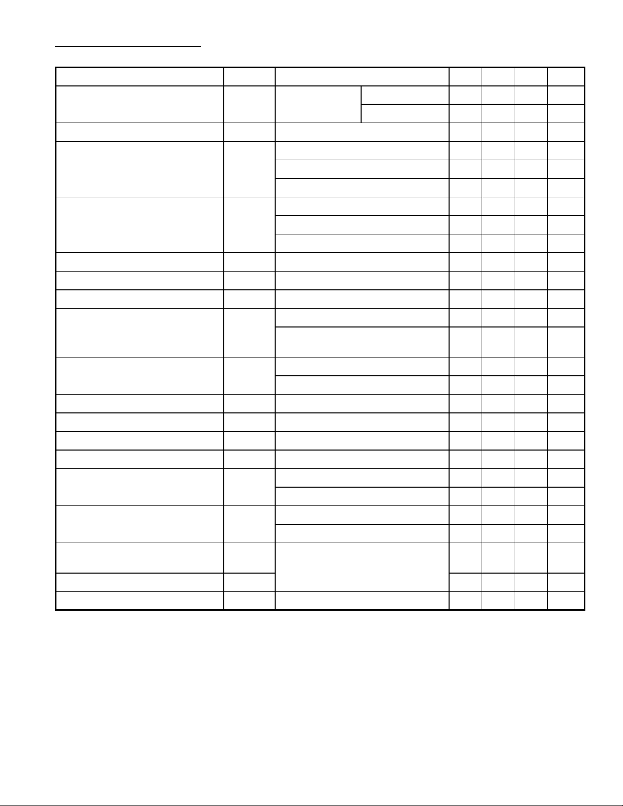
Electrical Characteristics:(VCC = +15V, VEE = –15V, I
wise specified)
Parameter Symbol Test Conditions Min Typ Max Unit
= 15µA, TA = +25°C unless other–
SET
Input Offset Voltage V
Offset Voltage Adjustment Range V
Input Offset Current I
Input Bias Current I
Input Resistance r
Input Capacitance c
Input Voltage Range V
Large Signal Voltage Gain A
Output Voltage Swing V
IO
IOR
IO
IB
i
i
ID
VOL
O
RS ≤ 10kΩ – 2 6 mV
0° ≤ TA ≤ +70°C – – 7.5 mV
– 18 – mV
– 2 25 nA
TA = +70°C – – 25 nA
TA = 0°C – – 40 nA
– 15 50 nA
TA = +70°C – – 50 nA
TA = 0°C – – 100 nA
– 5 – MΩ
– 2 – pF
0° ≤ TA ≤ +70°C ±10 – – V
RL ≥ 5kΩ, VO = ±10V 50k 400k – V/V
RL ≥ 75kΩ, VO = ±10V,
0° ≤ T
≤ +70°C
A
50k – – V/V
RL ≥ 5kΩ ±10 ±13 – V
RL ≥ 75kΩ, 0° ≤ TA ≤ +70°C ±10 – – V
Output Resistance r
Output Short–Circuit Current I
o
os
– 1 – kΩ
– 12 – mA
Common–Mode Rejection Ratio CMRR RL ≤ 10kΩ, 0° ≤ TA ≤ +70°C 70 90 – dB
Supply Voltage Rejection Ratio PSRR RL ≤ 10kΩ, 0° ≤ TA ≤ +70°C – 25 200 µV/V
Supply Current ICC, I
EE
– 160 190 µA
0° ≤ TA ≤ +70°C – – 200 µA
Power Dissipation P
D
– 5.7 mW
0° ≤ TA ≤ +70°C – – 6.0 mW
Transient Response (Unity Gain)
Rise Time
t
TLH
Vin = 20mV, RL ≥ 5kΩ, CL = 100pF – 0.35 – µs
Overshoot OS – 10 – %
Slew Rate
S
RL ≥ 5kΩ – 0.8 – V/µs
R
Page 3

Pin Connection Diagram
Offset Null 1
Inverting Input
Non–Inverting Input
VCC (–)
85
1
2
3
4
8
I
SET
7
6
5
(+)
V
CC
Output
Offset Null 2
.260 (6.6)
.100 (2.54)
14
.390 (9.9)
Max
.155
(3.93)
.300 (7.62)
.300
(7.62)
.145 (3.68)
 Loading...