

Datasheet NE56632-31D, NE56632-43D, NE56632-45D, NE56632-46D, NE56632-30D Datasheet (Philips)
...Page 1

INTEGRATED CIRCUITS
NE56632-XX
Active-LOW system reset
with adjustable delay time
Product data 2002 Mar 25
Page 2
Philips Semiconductors Product data
NE56632-XXActive-LOW system reset with adjustable delay time
DESCRIPTION
The NE56632-XX is a family of Active-LOW, power-on reset that
offers precision threshold voltage detection within ±1.5% and super
low operating supply current of typically 3.0 µA. It includes a reset
delay that is user adjustable with an external capacitor.
Several detection threshold voltages are available at 1.9V , 2.0 V ,
2.7 V, 2.8 V, 2.9 V, 3.0 V, 3.1 V, 4.2 V, 4.3 V, 4.4 V, 4.5 V, and 4.6 V.
Other thresholds are offered upon request at 100 mV steps from
1.9 V to 4.6 V.
With its ultra low supply current and high precision voltage threshold
detection capability, the NE56632-XX is well suited for various
battery powered applications such as reset circuits for logic and
microprocessors, voltage check, and level detecting. It is available in
the SOT23-5 package.
FEA TURES
•High precision threshold detection voltage: V
±1.5%
S
•Super low operating supply current: 3 µA typ.
•Built-in hysteresis voltage: 50 mV typ.
•Detection threshold voltage: 1.9 V, 2.0 V , 2.7 V, 2.8 V, 2.9 V,
3.0 V, 3.1 V, 4.2 V, 4.3 V, 4.4 V, 4.5 V, and 4.6 V.
•Reset Output: Active-LOW, open collector
•Other detection threshold voltages available upon request at
100 mV steps from 1.9 V to 4.6 V.
•Large low reset output current: 30 mA typ.
•Power-on reset delay time adjustable with external capacitor:
200 µs to 200 ms
•Reset assertion with V
SIMPLIFIED SYSTEM DIAGRAM
TO V
CC
down to 0.65 V
CC
R
PU
NE56632-XX
TO RESET
TERMINAL
OF CPU
45
APPLICATIONS
•Reset for microprocessor and logic circuits
•Voltage level detection circuit
•Battery voltage check circuit
•Detection circuit for battery back-up
123
C
D
SL01605
Figure 1. Simplified system diagram.
2002 Mar 25 853–2329 27919
2
Page 3
Philips Semiconductors Product data
TYPE NUMBER
NE56632-XXActive-LOW system reset with adjustable delay time
ORDERING INFORMATION
PACKAGE
NAME DESCRIPTION
NE56632-XXD SOT23-5 / SOT25 (SO5) plastic small outline package; 5 leads (see dimensional drawing) –20 to +75 °C
NOTE:
The device has 12 voltage output options, indicated by the XX on
the ‘Type number’.
XX
VOLTAGE (Typical)
19 1.9 V
20 2.0 V
27 2.7 V
28 2.8 V
29 2.9 V
30 3.0 V
31 3.1 V
42 4.2 V
43 4.3 V
44 4.4 V
45 4.5 V
46 4.6 V
Part number marking
The package is marked with a four letter code. The first three letters
designate the product. The fourth letter, represented by ‘x’, is a date
tracking code.
Part Number
NE56632-19D AKZx
NE56632-20D ALAx
NE56632-27D ALBx
NE56632-28D ALCx
NE56632-29D ALDx
NE56632-30D ALEx
NE56632-31D ALFx
NE56632-42D ALGx
NE56632-43D ALHx
NE56632-44D ALJx
NE56632-45D ALKx
NE56632-46D ALLx
Marking
TEMPERATURE
RANGE
PIN CONFIGURATION
PIN DESCRIPTION
PIN SYMBOL DESCRIPTION
1 TC Delay time control; set with external
capacitor.
2 SUB Substrate. Connect to ground (GND).
SUB
1
TC
2
NE56632-XX
5V
CC
3 GND Ground. Negative supply.
34
GND
SL01604
V
OUT
4 V
5 V
OUT
CC
Reset output voltage. Active-LOW.
Positive supply voltage; detection threshold
voltage input.
Figure 2. Pin configuration.
MAXIMUM RATINGS
SYMBOL PARAMETER MIN. MAX. UNIT
V
CC
T
amb
T
stg
P Power dissipation – 150 mW
Supply voltage –0.3 +10 V
Ambient operating temperature –20 +75 °C
Storage temperature –40 +125 °C
2002 Mar 25
3
Page 4
Philips Semiconductors Product data
V
(Fig
)
Test Circuit 1 (Figure 27)
NE56632-XXActive-LOW system reset with adjustable delay time
ELECTRICAL CHARACTERISTICS
T
= 25 °C, unless otherwise specified.
amb
SYMBOL
V
S
V
hys
VS/∆T Detection threshold voltage
V
OL
I
LO
I
CCL
I
CCH
t
PLH
t
PHL
V
OPL
I
OL1
I
OL2
NOTES:
1. t
:VCC = (V
PLH
:VCC = (V
2. t
PHL
3. See Table 1.
PARAMETER CONDITIONS -XX MIN. TYP. MAX. UNIT
Detection threshold VCC = HIGH-to-LOW; RL = 4.7 kΩ; S1=ON;
≤ 0.4 V;
OL
Test Circuit 1
ure 27
46
45
44
43
42
31
30
29
28
27
20
19
Hysteresis voltage RL = 4.7 kΩ; VCC = LOW-to-HIGH-to-LOW; S1 = ON; Test
4.531 4.600 4.669 V
4.432 4.500 4.568 V
4.334 4.400 4.466 V
4.235 4.300 4.365 V
4.137 4.200 4.263 V
3.053 3.100 3.147 V
2.955 3.000 3.045 V
2.856 2.900 2.944 V
2.758 2.800 2.842 V
2.659 2.700 2.741 V
1.970 2.000 2.030 V
1.871 1.900 1.929 V
25 50 100 mV
Circuit 1 (Figure 27)
temperature coefficient
LOW-level output voltage V
Output leakage current V
Supply current (ON time) V
Supply current (OFF time) V
CC1
CC1
CC1
RL = 4.7 kΩ; T
= V
CC1
= V
= 10 V; S2 = ON; Test Circuit 1 (Figure 27) – – ±0.1 µA
CC2
= V
S(min)
= V
S(typ)
= –20 °C to +75 °C; S1 = ON;
amb
Test Circuit 1 (Figure 27)
– 0.05 V; RL = 4.7 kΩ; S1 = ON;
S(min)
Test Circuit 1 (Figure 27)
– ±0.01 – %/°C
– 0.2 0.4 V
– 0.05 V; RL = ∞; Test Circuit 1 (Figure 27) – 5.0 9.0 µA
/0.85; RL = ∞; Test Circuit 1 (Figure 27) – 3.0 5.0 µA
LOW-to-HIGH delay time CL = 100 pF; RL = 4.7 kΩ; CD = 10 nF (Note 1) – (Note 3) – ms
HIGH-to-LOW delay time CL = 100 pF; RL = 4.7 kΩ; CD = 10 nF (Note 2) – (Note 3) – µs
Minimum operating
threshold voltage
Output current (ON Time 1) VO = 0.4 V; RL = 0; V
Output current (ON Time 2) VO = 0.4 V; RL = 0; V
– 0.4 V) to (V
S(typ)
+ 0.4 V) to (V
S(typ)
S(typ)
S(typ)
+ 0.4 V); t
– 0.4 V); t
RL = 4.7 kΩ; VOL ≤ 0.4 V; S1 = ON;
Test Circuit 1 (Figure 27)
= V
CC1
CC1
= V
S(min)
S(min)
V
= 0.4 V; S2 = ON; Test Circuit 1 (Figure 27)
CC2
T
= –20 °C to +75 °C; S2 = ON;
amb
Test Circuit 1 (Figure 27)
is release delay time (Test Circuit 2, Figure 28).
PLH
is assertion delay time (Test Circuit 2, Figure 28).
PHL
– 0.05 V;
– 0.05 V;
– 0.65 0.80 V
5 – – mA
3 – – mA
Table 1. NE56632-XX series typical delay time
–XX t
PLH
46 195 ms 140 µs
45 190 ms 140 µs
44 185 ms 140 µs
43 180 ms 140 µs
42 175 ms 140 µs
31 120 ms 120 µs
30 115 ms 120 µs
29 110 ms 120 µs
28 105 ms 100 µs
27 100 ms 100 µs
20 65 ms 100 µs
19 60 ms 100 µs
2002 Mar 25
t
PHL
4
Page 5

Philips Semiconductors Product data
NE56632-XXActive-LOW system reset with adjustable delay time
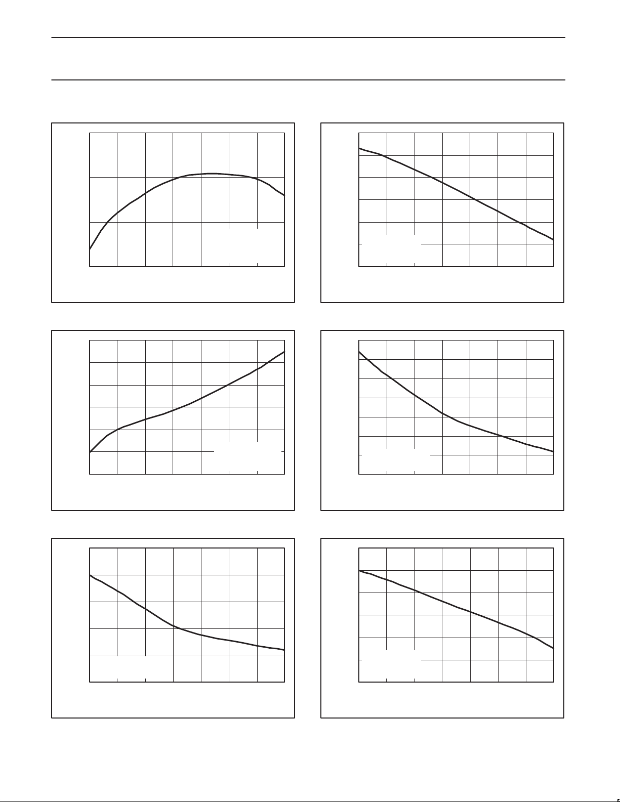
TYPICAL PERFORMANCE CURVES, NE56632-20
2.0050
2.0025
2.0000
1.9975
1.9950
1.9925
, DETECTION THRESHOLD (V)
S
V
1.9900
1.9875
1.9850
–40 –20
0 20 40 60 80 100
AMBIENT TEMPERATURE, T
Test Circuit 1
VCC = HIGH-to-LOW
= 4.7 kΩ
R
L
VOL ≤ 0.4 V
S1 = ON
(°C)
amb
SL01620
Figure 3. Detection threshold versus temperature.
0.225
0.220
0.215
0.210
0.205
0.200
, LOW-LEVEL OUTPUT VOLTAGE (V)
V
OL
0.195
0.190
0.185
–40 –20
0 20 40 60 80 100
AMBIENT TEMPERATURE, T
Test Circuit 1
V
= V
CC1
S(min)
RL = 4.7 kΩ
S1 = ON
(°C)
amb
– 0.05 V
SL01622
Figure 5. LOW-level output voltage versus temperature.
100
90
80
70
60
50
, HYSTERESIS VOLTAGE (mV)
Test Circuit 1
hys
VCC = LOW-to-HIGH-to-LOW
V
40
RL = 4.7 kΩ
S1 = ON
30
–40 –20
0 20 40 60 80 100
AMBIENT TEMPERATURE, T
amb
(°C)
SL01621
Figure 4. Hysteresis voltage versus temperature.
9
8
7
6
5
, SUPPLY CURRENT (ON time), ( A)µ
4
Test Circuit 1
CCL
I
V
= V
CC1
= ∞
R
L
3
–40 –20
– 0.05 V
S(min)
0 20 40 60 80 100
AMBIENT TEMPERATURE, T
amb
(°C)
SL01623
Figure 6. Supply current (ON time) versus temperature.
4.5
4.0
3.5
3.0
2.5
, SUPPLY CURRENT (OFF time), ( A)µ
I
CCH
Test Circuit 1
RL = ∞
V
CC1
2.0
–40 –20
= V
/0.85
S(typ)
0 20 40 60 80 100
AMBIENT TEMPERATURE, T
amb
(°C)
Figure 7. Supply current (OFF time) versus temperature.
2002 Mar 25
SL01624
0.9
0.8
0.7
0.6
0.5
Test Circuit 1
0.4
RL = 4.7 kΩ
VOL ≤ 0.4 V
S1 = ON
, MIN. OPERATING THRESHOLD VOLTAGE (V)
0.3
OPL
–40 –20
V
0 20 40 60 80 100
AMBIENT TEMPERATURE, T
amb
(°C)
Figure 8. Min. operating threshold voltage versus temperature.
5
SL01625
Page 6

Philips Semiconductors Product data
NE56632-XXActive-LOW system reset with adjustable delay time
TYPICAL PERFORMANCE CURVES, NE56632-20
37
35
33
31
29
Test Circuit 1
V
= V
CC1
V
CC2
27
, OUTPUT CURRENT (ON Time 1), (mA)
VO = 0.4 V
RL = 0 Ω
OL1
I
S2 = ON
25
–40 –20
Figure 9. Output current (ON time 1) versus temperature.
120
Test Circuit 2
CL = 100 pF
115
RL = 4.7 kΩ
CD = 10 nF
110
105
100
95
90
PHL, HIGH-to-LOW DELAY TIME ( s)µ
t
85
80
–40 –20
Figure 11. HIGH-to-LOW delay time versus temperature.
– 0.05 V
S(min)
= 0.4 V
0 20 40 60 80 100
AMBIENT TEMPERATURE, T
0 20 40 60 80 100
AMBIENT TEMPERATURE, T
VCC = (V
t
PHL
+ 0.4 V) to (V
S(typ)
= Assertion Delay Time
amb
amb
(°C)
(°C)
S(typ)
SL01626
– 0.4 V)
SL01628
(continued)
100
Test Circuit 2
CL = 100 pF
RL = 4.7 kΩ
90
CD = 10 nF
80
70
60
, LOW-to-HIGH DELAY TIME (ms)
PLH
50
t
40
–40 –20
AMBIENT TEMPERATURE, T
VCC = (V
t
PLH
0 20 40 60 80 100
– 0.4 V) to (V
S(typ)
= Release Delay Time
(°C)
amb
S(typ)
+ 0.4 V)
SL01627
Figure 10. LOW-to-HIGH delay time versus temperature.
2002 Mar 25
6
Page 7
Philips Semiconductors Product data
NE56632-XXActive-LOW system reset with adjustable delay time
TYPICAL PERFORMANCE CURVES, NE56632-31
3.11
3.10
3.09
Test Circuit 1
, DETECTION THRESHOLD (V)
S
V
3.08
–40 –20
0 20 40 60 80 100
AMBIENT TEMPERATURE, T
VCC = HIGH-to-LOW
RL = 4.7 kΩ
VOL ≤ 0.4 V
S1 = ON
(°C)
amb
SL01629
Figure 12. Detection threshold versus temperature.
0.23
0.22
0.21
0.20
0.19
0.18
, LOW-LEVEL OUTPUT VOLTAGE (V)
OL
V
0.17
–40 –20
0 20 40 60 80 100
AMBIENT TEMPERATURE, T
Test Circuit 1
V
= V
CC1
S(min)
RL = 4.7 kΩ
S1 = ON
(°C)
amb
– 0.05 V
SL01631
Figure 14. LOW–level output voltage versus temperature.
90
80
70
60
50
Test Circuit 1
, HYSTERESIS VOLTAGE (mV)
40
VCC = LOW-to-HIGH
hys
RL = 4.7 kΩ
V
S1 = ON
30
–40 –20
0 20 40 60 80 100
AMBIENT TEMPERATURE, T
amb
(°C)
SL01630
Figure 13. Hysteresis voltage versus temperature.
9
8
7
6
5
4
, SUPPLY CURRENT (ON time), ( A)µ
Test Circuit 1
3
CCL
I
V
= V
CC1
= ∞
R
L
2
–40 –20
– 0.05 V
S(min)
0 20 40 60 80 100
AMBIENT TEMPERATURE, T
amb
(°C)
SL01632
Figure 15. Supply current (ON time) versus temperature.
4.5
4.0
3.5
3.0
2.5
, SUPPLY CURRENT (OFF time), ( A)µ
Test Circuit 1
RL = ∞
CCH
I
V
= V
CC1
2.0
–40 –20
/0.85
S(typ)
0 20 40 60 80 100
AMBIENT TEMPERATURE, T
amb
(°C)
Figure 16. Supply current (OFF time) versus temperature.
2002 Mar 25
SL01633
0.9
0.8
0.7
0.6
0.5
Test Circuit 1
0.4
RL = 4.7 kΩ
VOL ≤ 0.4 V
, MIN. OPERATING THRESHOLD VOLTAGE (V)
S1 = ON
0.3
OPL
V
–40 –20
0 20 40 60 80 100
AMBIENT TEMPERATURE, T
amb
(°C)
SL01634
Figure 17. Min. operating threshold voltage versus
temperature.
7
Page 8

Philips Semiconductors Product data
NE56632-XXActive-LOW system reset with adjustable delay time
TYPICAL PERFORMANCE CURVES, NE56632-31
36
34
32
30
28
26
Test Circuit 1
V
= V
24
CC1
V
, OUTPUT CURRENT (ON Time 1), (mA)
OL1
I
CC2
VO = 0.4 V
22
RL = 0 Ω
S2 = ON
20
–40 –20
Figure 18. Output current (ON time 1) versus temperature.
180
Test Circuit 2
CL = 100 pF
160
RL = 4.7 kΩ
CD = 10 nF
140
120
100
80
, LOW-to-HIGH DELAY TIME (ms)
PLH
t
60
40
–40 –20
Figure 20. LOW-to-HIGH delay time versus temperature.
– 0.05 V
S(min)
= 0.4 V
0 20 40 60 80 100
AMBIENT TEMPERATURE, T
0 20 40 60 80 100
AMBIENT TEMPERATURE, T
VCC = (V
t
PLH
– 0.4 V) to (V
S(typ)
= Release Delay Time
amb
amb
(°C)
(°C)
S(typ)
SL01635
+ 0.4 V)
SL01637
(continued)
37
35
33
31
Test Circuit 1
V
= V
29
, OUTPUT CURRENT (ON Time 2), (mA)
OL2
I
27
–40 –20
CC1
V
CC2
VO = 0.4 V
RL = 0 Ω
S2 = ON
– 0.05 V
S(min)
= 0.4 V
0 20 40 60 80 100
AMBIENT TEMPERATURE, T
amb
(°C)
SL01636
Figure 19. Output current (ON time 2) versus temperature.
160
Test Circuit 2
CL = 100 pF
150
RL = 4.7 kΩ
CD = 10 nF
140
130
120
110
100
PHL, HIGH-to-LOW DELAY TIME ( s)µ
t
90
80
–40 –20
AMBIENT TEMPERATURE, T
VCC = (V
t
PHL
0 20 40 60 80 100
+ 0.4 V) to (V
S(typ)
= Assertion Delay Time
(°C)
amb
S(typ)
– 0.4 V)
SL01638
Figure 21. HIGH-to-LOW delay time versus temperature.
2002 Mar 25
8
Page 9
Philips Semiconductors Product data
NE56632-XXActive-LOW system reset with adjustable delay time
TECHNICAL DISCUSSION
The NE56632-XX is a bipolar IC designed to provide power source
monitoring and a system reset function in the event the power sags
below an acceptable level for the system to operate reliably. The
reset threshold incorporates a typical hysteresis of 50 mV to prevent
erratic reasserts from being generated. An internal delay time circuit
provides a adjustable power-on reset delay of typically 200 µs to
200 ms using an external capacitor.
The output of the NE56632-XX utilizes an open collector topology,
which requires an external pull-up resistor to V
be regarded as a disadvantage, it is advantageous in many
sensitive applications. Because the open collector output cannot
source reset current when both are operated from a common supply,
the NE56632-XX offers a safe interconnect to a wide variety of
microprocessors.
The NE56632-XX operates at low supply currents, typically 3 µA,
while offering precision threshold detection (±1.5%).
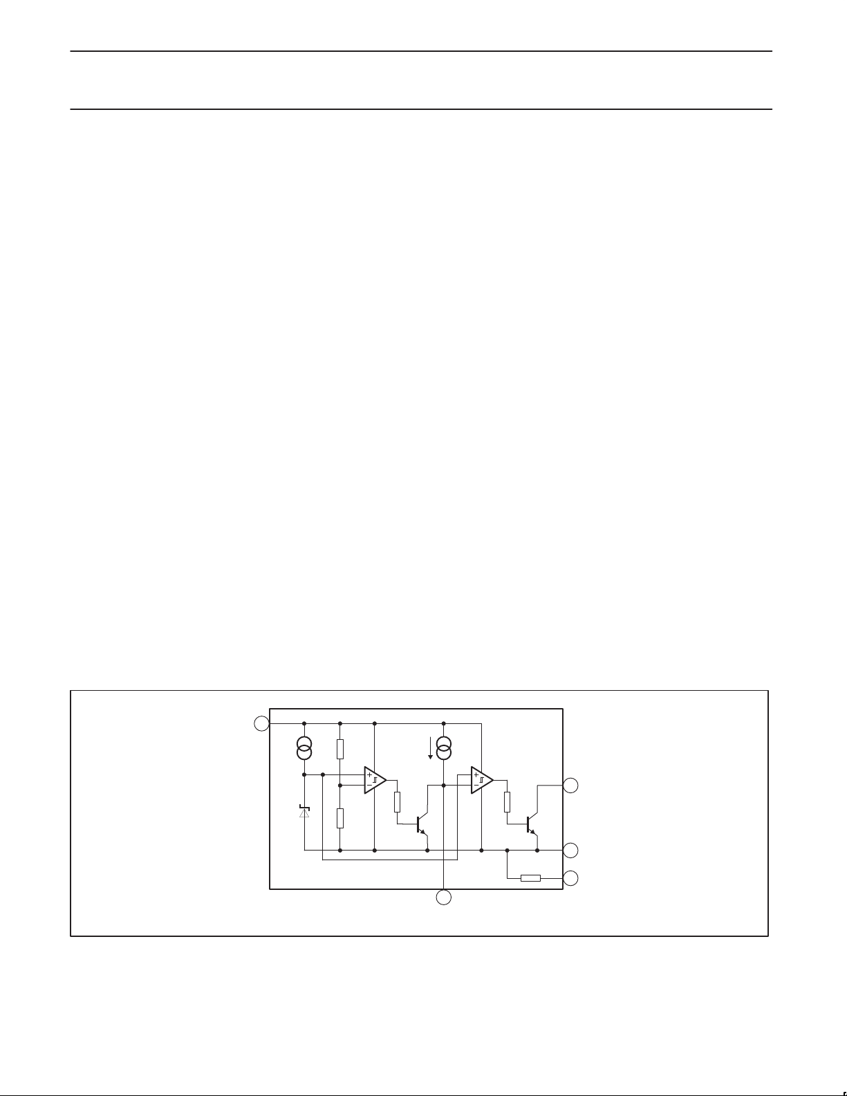
Figure 22 is a functional block diagram of the NE56632-XX. The
internal reference source voltage, V
, is typically 0.65 V over the
REF
temperature range. The reference voltage is connected to the
non-inverting inputs of the threshold Comparator 1 and
Comparator 2, while the inverting input of Comparator 1 monitors
the supply voltage through a voltage divider (R1 and R2). The output
of the comparator drives the series base resistor, R3 of a common
emitter amplifier , Q1. The collector of Q1 is connected to the
inverting terminal of Comparator 2. The output of Comparator 2 is
connected to the series base resistor, R4 of the output common
emitter transistor, Q2. The open collector output of Q2 provides the
reset output.
The Delay Time Control is outputted at the junction of the collector
of Q1 and the inverting input of Comparator 2. The reset release
time delay, t
show t
PLH
is set with an external capacitor. Figures 25 and 26
PLH
as a function of the external delay capacitor, CD.
When the supply voltage sags to the threshold detection voltage, the
resistor divider network supplies a voltage to the inverting terminal of
. Though this may
CC
the threshold comparator which is less than V
, causing the output
REF
of the comparator to go to a HIGH state. This causes the common
emitter amplifier , Q1 to turn ON pulling down the non-inverting
terminal of Comparator 2 which causes its output to go to a HIGH
state. This HIGH output level turns on the output common emitter
transistor, Q2. The collector output of Q2 is pulled LOW through the
external pull-up resistor, thereby asserting the Active-LOW reset.
Threshold hysteresis is established by turning on the bipolar common
emitter transistor, Q1 when the input threshold Comparator 1 goes
to a HIGH state. This occurs when V
sags to or below the
CC
threshold level. With the output of Q1 connected to the non-inverting
terminal of Comparator 2, the non-inverting terminal has a level near
ground at about 0.4 V when the reset is asserted (Active-LOW). For
the Comparator 2 to reverse its output, the Comparator 1 output and
Q1 must overcome the additional pull-down voltage present on the
inverting input of Comparator 2. The differential voltage required to
do this establishes the hysteresis voltage of the sensed threshold
voltage. Typically, it is 50 mV.
When V
sags, and it is below the detection Threshold (VSL), the
CC
device will assert a Reset LOW output at or near ground potential.
As V
rises from (VCC < VSL) to VSH or higher, the Reset is
CC
released and the output follows V
. Conversely, decreases in V
CC
CC
from (VCC > VSL) to VSL will cause the output to be pulled to ground.
Hysteresis voltage = Release voltage – Detection Threshold voltage
V
= VSH – V
hys
SL
where:
VSH = VSL + V
VSL = VSH – V
hys
hys
When VCC drops below the minimum operating voltage, typically
0.65 V , the output is undefined and the output reset low assertion is
no longer guaranteed. At this level of V
. As VCC drops even further to zero, V
V
CC
the output will try to rise to
CC
reset also goes to
OUT
zero.
2002 Mar 25
5
V
CC
I
R1
V
REF
R2
D
COMP2COMP1
R3
Q1 Q2
1
TC
R4
(SUBSTRATE)
SL01607
4
V
OUT
GND
3
SUB
2
Figure 22. Functional diagram.
9
Page 10
Philips Semiconductors Product data
NE56632-XXActive-LOW system reset with adjustable delay time
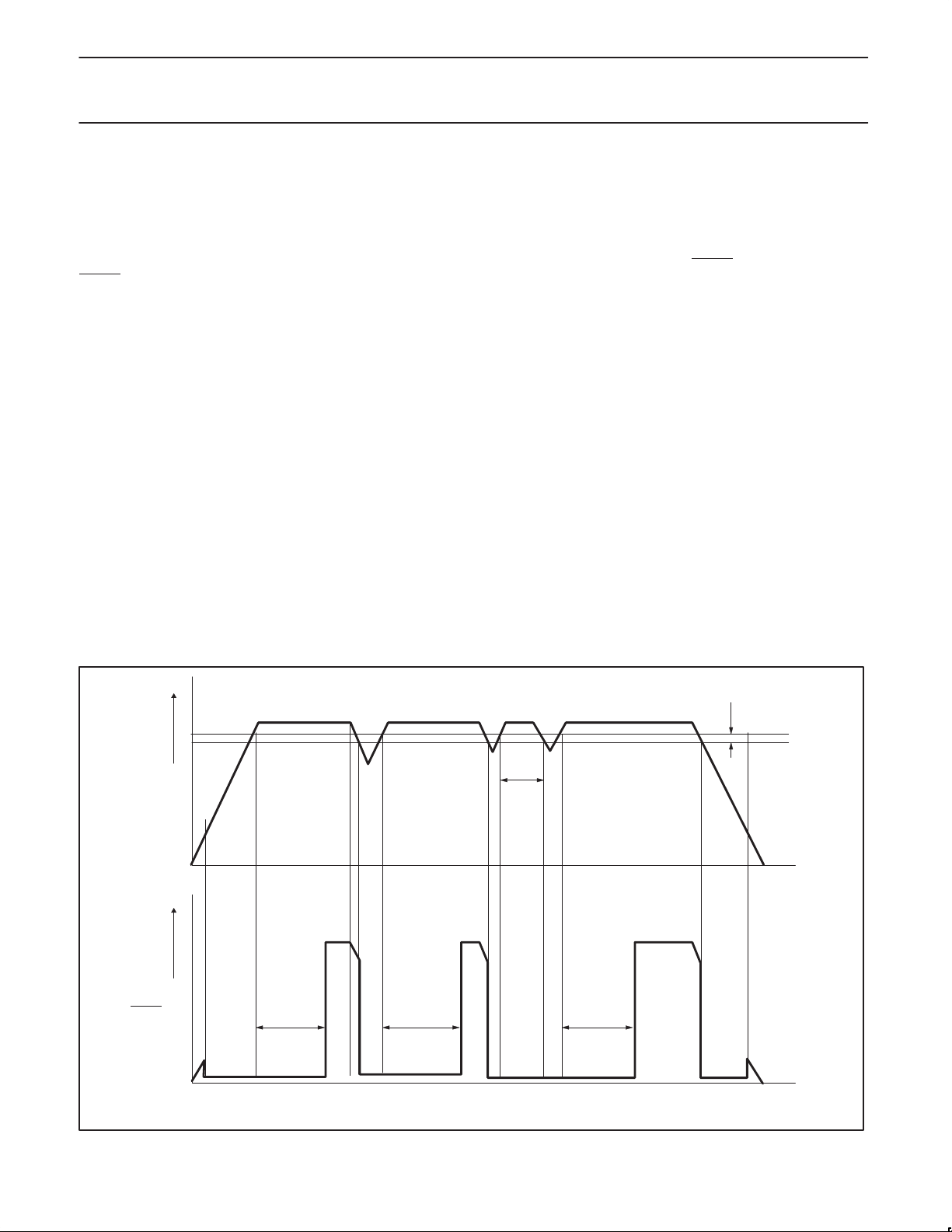
TIMING DIAGRAM
The timing diagram in Figure 23 depicts the operation of the device.
Letters A–N on the TIME axis indicates specific events.
A: At “A”, V
increases but abruptly decreases when V
begins to increase. Also the V
CC
voltage initially
OUT
reaches the level
CC
(approximately 0.65 V) that activates the internal bias circuitry and
RESET is asserted.
B: At “B”, V
delay time, t
operating level. The V
C: At “C”, V
instant, the IC releases the hold on the V
then goes HIGH (assuming the reset pull-up resistor R
connected to V
reaches the threshold level of VSH. At this point the
CC
is initiated while VCC rises above VSH to its normal
PLH
is above VSL and the delay time elapses. At this
CC
CC
voltage remains in a low voltage state.
OUT
reset. The reset output
OUT
PU
is
). In a microprocessor based system these events
release the reset from the microprocessor, allowing the
microprocessor to function normally.
D-E: At “D”, V
begins to fall, causing V
CC
to follow. V
OUT
CC
continues to fall until the VSL undervoltage detection threshold is
reached at “E”. This causes a reset signal to be generated (V
OUT
goes LOW).
E-F: Between “E” and “F”, V
continues to fall and then starts
CC
rising.
F: At “F”, V
rises to the VSH level. Once again, the device
CC
initiates the delay timer.
F-G: V
(t
PLH
V
OUT
rises above VSH and returns to normal. At “G”, the delay
CC
) times out and once again, then it releases the hold on the
reset.
G-H: At “G”, V
causing V
OUT
no reset signal will be generated.
H: At event “H”, V
threshold is reached. At this level, a RESET
V
goes LOW.
OUT
H-I: Between “H” and “I”, V
rise rising. V
again initiated.
I-J: Between “I” and “J”, V
then falls back to V
reasserted before the delay time has elapsed. The time between “I”
and “J” is less than t
released and the reset output remains LOW.
K–L: Between “K” and “L”, V
operating level causing the reset delay to be initiated at “K” and the
reset to be released at “L”.
M: At “M”, V
Reset goes LOW).
N: At “N”, the VCC voltage has decreased until normal internal
circuit bias is unable to maintain a V
rise to less than 0.65 V. As V
also decreases to zero.
is above the upper threshold and begins to fall,
CC
to follow it. As long as VCC remains above the VSH,
falls until the VSL undervoltage detection
CC
signal is generated and
continues to fall and then starts to
rises to the VSH level at “I”, where the delay time is
CC
SL
falls to VSL where the reset is asserted (V
CC
CC
rises above VSH to VCC normal and
CC
level at “J”. At “J”, the reset signal is
(reset delay time). Thus, the reset is not
PLH
rises again back to normal
CC
reset. As a result, VCC may
OUT
decreases further, the V
CC
OUT
OUT
reset
V
CC
V
OUT
(RESET
V
V
)
ABCDEF GHI
t
PLH
t
PLH
Figure 23. Timing diagram.
< t
PLH
t
PLH
JK L M N
V
hys
V
SH
V
SL
SL01606
2002 Mar 25
10
Page 11
Philips Semiconductors Product data
NE56632-XXActive-LOW system reset with adjustable delay time
APPLICATION INFORMATION
A typical application circuit for the NE56632-XX is shown in
Figure 24. Note that a pull-up resistor, R
is necessary since the
PU
output is an open collector. The value of RPU is calculated by the
following expression.
R
≥ (VCC – V
PU
RESET
) / I
OL
where:
VCC = V
V
RESET
= 5 mA; minimum output current at T
I
OL
– 0.05 V (for a 3 V reset this is 2.905 V)
S(min)
= 0.4 V (this is V
OL(max)
)
amb
= 25 °C
Substituting these values into the expression and calculating, finds
R
should be greater than or equal to 510 Ω. To ensure that the
PU
Active-LOW level is sufficient, a value of 4.7 kΩ is chosen in the test
and application examples.
TO V
CC
R
PU
TO RESET
TERMINAL
OF CPU
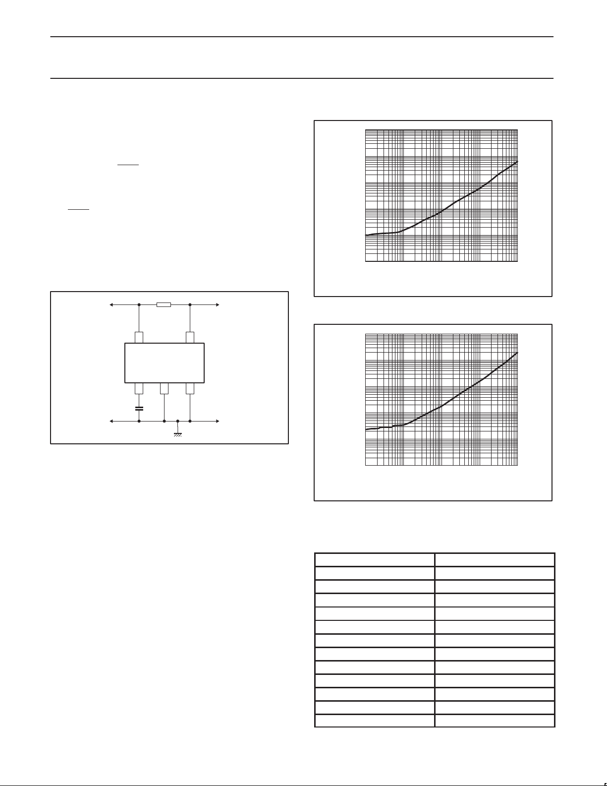
1.0E+00
1.0E–01
1.0E–02
(s)
PLH
t
1.0E–03
1.0E–04
1.0E–05
1.0E+00 1.0E+04
Figure 25. NE56632-20 CD versus t
1.0E+01 1.0E+02 1.0E+03
CD (pF)
PLH
SL01611
characteristics.
45
NE56632-XX
123
C
D
SL01605
Figure 24. Typical application.
Figure 25 (NE56632-20 C
(NE56632-44 C
versus t
D
versus t
D
) show how t
PLH
) and Figure 26
PLH
PHL
, the “H” transmission
delay or reset release delay time varies as a function of the external
delay capacitance, C
. From Figure 26, typical range of the delay
D
capacitance is 1 pF to 10 nF which yields typical delays from 200 µs
to 200 ms.
The following formula can be used to find the approximate delay
time based on external delay capacitance, C
and the delay time
D
coefficient, d shown in Table 2.
(ms) ≈ CD (µF) × d
t
PLH
For example, a NE56632-44 using an external capacitor,
C
= 1 nF = 1000 pF yields:
D
(ms) ≈ (1 × 10⁻³) (1.85 × 10⁴) ≈ 18.5 ms
t
PLH
Compare this to the value of t
≈ 17 ms for CD = 1000 pF that is
PLH
extracted from Figure 26.
1.0E+00
1.0E–01
1.0E–02
(s)
PLH
t
1.0E–03
1.0E–04
1.0E–05
1.0E+00 1.0E+04
1.0E+01 1.0E+02 1.0E+03
CD (pF)
Figure 26. NE56632-44 CD versus t
Table 2. Delay time coefficient
Device d
NE56632–46 1.95 × 10
NE56632–45 1.90 × 10
NE56632–44 1.85 × 10
NE56632–43 1.80 × 10
NE56632–42 1.75 × 10
NE56632–31 1.20 × 10
NE56632–30 1.15 × 10
NE56632–29 1.10 × 10
NE56632–28 1.05 × 10
NE56632–27 1.00 × 10
NE56632–20 0.65 × 10
NE56632–19 0.60 × 10
characteristics.
PLH
SL01612
4
4
4
4
4
4
4
4
4
4
4
4
2002 Mar 25
11
Page 12
Philips Semiconductors Product data
NE56632-XXActive-LOW system reset with adjustable delay time
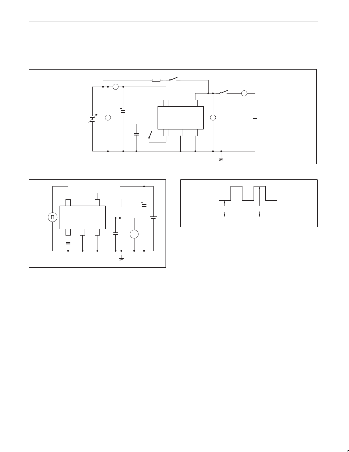
TEST CIRCUITS
S1
R
L
INPUT
PULSE
V
CC1
NE56632-XX
123
C
D
45
V1
100 pF
A1
45
10 µF
/10 V
NE56632-XX
C
S3
D
123
S2
V2
A2
V
CC2
SL01608
Figure 27. Test circuit 1.
R
L
10 µF
/10 V
C
L
CRT
5.0 V
V
– 0.4 V
S(typ)
Figure 29. Input pulse.
V
S(typ)
+ 0.4 V
0V
SL01610
NOTES:
A = DC amperemeter
SL01609
V = DC voltmeter
CRT = oscilloscope
Figure 28. Test circuit 2.
2002 Mar 25
12
Page 13

Philips Semiconductors Product data
NE56632-XXActive-LOW system reset with adjustable delay time
PACKING METHOD
The NE56632-XX is packed in reels, as shown in Figure 30.
GUARD
BAND
BARCODE
LABEL
BOX
TAPE
REEL
ASSEMBLY
Figure 30. Tape and reel packing method.
TAPE DETAIL
COVER TAPE
CARRIER TAPE
SL01305
2002 Mar 25
13
Page 14

Philips Semiconductors Product data
NE56632-XXActive-LOW system reset with adjustable delay time
SOT23-5: plastic small outline package; 5 leads; body width 1.5 mm
2002 Mar 25
1.35
1.2
1.0
0.025
0.55
0.41
0.22
0.08
3.00
2.70
1.70
1.50
14
0.55
0.35
Page 15

Philips Semiconductors Product data
NE56632-XXActive-LOW system reset with adjustable delay time
NOTES
2002 Mar 25
15
Page 16

Philips Semiconductors Product data
NE56632-XXActive-LOW system reset with adjustable delay time
Data sheet status
Product
Data sheet status
Objective data
Preliminary data
Product data
[1] Please consult the most recently issued data sheet before initiating or completing a design.
[2] The product status of the device(s) described in this data sheet may have changed since this data sheet was published. The latest information is available on the Internet at URL
http://www.semiconductors.philips.com.
[1]
status
Development
Qualification
Production
[2]
Definitions
Short-form specification — The data in a short-form specification is extracted from a full data sheet with the same type number and title. For
detailed information see the relevant data sheet or data handbook.
Limiting values definition — Limiting values given are in accordance with the Absolute Maximum Rating System (IEC 60134). Stress above one
or more of the limiting values may cause permanent damage to the device. These are stress ratings only and operation of the device at these or
at any other conditions above those given in the Characteristics sections of the specification is not implied. Exposure to limiting values for extended
periods may affect device reliability.
Application information — Applications that are described herein for any of these products are for illustrative purposes only. Philips
Semiconductors make no representation or warranty that such applications will be suitable for the specified use without further testing or
modification.
Disclaimers
Life support — These products are not designed for use in life support appliances, devices or systems where malfunction of these products can
reasonably be expected to result in personal injury . Philips Semiconductors customers using or selling these products for use in such applications
do so at their own risk and agree to fully indemnify Philips Semiconductors for any damages resulting from such application.
Right to make changes — Philips Semiconductors reserves the right to make changes, without notice, in the products, including circuits, standard
cells, and/or software, described or contained herein in order to improve design and/or performance. Philips Semiconductors assumes no
responsibility or liability for the use of any of these products, conveys no license or title under any patent, copyright, or mask work right to these
products, and makes no representations or warranties that these products are free from patent, copyright, or mask work right infringement, unless
otherwise specified.
Contact information
For additional information please visit
http://www.semiconductors.philips.com . Fax: +31 40 27 24825
For sales offices addresses send e-mail to:
sales.addresses@www.semiconductors.philips.com.
Definitions
This data sheet contains data from the objective specification for product development.
Philips Semiconductors reserves the right to change the specification in any manner without notice.
This data sheet contains data from the preliminary specification. Supplementary data will be
published at a later date. Philips Semiconductors reserves the right to change the specification
without notice, in order to improve the design and supply the best possible product.
This data sheet contains data from the product specification. Philips Semiconductors reserves the
right to make changes at any time in order to improve the design, manufacturing and supply.
Changes will be communicated according to the Customer Product/Process Change Notification
(CPCN) procedure SNW-SQ-650A.
Koninklijke Philips Electronics N.V. 2002
All rights reserved. Printed in U.S.A.
Date of release: 08-02
Document order number: 9397 750 10239
2002 Mar 25
16
 Loading...