

Page 1

INTEGRATED CIRCUITS
NE56604-42
System reset with built-in watchdog timer
Product data
Supersedes data of 2001 Jun 19
File under Integrated Circuits, Standard Analog
2001 Aug 22
Page 2

Philips Semiconductors Product data
TYPE NUMBER
NE56604-42System reset with built-in watchdog timer
GENERAL DESCRIPTION
The NE56604-42 is designed to generate a reset signal at a
threshold voltage of 4.2 V for a variety of microprocessor and logic
systems. Accurate reset signals are generated during momentary
power interruptions, or whenever power supply voltages sag to
intolerable levels. The NE56604-42 has a built-in Watchdog Timer to
monitor the microprocessor and ensure it is operating properly. Any
abnormal system operations due to microprocessor malfunctions
are terminated by a system reset generated by the watchdog. The
NE56604-42 has a watchdog monitoring time of 100 ms (typical).
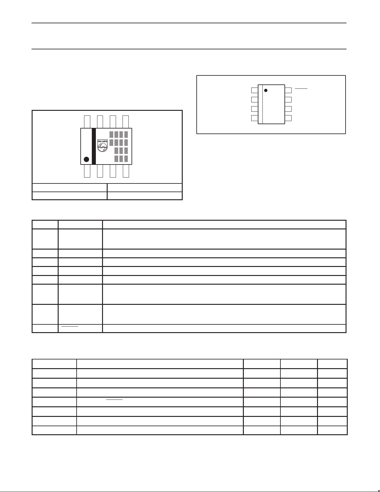
The NE56604-42 is offered in the SO8 surface mount package.
FEATURES
•Both positive and negative logic reset output signals are available
•Accurate threshold detection
•Internal power-on reset delay
•Internal watchdog timer programmable with external resistor
•Watchdog monitoring time of 100 ms (typical)
•Reset assertion with V
•Few external components required.
down to 0.8 VDC (typical)
CC
APPLICA TIONS
•Microcomputer systems
•Logic systems.
SIMPLIFIED SYSTEM DIAGRAM
V
CC
5
V
C
R
S
7
R
R
CT
R
6
CT
NE56604-42
RESET
GENERATOR
V
REF
4
GND
PROGRAMMABLE
WATCHDOG TIMER
1
C
T
Figure 1. Simplified system diagram.
8
2
3
RESET
RESET
CLK
LOGIC
SYSTEM
RESET
RESET
CLK
GND
SL01281
ORDERING INFORMATION
PACKAGE
NAME DESCRIPTION
TEMPERATURE
RANGE
NE56604-42D SO8 plastic small outline package; 8 leads; body width 3.9 mm –20 to +70 °C
2001 Aug 22 853–2250 26949
2
Page 3
Philips Semiconductors Product data
NE56604-42System reset with built-in watchdog timer
Part number marking
PIN CONFIGURATION
The package is marked with a four letter code in the first line to the
right of the logo. The first three letters designate the product. The
fourth letter, represented by ‘x’, is a date tracking code. The
remaining two or three lines of characters are internal manufacturing
codes.
5
6
7
8
2
1
3
4
Part number Marking
NE56604-42 A A D x
PIN DESCRIPTION
PIN SYMBOL DESCRIPTION
1 C
T
2 RESET Reset HIGH output pin.
3 CLK Clock input pin from logic system for watchdog timer.
4 GND Circuit ground.
5 V
6 R
7 V
CC
CT
S
8 RESET Reset LOW output pin.
t
, t
WDM
t
WDM
Diagram) for definition of t
, tPR adjustment pin.
WDR
, t
, tPR times are dependent on the value of external CT capacitor used. See Figure 20 (Timing
WDR
WDM
, t
WDR
, tPR times.
Power supply pin for circuit.
Watchdog timer control and program pin.
Serves to ENABLE the watchdog function when connected to pull-up resistor (RCT) to VCC, and DISABLE
the watchdog when connected to ground. Used in conjunction with C
Detection threshold adjustment pin.
The detection threshold can be increased by connecting this pin to VCC with a pull-up resistor. The detection
threshold can be decreased by connecting this pin to ground with a pull-down resistor.
TOP VIEW
8
7
6
5
SL01280
RESET
CLK
GND
1
C
T
2
SO8
3
4
Figure 2. Pin configuration.
pin to program t
T
RESET
V
S
R
CT
V
CC
WDM
time.
MAXIMUM RATINGS
SYMBOL PARAMETER MIN. MAX. UNIT
V
CC
V
VS
V
CLK
V
OH
T
oper
T
stg
P Power dissipation – 250 mW
2001 Aug 22
Power supply voltage –0.3 10 V
VS pin voltage –0.3 10 V
CLK pin voltage –0.3 10 V
RESET and RESET pin voltage –0.3 10 V
Operating temperature –20 70 °C
Storage temperature –40 125 °C
3
Page 4

Philips Semiconductors Product data
NE56604-42System reset with built-in watchdog timer
DC ELECTRICAL CHARACTERISTICS
Characteristics measured with VCC = 5.0 V, and T
See Figure 26 (Test circuit 1) for test configuration used for DC parameters.
SYMBOL PARAMETER CONDITIONS MIN. TYP. MAX. UNIT
I
CC
V
SL
V
SH
∆VS/∆T
V
hys
V
TH
I
IH
I
IL
V
OH1
V
OH2
V
OL1
V
OL2
V
OL3
V
OL4
I
OL1
I
OL2
I
CT1
I
CT2
V
CCL1
V
CCL2
Supply current during watchdog timer
operation
Reset detection threshold
Temperature coefficient of reset threshold –20 °C ≤ T
amb
Threshold hysteresis V
CLK input threshold 0.8 1.2 2.0 V
CLK input current, HIGH-level V
CLK input current, LOW-level V
Output voltage, HIGH-level
Output voltage, LOW-level
Output sink current
CT charge current (Note 1)
Supply voltage to assert reset operation
NOTE:
1. I
source current is determined by the value of the RCT pull-up resistor to VCC.
CT
= 25 °C, unless otherwise specified.
amb
VS = open; VCC = falling 4.05 4.20 4.35 V
VS = open; VCC = rising 4.15 4.30 4.45 V
amb
= VSH (rising VCC) – V
hys
(falling VCC)
= 5.0 V – 0 1.0 µA
CLK
= 0 V –20 –10 –3.0 µA
CLK
I
= –5.0 µA; VS = open 4.5 4.8 – V
RESET
I
current = –5.0 mA; VS = 0 V 4.5 4.8 – V
RESET
I
= 3.0 mA; VS = 0 V – 0.2 0.4 V
RESET
I
= 10 mA; VS = 0 V – 0.3 0.5 V
RESET
I
= 0.5 mA; VS = open – 0.2 0.4 V
RESET
I
= 1.0 mA; VS = open – 0.3 0.5 V
RESET
V
= 1.0 V; VS = 0 V 10 16 – mA
RESET
V
= 1.0 V; VS = open 1.0 2.0 – mA
RESET
VCT = 1.0 V; RCT = open during
watchdog operation
VCT = 1.0 V;
during power-on reset operation
V
= 0.4 V; I
RESET
V
RESET
1 MΩ resistor (pin 2 to GND)
RESET
= VCC – 0.1 V;
– 0.7 1.0 mA
≤ 70 °C – ±0.01 – %/°C
SL
50 100 150 mV
–0.8 –1.2 –2.4 µA
–0.8 –1.2 –2.4 µA
= 0.2 mA – 0.8 1.0 V
– 0.8 1.0 V
2001 Aug 22
4
Page 5
Philips Semiconductors Product data
NE56604-42System reset with built-in watchdog timer
AC ELECTRICAL CHARACTERISTICS
Characteristics measured with VCC = 5.0 V, and T
See Figure 27 (Test circuit 2) for test configuration used for AC parameters.
SYMBOL PARAMETER CONDITIONS MIN. TYP. MAX. UNIT
t
P1
t
CLKW
t
CLK
t
WDM
t
WDR
t
PR
t
PD1
t
PD2
t
R1
t
R2
t
F1
t
F2
Minimum power supply pulse width for
detection
Clock input pulse width 3.0 – – µs
Clock input cycle 20 – – µs
Watchdog monitoring time (Notes 1, 6) CT = 0.1 µF; RCT = open 50 100 150 ms
Watchdog reset time (Notes 2, 6) CT = 0.1 µF 1.0 2.0 3.0 ms
Power-on reset delay time (Notes 3, 6) VCC = rising from 0 V; CT = 0.1 µF 50 100 150 ms
Reset propagation delay time (Note 4)
Reset rise time (Note 5)
Reset fall time (Note 5)
NOTES:
1. ‘Watchdog monitoring time’ is the duration from the last pulse (negative-going edge) of the timer clear clock pulse until reset output pulse
occurs (see Figure 20). A reset signal is output if a clock pulse is not input during this time. Watchdog monitoring time can be modified by
changing the value of the R
2. ‘Watchdog reset time’ is the reset pulse width (see Figure 20).
pull-up resistor. Monitoring time adjustments are shown in Figure 25.
CT
3. ‘Power-on reset delay time’ is the duration measured from the time V
release is experienced (RESET
output HIGH; RESET output LOW).
4. ‘Reset response time’ is the duration from when the supply voltage sags below the lower detection threshold (V
output LOW, RESET output HIGH).
5. Reset rise and fall times are measured at 10% and 90% output levels.
6. Watchdog monitoring time (t
varying the C
to 10 µF.
capacitance. The times can be approximated by applying the following formula. The recommended range for CT is 0.001 µF
T
), watchdog reset time (t
WDM
Formula 1. Calculation for approximate t
(ms) ≈ 1000 × CT (µF)
t
PR
t
(ms) ≈ 1000 × CT (µF)
WDM
t
(ms) ≈ 20 × CT (µF)
WDR
Example: When CT = 0.1 µF and RCT = open:
t
≈ 100 ms
PR
t
≈ 100 ms
WDM
t
≈ 2.0 ms
WDR
= 25 °C, unless otherwise specified.
amb
4.0 V ≤ negative-going VCC pulse ≤ 5.0 V 8.0 – – µs
RESET: RL1 = 2.2 kΩ; CL1 = 100 pF – 2.0 10 µs
RESET: RL2 = 10 kΩ; CL2 = 20 pF – 3.0 10 µs
RESET: RL1 = 2.2 kΩ; CL1 = 100 pF – 1.0 1.5 µs
RESET: RL2 = 10 kΩ; CL2 = 20 pF – 1.0 1.5 µs
RESET: RL1 = 2.2 kΩ; CL1 = 100 pF – 0.1 0.5 µs
RESET: RL2 = 10 kΩ; CL2 = 20 pF – 0.5 1.0 µs
CC
), and power-on reset delay time (tPR) during power-on can be modified by
WDR
, t
PR
WDM
, and t
WDR
values:
exceeds the upper detection threshold (VSH) and power-on reset
) and reset occurs (RESET
SL
2001 Aug 22
5
Page 6

Philips Semiconductors Product data
NE56604-42System reset with built-in watchdog timer
TYPICAL PERFORMANCE CURVES
1.4
T
= 35 °C
amb
1.2
1.0
0.8
0.6
0.4
POWER SUPPLY CURRENT (mA)
CC
0.2
I
0
0 1.0 2.0 3.0 4.0 5.0 6.0 7.0 8.0 9.0 10.0
WITHOUT
CLOCK SIGNALS
TO WATCHDOG
WITH
CLOCK SIGNALS
TO WATCHDOG
VCC, POWER SUPPLY VOLTAGE (V)
Figure 3. Power supply current vs. voltage.
6.0
RESET PULL-UP R = 2.2 kΩ
5.0
4.0
3.0
2.0
, RESET OUTPUT VOLTAGE (V)
RST
1.0
V
0
0 1.0 2.0 3.0 4.0 5.0 6.0
T
= –25 °C
amb
T
= 25 °C
amb
T
= 75 °C
amb
VCC POWER SUPPLY VOLTAGE (V)
V
SL
V
OL
Figure 5. RESET output voltage vs. supply voltage.
6.0
RESET PULL-UP R = 10 kΩ
SL01303
5.0
4.0
3.0
2.0
, RESET OUTPUT VOLTAGE (V)
1.0
RST
V
0
0 1.0 2.0 3.0 4.0 5.0 6.0 7.0 8.0
VCC, POWER SUPPLY VOLTAGE (V)
T
= –25 °C, 25 °C, 75 °C
amb
V
SL
V
SH
V
OL
SL01304
Figure 4. RESET output voltage vs. supply voltage.
4.5
VCC = RISING (VSH)
VCC = FALLING (VSL)
4.4
V
4.3
V
SH
4.2
, DETECTION THRESHOLD (V)
SH
4.1
, V
SL
V
4.0
–40 –20 0 20 40 60 80 100
T
, AMBIENT TEMPERATURE (°C)
amb
SL01302
SH
V
SL
SL01301
Figure 6. Detection threshold vs. temperature.
600
500
400
300
200
100
, RESET OUTPUT SATURATION (mV)
OL
V
0
0 –0.6 –0.8 –1.0 –1.2 –1.4 –1.6 –1.8
Figure 7. RESET saturation vs. sink current.
2001 Aug 22
VCC = 5.0 V
RESET PULL-UP R = 10 kΩ
T
amb
–0.2 –0.4
IOL, RESET OUTPUT SINK CURRENT (mA)
= 25 °C
T
amb
= 75 °C
T
amb
= –25 °C
SL01300
600
500
400
300
200
100
, RESET OUTPUT SATURATION (mV)
OL
V
0
0 –6 –8 –10 –12 –14 –16 –18
VCC = 5.0 V
RESET
PULL-UP R = 2.2 kΩ
T
= 75 °C
amb
–2 –4
IOL, RESET OUTPUT SINK CURRENT (mA)
T
amb
T
= –25 °C
amb
= 25 °C
SL01299
Figure 8. RESET saturation vs. sink current.
6
Page 7

Philips Semiconductors Product data
NE56604-42System reset with built-in watchdog timer
5.2
5.0
4.8
4.6
4.4
, RESET HIGH LEVEL OUTPUT (V)
4.2
OM
V
4.0
0 –2 –4 –6 –8 –10 –12 –14 –16 –18
IOM, RESET HIGH OUTPUT LEAKAGE CURRENT (µA)
VCC = 5.0 V
T
amb
Figure 9. RESET HIGH-level voltage vs. current.
140
VCC = 5.0 V
CT = 0.1 µF
= Open
R
CT
120
100
= 25 °C
SL01298
5.0
4.8
VCC = 5.0 V
4.6
T
= 25 °C
amb
4.4
4.2
4.0
, RESET HIGH LEVEL OUTPUT (V)
OM
3.8
V
3.6
0 –2.0 –4.0 –6.0 –8.0 –10 –16–14–12
IOM, RESET HIGH OUTPUT LEAKAGE CURRENT (µA)
Figure 10. RESET HIGH-level voltage vs. current.
140
VCC = 5.0 V
CT = 0.1 µF
= Open
R
CT
120
100
SL01297
80
, POWER-ON RESET HOLD (ms)
PR
t
60
–40 –20
T
, AMBIENT TEMPERATURE (5C)
amb
Figure 11. Power–on reset hold time vs. temperature.
3.0
VCC = 5.0 V
CT = 0.1 µF
2.5
2.0
1.5
, WATCHDOG RESET (ms)
WDR
t
1.0
040
, AMBIENT TEMPERATURE (°C)
T
amb
Figure 13. Watchdog reset time vs. temperature.
100806040200
SL01296
SL01294
80
, WATCHDOG MONIT ORING (ms)
WDM
t
60
–40 –20
T
, AMBIENT TEMPERATURE (5C)
amb
100806040200
SL01295
Figure 12. Watchdog monitoring time vs. temperature.
100
RCT = 5 MΩ
VCC = 5.0V
CT = 0.1 µF
10
RCT = 100 kΩ
, WATCHDOG MONIT ORING (ms)
WDM
t
100806020–20–40
1
0 40 100806020–20–40
T
, AMBIENT TEMPERATURE (°C)
amb
SL01308
Figure 14. Watchdog monitoring time vs. temperature.
2001 Aug 22
7
Page 8

Philips Semiconductors Product data
NE56604-42System reset with built-in watchdog timer
4
10
VCC = 5.0 V
T
= 25 °C
amb
3
10
2
10
10
, POWER-ON RESET HOLD (ms)
PR
t
1.0
–3
10
–2
10
–1
10
CT, CAPACITANCE (µF)
Figure 15. Power-on reset hold time vs. CT.
4
10
VCC = 5.0 V
T
= 25 °C
amb
3
10
2
10
10
, WATCHDOG MONIT ORING (ms)
WDM
t
1.0
–3
10
–2
10
–1
10
CT, CAPACITANCE (µF)
Figure 17. Watchdog reset time vs. CT.
1.0 10
SL01290
1.0 10
SL01307
2
10
VCC = 5.0 V
T
= 25 °C
amb
10
1.0
–1
10
, WATCHDOG RESET (ms)
WDR
t
–2
10
–3
10
–2
10
–1
10
CT, CAPACITANCE (µF)
Figure 16. Watchdog reset time vs. CT.
5
10
VCC = 5.0 V
T
= 25 °C
amb
4
10
3
10
2
10
10
1.0
, WATCHDOG MONIT ORING (ms)
–1
10
WDM
t
–2
10
–3
10
–2
10
C
–1
10
, CAPACITANCE (µF)
T
Figure 18. Watchdog monitoring time vs. CT.
1.0 10
SL01291
RCT = OPEN
R
= 2.2 MΩ
CT
= 1.0 MΩ
R
CT
R
= 470 kΩ
CT
= 200 kΩ
R
CT
1.0 10
SL01309
2001 Aug 22
8
Page 9

Philips Semiconductors Product data
NE56604-42System reset with built-in watchdog timer
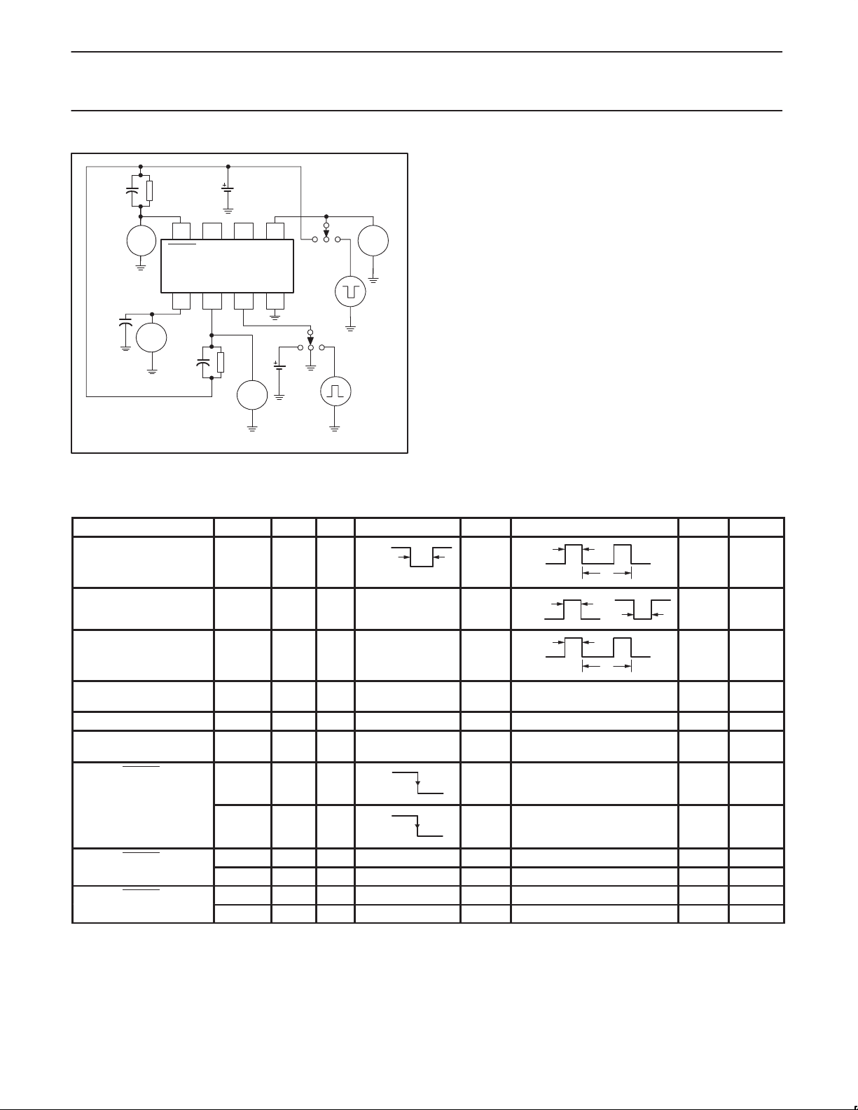
TECHNICAL DESCRIPTION
General discussion
The NE56604-42 combines a watchdog timer and an undervoltage
reset function in a single SO8 surface mount package. This provides
a space-saving solution for maintaining proper operation of typical
5.0 volt microprocessor-based logic systems. Either function, or
both, can force the microprocessor into a reset.
While the watchdog monitors the microprocessor operation, the
undervoltage reset monitors the supply voltage to the
microprocessor. If the microprocessor clock signal ceases or
becomes erratic, the NE56604-42 outputs a reset signal to the
microprocessor. If the microprocessor supply voltage sags to
4.2 volts or less, the NE56604-42 outputs a reset signal for the
duration of the supply voltage deficiency. The undervoltage reset
signal allows the microprocessor to shut down in an orderly manner
to avoid system corruption. In addition to a single reset output, the
NE56604-42 has complementary RESET
system use. The undervoltage detection threshold incorporates
hysteresis to prevent generating erratic resets.
V
CC
5
and RESET outputs for
R
CT
6
R
CT
The watchdog timer requires a pulse input. Normally this signal
comes from the system microprocessor’s clock. For operation, an
external resistor (R
external capacitor (C
capacitor is used for C
) must be connected from Pin 6 to VCC and an
CT
) from Pin 1 to ground. Normally a 0.1 µF
T
. The external RCT resistor and CT capacitor
T
establish the required minimum frequency of watchdog input signal
for the device to not output a reset signal. The RCT resistor
establishes, in part, the rate of charge of the C
absence of a watchdog input pulse, the C
capacitor. In the
T
capacitor charges to the
T
0.2 volt threshold of the internal comparator, causing a reset signal
to be output. If microprocessor clock signals are received within the
required interval, no watchdog reset signal will be output. The
watchdog function can be disabled by grounding Pin 6 without
affecting the undervoltage detection function.
Although the temperature coefficient of detection threshold is
specified over a temperature of –20 °C to +70 °C, the device will
support operation in excess of this temperature range. See the
supporting curves for performance over the full temperature range of
–40 °C to +85 °C. Some degradation in performance will be
experienced at the temperature extremes and the system designer
should take this into account.
0.1 V
R
R
54 kΩ
7
C
26 kΩ
3
58 kΩ
R
PULSE
GENERATOR
Q
1.2 µA
S
Q
R
R
R
0.2 V
1C
T
S
R
Q
S
R
4
GND
R
47 kΩ
12 µA
2
RESET
R
8
RESET
SL01310
R
Figure 19. Functional diagram.
2001 Aug 22
9
Page 10
Philips Semiconductors Product data
NE56604-42System reset with built-in watchdog timer
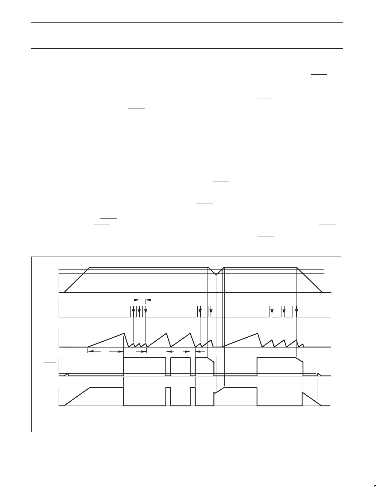
Timing diagram
The timing diagram shown in Figure 20 depicts the operation of the
device. Letters indicate events on the TIME axis.
A: At start-up ‘A’, the V
the RESET
voltage initially rises, but then abruptly returns to a LOW
state. This is due to V
activates the internal bias circuitry, asserting RESET
B: Just before ‘B’, the C
by, and coincident to, V
and RESET voltages begin to rise. Also
CC
reaching the level (RESET 0.8 V) that
CC
.
voltage starts to ramp up. This is caused
T
reaching the threshold level of VSH. At
CC
this level the device is in full operation. The RESET output continues
to rise as V
C: At ‘C’, V
rises above VSH. This is normal.
CC
is above the undervoltage detect threshold, and C
CC
T
has ramped up to its upper detect level. At this point, the device
removes the hold on the resets. RESET
goes HIGH while RESET
goes LOW. Also, an internal ramp discharge transistor activates,
discharging C
.
T
In a microprocessor-based system these events remove the reset
from the microprocessor, allowing it to function normally. The system
must send clock signals to the Watchdog Timer often enough to
prevent C
signals from being generated. Each clock signal discharges C
from ramping up to the CT threshold, to prevent reset
T
.
T
C–D: Midway between ‘C’ and ‘D’, the CLK signals cease allowing
the C
voltage to ramp up to its RESET threshold at ‘D’. At this time,
T
reset signals are generated (RESET
HIGH). The device attempts to come out of reset as the C
goes LOW; RESET goes
voltage
T
is discharged and finally does come out of reset when CLK signals
are re-established after two attempts of C
.
T
E–F: Immediately before ‘E’, falling V
to sag. CLK signals are still being received, C
operating range, and reset signals are not output. V
sag until the V
undervoltage threshold is reached. At that time,
SL
reset signals are generated (RESET
causes the RESET signal
CC
is within normal
T
continues to
CC
goes LOW; RESET goes
HIGH).
At ‘E’, V
However, C
starts to rise, and the RESET voltage rises with VCC.
CC
voltage does not start to ramp up until ‘F’, when V
T
CC
reaches the VSH upper threshold.
G: The reset outputs are released at ‘G’ when C
reaches the
T
upper threshold level again. After ‘G’, normal CLK signals are
received, but at a lower frequency than those following event ‘C’.
The frequency is above the minimum frequency required to keep the
device from outputting reset signals.
G–H: At ‘H’, V
no reset signals are output. At event ‘H’, the V
causing RESET
J: At event ‘J’, V
is normal, CLK signals are being received, and
CC
starts falling,
CC
to also fall.
sags to the point where the VSL undervoltage
CC
threshold point is reached, and at that level reset signals are output
(RESET
to a LOW state, and RESET to a HIGH state). As the V
CC
voltage falls lower, the RESET voltage falls lower.
K: At event ‘K’, the V
normal internal circuit bias is no longer able to maintain a RESET
voltage has deteriorated to a level where
CC
,
and as a result may exhibit a slight rise to something less than 0.8 V .
As V
decays even further, RESET also decreases to zero.
CC
V
V
V
CLK
C
Tthresh
RESET
0.8 V
RESET
SH
SL
CC
t
CLK
C
T
t
PR
AB C D EF G HJK
t
WDM
TIME
t
WDR
Figure 20. Timing diagram.
SL01283
2001 Aug 22
10
Page 11
Philips Semiconductors Product data
NE56604-42System reset with built-in watchdog timer
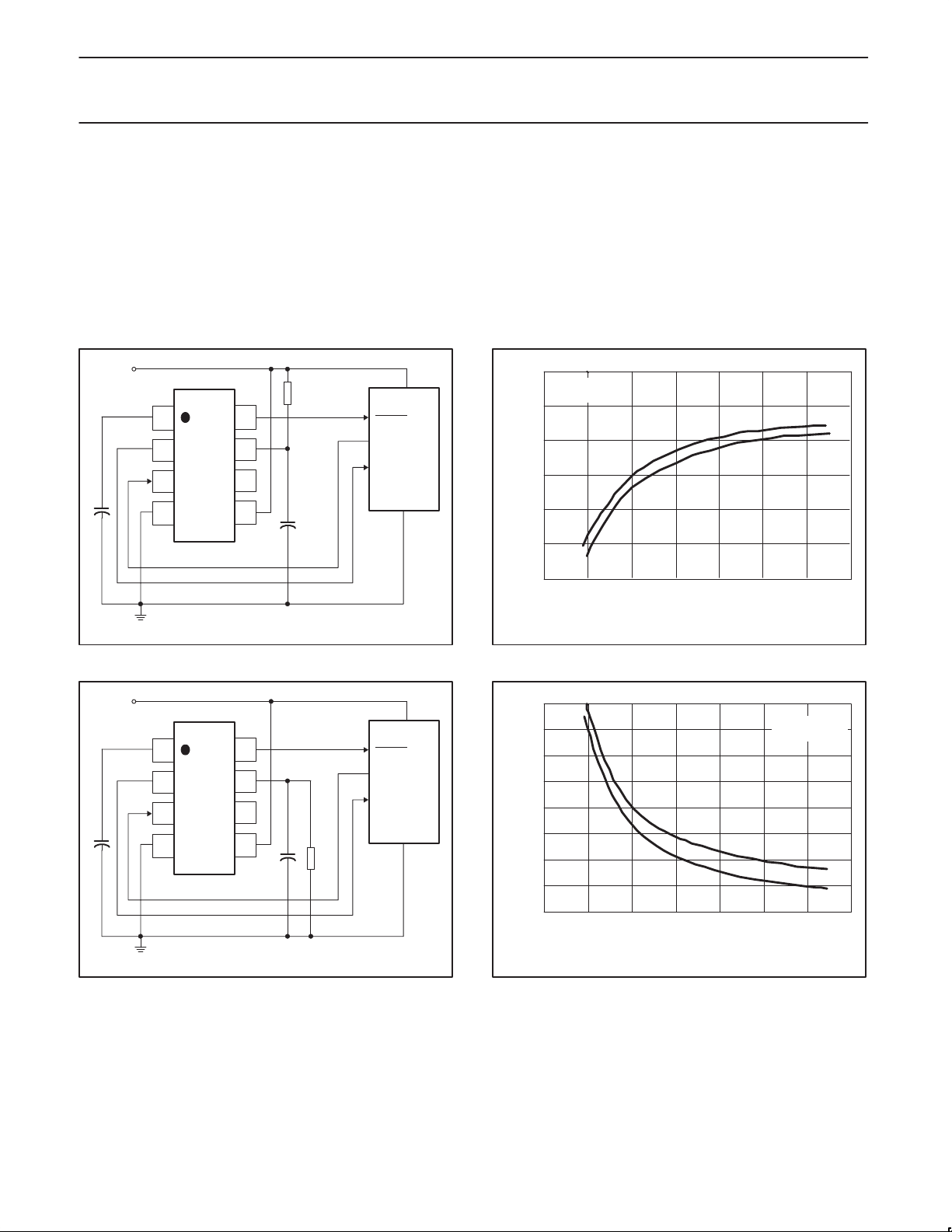
Application information
The watchdog timer’s external component values are critical to its
performance.
The detection threshold voltage can be adjusted by externally
influencing the internal divider reference voltage. Figures 21 and 23
show a method to lower and raise the threshold voltage. Figures 22
and 24 show the influence of the pull-down and pull-up resistors on
the threshold voltage. The use of a capacitor (1000 pF or larger)
from Pin 7 to ground is recommended to filter out noise from being
imposed on the threshold voltages.
V
CC
1
2
3
C
T
4
8
7
6
NE56604-42
5
1000 pF
R
1
LOGIC SYSTEM
RESET
CLK
RESET
GND
The Reset Detection Threshold can be decreased by connecting an
external resistor R
Figure 22 to determine the approximate value of R
from Pin 7 to VCC, as shown in Figure 21. See
1
to use.
1
The Reset Detection Threshold can be increased by connecting an
external resistor R
See Figure 24 to determine the approximate value of R
5.0
4.0
3.5
Vs, RESET DETECTION THRESHOLD (V)
3.0
0 100 200 300 400 500 600 700
from Pin 7 to ground, as shown in Figure 23.
2
VCC = 5.0 V
T
= 25 °C
amb
V
SH
V
SL
R1, EXTERNAL PIN 7 TO VCC RESISTOR (kΩ)
to use.
2
Figure 21. Circuit to lower detection threshold.
V
CC
1
2
3
C
T
4
8
7
6
NE56604-42
5
1000 pF
Figure 23. Circuit to raise detection threshold.
LOGIC SYSTEM
R
2
SL01327
RESET
CLK
RESET
SL01328
GND
Figure 22. Reset detection threshold vs. external R1.
5.1
5.0
4.9
4.8
4.7
4.6
4.5
4.4
Vs, RESET DETECTION THRESHOLD (V)
4.3
0 100 200 300 400 500 600 700
, EXTERNAL PIN 7 TO GROUND RESISTOR (kΩ)
R
2
V
V
SL
VCC = 5.0 V
T
amb
SH
Figure 24. Reset detection threshold vs. external R2.
SL01326
= 25 °C
SL01325
2001 Aug 22
11
Page 12

Philips Semiconductors Product data
NE56604-42System reset with built-in watchdog timer
The values of R
(t
), the watchdog reset time (t
WDM
time (t
). See Formula 1 in the AC Electrical Characteristics and
PR
and CT affect the watchdog monitoring time
CT
), and power-on reset delay
WDR
the Timing diagram shown in Figure 20 for parameter definitions.
Also see Figures 11 through 18 for typical time relationship
performance.
The effect of R
temperature for C
on the watchdog timer monitoring time at room
CT
= 0.1 mF is shown in Figure 25.
T
100
CT = 0.1 µF
T
= 25 °C
amb
80
60
40
20
, WATCHDOG MONIT OR TIME (ms)
WDM
t
0
10k 100k 1M 10M 100M
, WATCHDOG TIMER CURRENT RESISTOR (Ω)
R
CT
SL01329
Figure 25. Watchdog monitoring vs. pull-up resistor RCT.
∞
2001 Aug 22
12
Page 13

Philips Semiconductors Product data
NE56604-42System reset with built-in watchdog timer
Parametric testing
DC and AC Characteristics can be tested using the circuits shown in
Figures 26 and 27. Associated switch and power supply settings are
shown in Table 1 and Table 2, respectively.
CLK
V
S
5
S
V
S
CLK
6
A
I
CC
V
CC
SL01284
7
0.1 µF
CC
42
V
O2
2
ABC
S
1
V
O0
CRT
S
2
V
CRT
V
O1
1
V
1.0 MΩ
CT
A
R
S
I
RESET
1000 pF
I
O1
8
VSRCTV
RESET
3
CTRESET CLK GND
A A A
I
CT
S
4
ABC
I
RESET
6 5
7
31
I
I
O2
CRT
CRT
Figure 26. Test Circuit 1 (DC parameters).
Table 1. DC characteristics Test Circuit 1 switch and power supply settings
Parameter Symbol S1S2S3S4S5S6S
Power supply current I
Reset threshold (LOW) (Note 1) V
Reset threshold (HIGH) (Note 2) V
Clock input threshold (Note 3) V
Clock input current (HIGH) I
Clock input current (LOW) I
Reset output voltage (HIGH)
Reset output voltage (LOW)
Reset output sink current
(Note 4)
CT charge current 1 I
CT charge current 2 I
Minimum power supply for
(Note 5)
RESET
Minimum power supply for
RESET (Note 6)
NOTES:
1. Decrease V
2. Increase V
3. Increase the Clock voltage (V
4. Measured with V
5. Increase V
will initially track the V
6. Increase V
from 5.0 V to 4.0 V and note the VCC value when VO1 (observed on CRT1) transitions to an abrupt LOW state.
CC
from 4.0 V to 5.0 V and note the VCC value when VO1 (observed on CRT1) transitions to an abrupt HIGH state.
CC
= 1.0 V.
O0
from 0 V to 2.0 V and note the VCC value when VO1 (observed on CRT1) transitions to an abrupt LOW state. The VO1 value
CC
from 0 V to 2.0 V and note the VCC value when VO2 (observed on CRT2) starts to track the VCC voltage.
CC
voltage increa se until the in ternal circuit bias beco mes active, at which time the VO1 value will return to a LOW state.
CC
B OFF OFF B OFF ON ON 5.0 V 5.0 V 0 V – – I
CC
B OFF OFF B ON ON ON 5.0 to 4.0 V 3.0 V 3.0 V – – VO1, CRT
SL
B OFF OFF B ON ON ON 4.0 to 5.0 V 3.0 V 3.0 V – – VO1, CRT
SH
B OFF OFF B OFF ON ON 5.0 V 0 to 3.0 V 1.0 V – – I
TH
B OFF OFF B OFF ON ON 5.0 V 5.0 V 0 V – – I
TH
B OFF OFF B OFF ON ON 5.0 V 0 V 0 V – – I
TL
V
V
V
V
V
V
V
V
CLK
I
OL1
I
OL2
CT1
CT2
CCL1
CCL2
B OFF ON B ON ON ON 5.0 V 5.0 V 3.0 V –5.0 µA – V
OH1
B ON OFF C ON ON ON 5.0 V 5.0 V 3.0 V – –5.0 µA V
OH2
B ON ON B ON ON ON 5.0 V 5.0 V 3.0 V 3.0 mA – V
OL1
B ON ON B ON ON ON 5.0 V 5.0 V 3.0 V 10 mA – V
OL2
B OFF OFF C ON ON ON 5.0 V 5.0 V 3.0 V – 0.5 mA V
OL3
B OFF OFF C ON ON ON 5.0 V 5.0 V 3.0 V – 1 mA V
OL4
C ON OFF B ON ON ON 5.0 V 5.0 V 3.0 V – – I
A OFF OFF B ON ON ON 5.0 V 5.0 V 3.0 V – – I
B OFF OFF B OFF OFF ON 5.0 V – 1.0 V – – I
B OFF OFF B ON OFF ON 5.0 V – 1.0 V – – I
B OFF ON B ON ON ON 0 to 2.0 V 0 V 0 V – – VO1, V
B ON OFF A ON ON ON 0 to 2.0 V 0 V 0 V – – VO2, V
) from 0 V to 3.0 V and observe the value of V
V
7
CC
when I
CLK
V
CLK
transitions to an abrupt increase.
CLK
VCTI
RESETIRESET
Read
CC
1
1
CLK
CLK
CLK
O1
O2
O1
O1
O2
O2
O1
O2
CT
CT
CC
CC
2001 Aug 22
13
Page 14
Philips Semiconductors Product data
NE56604-42System reset with built-in watchdog timer
R
100 pF
0.1 µF
CRT
CRT
1
2.2 kΩ
8 6 57
RESET
CTRESET CLK GND
CRT
CRT
2
20pF
V
CC
V
R
V
S
R
10 kΩ
CT
CRT
CRT
CC
42 31
V
3
AC
S
AC
B
CLK
S
1
CRT
B
2
V
CLKA
V
CCA
SL01285
CRT
4
Figure 27. Test Circuit 2 (AC parameters).
Table 2. Switch and power supply settings, AC parameters
Parameter Symbol S
VCC pulse width for
detection (Note 1)
Clock input pulse width
(Note 2)
Clock input cycle
(Note 3)
Watchdog monitoring
time
Watchdog reset time t
Power-on reset delay
time
RESET, RESET
propagation delay time
RESET, RESET rise time
RESET, RESET fall time
NOTES:
= 8.0 µs.
1. t
1
2. t
= 3.0 µs.
2
= 20 µs.
3. t
3
t
P1
t
CLKW
t
CLK
t
WDM
WDR
t
PR
t
PD1
t
PD2
t
R1
t
R2
t
F1
t
F2
B to A A – 5.0 V – 5.0 V 1, 2, 3
1
C C
S
2
5.0 V
4.0 V
V
CCA
t
1
A C – 5.0 V
A C – 5.0 V
A A – 5.0 V – 5.0 V 1, 2, 3
A A – 5.0 V – 5.0 V 1, 2, 3
C B
C B
5.0 V
4.0 V
5.0 V
4.0 V
A A – 5.0 V – 5.0 V 1
A A – 5.0 V – 5.0 V 3
A A – 5.0 V – 5.0 V 1
A A – 5.0 V – 5.0 V 3
V
CC
–
1.4 V
0 V
1.4 V
0 V
1.4 V
0 V
V
CLKA
t
2
t
3
t
2
t
2
t
2
t
3
V
CLK
– 1, 2, 3
– 1, 2, 3
– 1, 2, 3
– – 0 V 1, 2
– – 0 V 2, 3
CRT
2001 Aug 22
14
Page 15
Philips Semiconductors Product data
NE56604-42System reset with built-in watchdog timer
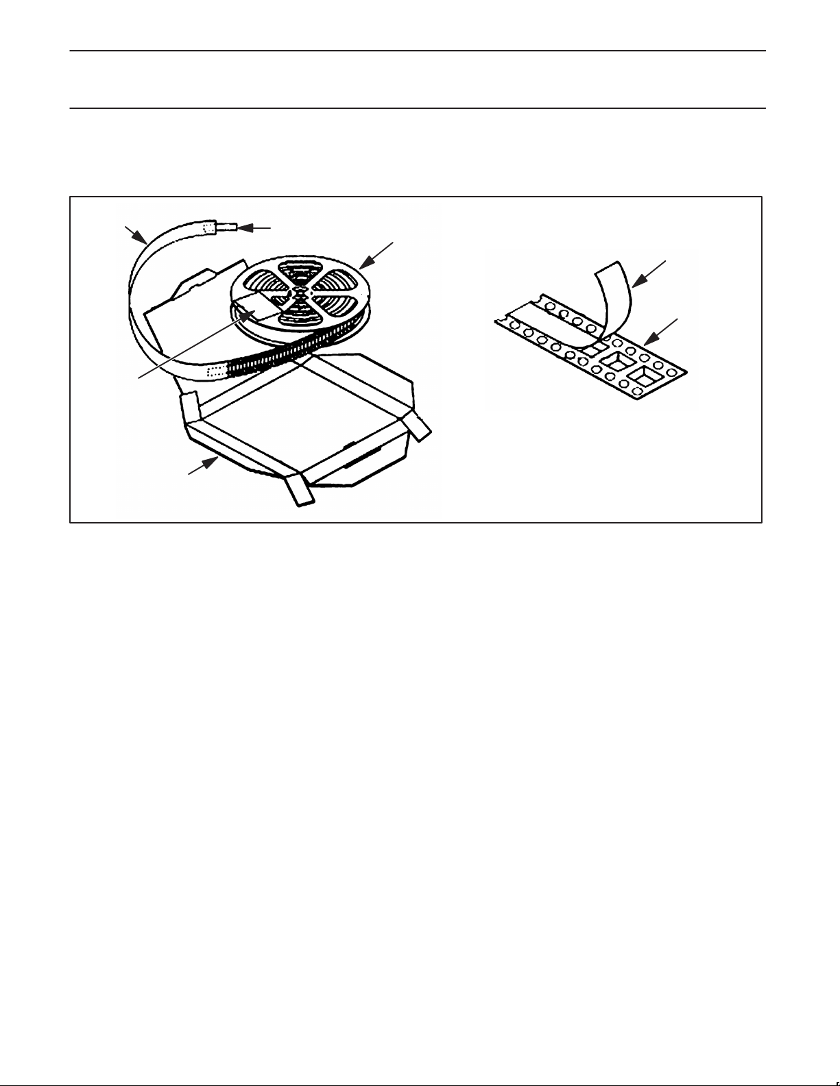
PACKING METHOD
The NE56604-42 is packed in reels, as shown in Figure 28.
GUARD
BAND
BARCODE
LABEL
BOX
TAPE
REEL
ASSEMBLY
Figure 28. Tape and reel packing method
TAPE DETAIL
COVER TAPE
CARRIER TAPE
SL01305
2001 Aug 22
15
Page 16

Philips Semiconductors Product data
NE56604-42System reset with built-in watchdog timer
SO8: plastic small outline package; 8 leads; body width 3.9 mm
1.73
0.068
pin 1 index
B
2
4.95
4.80
0.189
0.195
0.51
0.33
0.013
0.020
4.95
4.80
1.27
0.38
0.050
0.015
0.076
0.003
2001 Aug 22
SO8
16
Page 17

Philips Semiconductors Product data
NE56604-42System reset with built-in watchdog timer
NOTES
2001 Aug 22
17
Page 18

Philips Semiconductors Product data
NE56604-42System reset with built-in watchdog timer
Data sheet status
Product
Data sheet status
Objective data
Preliminary data
Product data
[1] Please consult the most recently issued data sheet before initiating or completing a design.
[2] The product status of the device(s) described in this data sheet may have changed since this data sheet was published. The latest information is available on the Internet at URL
http://www.semiconductors.philips.com.
[1]
status
Development
Qualification
Production
[2]
Definitions
Short-form specification — The data in a short-form specification is extracted from a full data sheet with the same type number and title. For
detailed information see the relevant data sheet or data handbook.
Limiting values definition — Limiting values given are in accordance with the Absolute Maximum Rating System (IEC 60134). Stress above one
or more of the limiting values may cause permanent damage to the device. These are stress ratings only and operation of the device at these or
at any other conditions above those given in the Characteristics sections of the specification is not implied. Exposure to limiting values for extended
periods may affect device reliability.
Application information — Applications that are described herein for any of these products are for illustrative purposes only. Philips
Semiconductors make no representation or warranty that such applications will be suitable for the specified use without further testing or
modification.
Disclaimers
Life support — These products are not designed for use in life support appliances, devices or systems where malfunction of these products can
reasonably be expected to result in personal injury . Philips Semiconductors customers using or selling these products for use in such applications
do so at their own risk and agree to fully indemnify Philips Semiconductors for any damages resulting from such application.
Right to make changes — Philips Semiconductors reserves the right to make changes, without notice, in the products, including circuits, standard
cells, and/or software, described or contained herein in order to improve design and/or performance. Philips Semiconductors assumes no
responsibility or liability for the use of any of these products, conveys no license or title under any patent, copyright, or mask work right to these
products, and makes no representations or warranties that these products are free from patent, copyright, or mask work right infringement, unless
otherwise specified.
Contact information
For additional information please visit
http://www.semiconductors.philips.com . Fax: +31 40 27 24825
For sales offices addresses send e-mail to:
sales.addresses@www.semiconductors.philips.com.
Definitions
This data sheet contains data from the objective specification for product development.
Philips Semiconductors reserves the right to change the specification in any manner without notice.
This data sheet contains data from the preliminary specification. Supplementary data will be
published at a later date. Philips Semiconductors reserves the right to change the specification
without notice, in order to improve the design and supply the best possible product.
This data sheet contains data from the product specification. Philips Semiconductors reserves the
right to make changes at any time in order to improve the design, manufacturing and supply.
Changes will be communicated according to the Customer Product/Process Change Notification
(CPCN) procedure SNW-SQ-650A.
Koninklijke Philips Electronics N.V. 2001
All rights reserved. Printed in U.S.A.
Date of release: 10-01
Document order number: 9397 750 08732
2001 Aug 22
18
 Loading...