

Page 1

INTEGRATED CIRCUITS
74F579
8-bit bidirectional binary counter (3-State)
Product specification
IC15 Data Handbook
1992 May 04
Page 2
Philips Semiconductors Product specification
I/O
74F5798-bit bidirectional binary counter (3-State)
FEA TURES
•Fully synchronous operation
•Multiplexed 3-State I/O ports for bus oriented applications
•Built in cascading carry capability
•U/D pin to control direction of counting
•Separate pins for Master reset and Synchronous operation
•Center power pins to reduce effects of package inductance
•Count frequency 115MHz Typ
•Supply current 100mA Typ
•See 74F269 for 24-pin separate I/O port version
•See 74F779 for 16-pin version
DESCRIPTION
The 74F579 is a fully synchronous 8-stage Up/Down Counter with
multiplexed 3-State I/O ports for bus-oriented applications. It
features a preset capability for programmable operation, carry
look-ahead for easy cascading and a U/D
direction of counting. All state changes, except for the case of
asynchronous reset, are initiated by the rising edge of the clock.
TC
output is not recommended for use as a clock or asynchronous
reset due to the possibility of decoding spikes.
input to control the
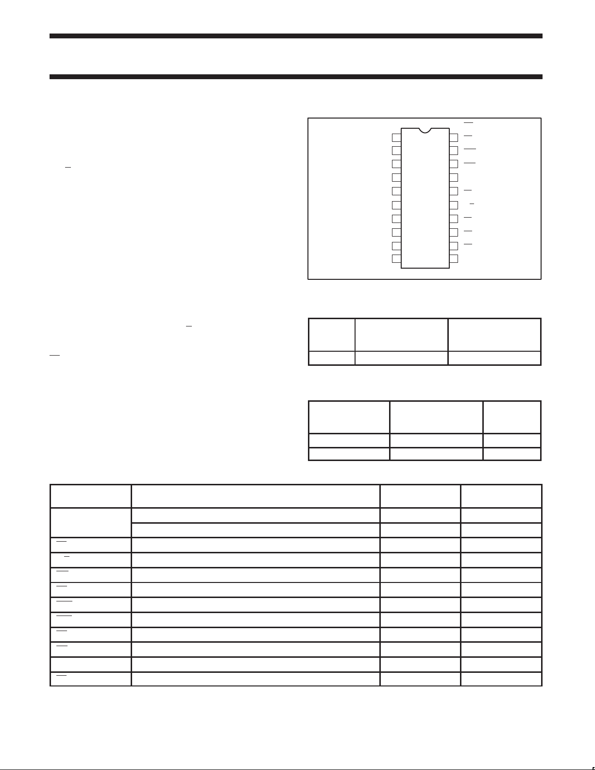
PIN CONFIGURATION
CP
1
I/O0
2
I/O1
3
I/O2
4
I/O3
5
GND
6
I/O4
7
I/O5
8
I/O6
9
I/O7
10 11
20
19
18
17
16
15
14
13
12
SF01085
MR
SR
CEP
CET
VCC
TC
U/D
PE
CS
OE
ORDERING INFORMA TION
TYPICAL SUPPL Y
TYPE TYPICAL f
MAX
74F579 115MHz 100mA
CURRENT
(TOTAL)
ORDERING INFORMATION
COMMERCIAL RANGE
DESCRIPTION
VCC = 5V ±10%,
T
= 0°C to +70°C
amb
PKG DWG #
20-Pin Plastic DIP N74F579N SOT146-1
20-Pin Plastic SOL N74F579D SOT163-1
INPUT AND OUTPUT LOADING AND FAN-OUT TABLE
PINS DESCRIPTION
74F(U.L.)
HIGH/LOW
Data Inputs 3.5/1.0 70µA/0.6mA
n
Data Outputs 150/40 3.0mA/24mA
PE Parallel Enable input (active Low) 1.0/1.0 20µA/0.6mA
U/D Up/Down count control input 1.0/1.0 20µA/0.6mA
MR Master Reset input (active Low) 1.0/1.0 20µA/0.6mA
SR Synchronous Reset input (active Low) 1.0/1.0 20µA/0.6mA
CEP Count Enable Parallel input (active Low) 1.0/1.0 20µA/0.6mA
CET Count Enable Trickle input (active Low) 1.0/1.0 20µA/0.6mA
CS Chip Select input (active Low) 1.0/1.0 20µA/0.6mA
OE Output Enable input (active Low) 1.0/1.0 20µA/0.6mA
CP Clock input (active Rising Edge) 1.0/1.0 20µA/0.6mA
TC Terminal Count Output (active Low) 50/33 1.0mA/20mA
NOTE: One (1.0) FAST Unit Load (U.L.) is defined as: 20µA in the High state and 0.6mA in the Low state.
LOAD VALUE
HIGH/LOW
1992 May 04 853-0377 06639
2
Page 3
Philips Semiconductors Product specification
74F5798-bit bidirectional binary counter (3-State)
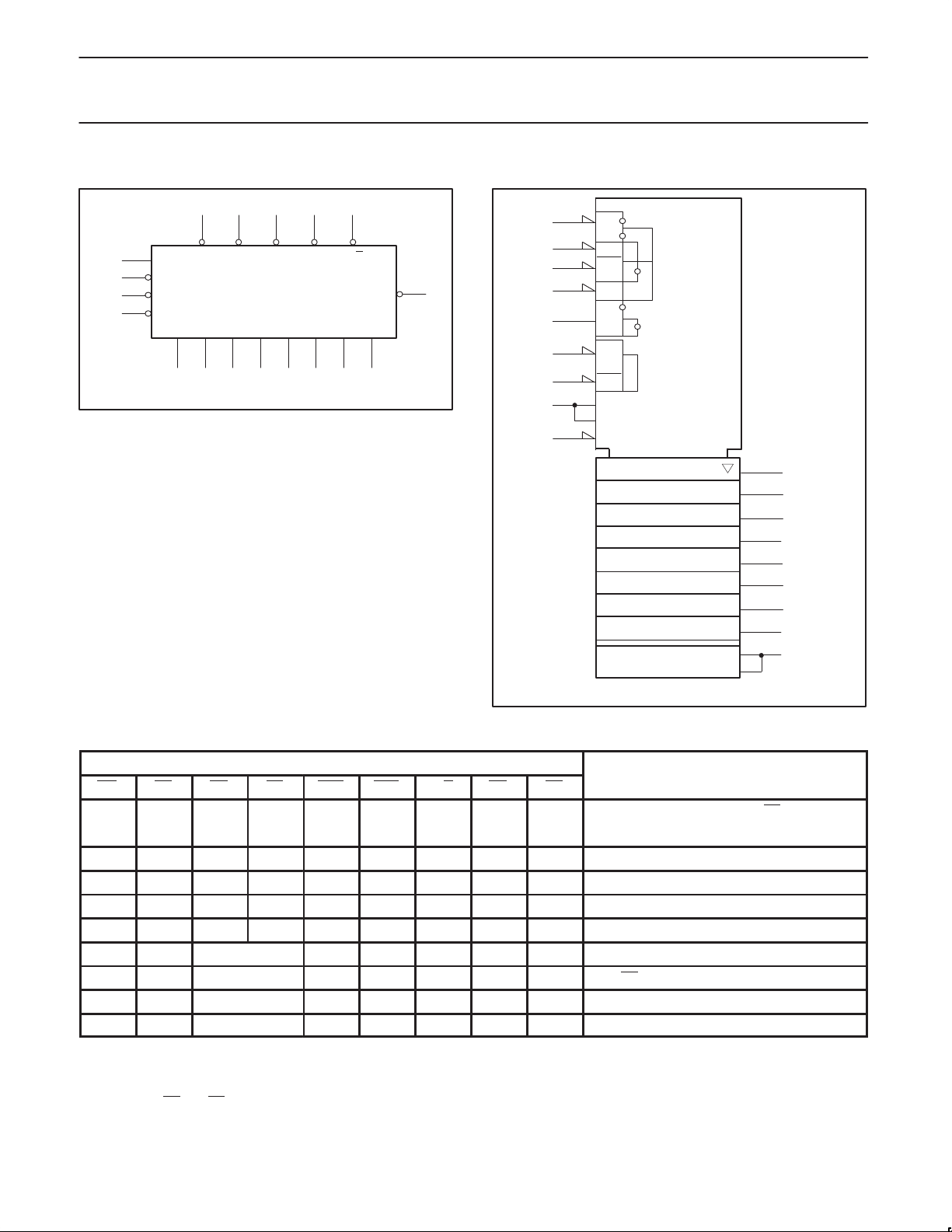
LOGIC SYMBOL
1
CP
18
17
11
= Pin 16
V
CC
GND = Pin 6
CEP
CET
OE
I/O0 I/O1 I/O4 I/O5 I/O6 I/O7
2
13
12 20 19 14
PE
CS MR SR U/D
I/O2 I/O3
34578910
TC
SF01086
LOGIC SYMBOL (IEEE/IEC)
19
12
13
11
15
14
17
18
1
20
R1
1
1
1
&
1
1
1
M4[DOWN]
1
EN6
1
&
1
2,5,7, +/C8
2,4,7–
R9
CTR DIV 256
M2[LOAD]
&
EN3
M5[UP]
G7
[1]
[2]
[4]
[8]
[16]
[32]
[64]
[128]
3,5,6,8 CT=256
3,4,6,8 CT=0
1,2,3,4,
5,6,7,8
2
3
4
5
6
8
9
10
15
SF01087
FUNCTION TABLE
INPUTS OPERATING MODE
MR SR CS PE CEP CET U/D OE CP
X X H X X X X X X I/O0 to I/O7 in high impedance (PE disabled)
X X L H X X X H X I/O0 to I/O7 in high impedance
X X L H X X X L X Flip-flop output appears on I/On lines
L X X X X X X X X Asynchronous reset for all flip-flops
H L X X X X X X ↑ Synchronous reset for all flip-flops
H H L L X X X X ↑ Parallel load all flip-flops
H H (not LL) H X X X ↑ Hold
H H (not LL) X H X X ↑ Hold (TC held High)
H H (not LL) L L H X ↑ Count up
H H (not LL) L L L X ↑ Count down
H = High voltage level
L = Low voltage level
X = Don’t care
↑ = Low-to-High clock transition
(not LL) = CS
and PE should never be Low voltage level at the same time.
1992 May 04
3
Page 4
Philips Semiconductors Product specification
74F5798-bit bidirectional binary counter (3-State)
LOGIC DIAGRAM
19
SR
13
OE
PE
CS
12
11
CP
MR
1
20
I/O0
I/O1
I/O2
I/O3
I/O4
I/O5
2
3
4
5
7
8
DETAIL A
DETAIL A
DETAIL A
DETAIL A
DETAIL A
DETAIL A
VCC=pin 16
GND=pin 6
1992 May 04
U/D
CEP
CET
TC
9
I/O6
10
I/O7
14
18
17
DATA
LOAD
15
Q
Q
For pinouts refer to Package Pin Configurations
DETAIL A
DETAIL A
TOGGLE
DETAIL A
CP
MR
Q
D
Q
CP
SF01088
4
Page 5
Philips Semiconductors Product specification
IOCurrent applied to output in Low output state
IOHHigh-level output current
IOLLow-level output current
74F5798-bit bidirectional binary counter (3-State)
ABSOLUTE MAXIMUM RATINGS
(Operation beyond the limits set forth in this table may impair the useful life of the device.
Unless otherwise noted these limits are over the operating free-air temperature range.)
SYMBOL
V
V
I
V
T
T
CC
IN
IN
O
amb
stg
Supply voltage –0.5 to +7.0 V
Input voltage –0.5 to +7.0 V
Input current –30 to +5 mA
Voltage applied to output in High output state –0.5 to +V
pp
p
Operating free-air temperature range 0 to +70 °C
Storage temperature –65 to +150 °C
RECOMMENDED OPERATING CONDITIONS
SYMBOL PARAMETER LIMITS UNIT
V
V
V
I
T
CC
IH
IL
IK
amb
Supply voltage 4.5 5.0 5.5 V
High-level input voltage 2.0 V
Low-level input voltage 0.8 V
Input clamp current –18 mA
p
p
Operating free-air temperature range 0 70 °C
PARAMETER RATING UNIT
CC
p
TC 40 mA
I/O0 48 mA
MIN NOM MAX
TC –1 mA
I/O
n
–3 mA
TC 20 mA
I/O
n
24 mA
V
1992 May 04
5
Page 6

Philips Semiconductors Product specification
SYMBOL
PARAMETER
TEST CONDITIONS
1
UNIT
TC
V
MAX
I
1mA
VOHHigh-level output voltage
IH
I/O
V
I
3mA
VOLLow-level output voltage
V
MAX
I
MAX
I
I/O
74F5798-bit bidirectional binary counter (3-State)
DC ELECTRICAL CHARACTERISTICS
(Over recommended operating free-air temperature range unless otherwise noted.)
LIMITS
MIN TYP
V
I
I
IH
I
IL
I
OZH
I
OZL
I
OS
I
CC
VCC = MIN,
=
IL
p
n
V
(VIL = 0.0V,
IH
for MR, CP inputs)
,
= MIN
= 4.5V
OH
OH
= –
= –
VCC = MIN,
p
IK
+ I
Input clamp voltage VCC = MIN, II = I
I/O
Input current
at maximum input voltage
High-level input current
Low-level input current
Off-state output current
+ I
IH
High-level voltage applied
Off-state output current
IL
Low-level voltage applied
Short-circuit output current
Supply current (total) I
3
n
others VCC = MAX, VI = 7.0V 100
except
I/O
n
n
I
CCH
CCL
I
CCZ
=
IL
VIH = MIN
VCC = MAX, VI = 5.5V 1 mA
VCC = MAX, VI = 2.7V 20
VCC = MAX, VI = 0.5V –0.6 mA
VCC = MAX, VO = 2.7V 70
VCC = MAX, VO = 0.5V –600
OL
=
,
VCC = MAX –60 –150 mA
VCC = MAX 105 145 mA
±10%V
±5%V
CC
±10%V
±5%V
CC
±10%V
,
±5%V
CC
IK
2.5 V
CC
2.7 3.4 V
2.4 3.3 V
CC
2.7 3.3 V
CC
NOTES:
1. For conditions shown as MIN or MAX, use the appropriate value specified under Recommended Operating Conditions for the applicable
type.
2. All typical values are at V
3. Not more than one output should be shorted at a time. For testing I
= 5V, T
CC
techniques are preferable in order to minimize internal heating and more accurately reflect operational values. Otherwise, prolonged shorting
amb
= 25°C.
, the use of high-speed test apparatus and/or sample-and-hold
OS
of a High output may raise the chip temperature well above normal and thereby cause invalid readings in other parameter tests. In any
sequence of parameter test, I
tests should be performed last.
OS
2
MAX
0.35 0.50 V
0.35 0.50 V
–0.73 –1.2 V
95 135 mA
105 150 mA
µA
µA
µA
µA
1992 May 04
6
Page 7

Philips Semiconductors Product specification
74F5798-bit bidirectional binary counter (3-State)
AC ELECTRICAL CHARACTERISTICS
LIMITS
T
SYMBOL PARAMETER TEST CONDITIONS
f
MAX
t
PLH
t
PHL
t
PLH
t
PHL
t
PLH
t
PHL
t
PLH
t
PHL
t
PHL
t
PLH
t
PHL
t
PZH
t
PZL
t
PHZ
t
PLZ
t
PZH
t
PZL
t
PHZ
t
PLZ
t
PZH
t
PZL
t
PHZ
t
PLZ
Maximum clock frequency Waveform 1 100 115 80 MHz
Propagation delay
CP to I/O
n
Propagation delay
CP to TC
Propagation delay
U/D to TC
Propagation delay
CET to TC
Propagation delay
MR to I/O
n
Propagation delay
MR to TC
Output Enable time
CS to I/O
n
Output Disable time
CS to I/O
n
Output Enable time
PE to I/O
n
Output Disable time
PE to I/O
n
Output Disable time
OE to I/O
n
Output Enable time
OE
to I/O
n
Waveform 1
Waveform 1
Waveform 4
Waveform 3
Waveform 2 5.0 7.0 9.0 5.0 10.0 ns
Waveform 4
Waveform 6
Waveform 7
Waveform 6
Waveform 7
Waveform 6
Waveform 7
Waveform 6
Waveform 7
Waveform 6
Waveform 7
Waveform 6
Waveform 7
= +25°C
amb
VCC = +5.0V
CL = 50pF, RL = 500Ω
MIN TYP MAX MIN MAX
5.0
5.0
5.5
5.5
3.5
4.5
3.5
3.5
4.0
6.0
4.0
5.5
3.0
5.0
3.0
5.0
3.0
2.5
2.5
4.5
1.0
2.0
7.5
7.5
7.5
7.5
5.5
6.5
5.5
6.0
6.5
8.0
5.0
7.0
5.0
7.5
4.5
6.5
4.0
4.0
4.0
5.5
2.5
4.0
10.5
10.5
10.0
10.0
8.0
8.0
7.0
8.0
9.0
10.5
8.5
10.5
7.5
9.5
8.0
10.0
7.5
7.5
7.0
9.0
4.0
7.0
T
= 0°C to +70°C
amb
VCC = +5.0V ± 10%
CL = 50pF, RL = 500Ω
4.5
5.0
5.0
5.0
3.5
4.5
3.5
3.5
4.0
6.0
3.5
5.0
3.0
4.5
3.0
4.5
3.0
2.0
2.5
4.0
1.0
2.0
11.5
11.5
11.0
11.0
9.0
9.0
8.5
8.5
10.5
12.5
10.0
11.5
9.0
11.0
9.0
11.0
9.0
8.5
8.5
10.5
5.5
8.0
UNIT
ns
ns
ns
ns
ns
ns
ns
ns
ns
ns
ns
ns
ns
ns
ns
ns
ns
ns
ns
ns
ns
ns
1992 May 04
7
Page 8

Philips Semiconductors Product specification
74F5798-bit bidirectional binary counter (3-State)
AC SETUP REQUIREMENTS
LIMITS
T
= +25°C
amb
SYMBOL PARAMETER TEST CONDITIONS
ts(H)
ts(L)
th(H)
th(L)
ts(H)
ts(L)
th(H)
th(L)
ts(H)
ts(L)
th(H)
th(L)
ts(H)
ts(L)
th(H)
th(L)
tw(H)
tw(L)
tw(L) MR Pulse width, Low Waveform 2 3.0 3.0 ns
t
rec
Setup time, High or Low
I/On to CP
Hold time, High or Low
I/On to CP
Setup time, High or Low
U/D to CP
Hold time, High or Low
U/D to CP
Setup time, High or Low
PE, SR or CS to CP
Hold time, High or Low
PE, SR or CS to CP
Setup time, High or Low
CEP or CET to CP
Hold time, High or Low
CEP or CET to CP
CP Pulse width, High or Low Waveform 1
Recovery time, MR to CP Waveform 2 4.0 4.5 ns
Waveform 5
Waveform 5
Waveform 5
Waveform 5
Waveform 5
Waveform 5
Waveform 5
Waveform 5
VCC = +5.0V
CL = 50pF, RL = 500Ω
MIN TYP MAX MIN MAX
3.0
3.0
0
0
8.0
8.0
0
0
9.5
9.5
0
0
5.0
9.0
0
0
4.5
4.5
T
= 0°C to +70°C
amb
VCC = +5.0V ± 10%
CL = 50pF, RL = 500Ω
4.0
4.0
0
0
9.0
9.0
0
0
10.0
10.0
0
0
5.5
10.5
0
0
4.5
4.5
UNIT
ns
ns
ns
ns
ns
ns
ns
ns
ns
ns
ns
ns
ns
ns
ns
ns
ns
ns
1992 May 04
8
Page 9

Philips Semiconductors Product specification
74F5798-bit bidirectional binary counter (3-State)
AC WAVEFORMS
NOTE: For all waveforms VM = 1.5V.
The shaded areas indicate when the input is permitted to change for predictable output performance.
1/f
I/O
CP
TC
MAX
MR
V
M
tW(H) tW(L)
t
PLH
V
n
M
t
PHL
V
M
V
t
t
PHL
PLH
M
CP
V
M
I/O
n
V
M
V
M
tW(L) t
t
PHL
V
M
V
M
rec
V
M
SF01089
Waveform 1. Propagation Delay, Clock Input to Output,
Clock Pulse Width and Maximum Clock Frequency
CET
V
M
t
PHL
TC
V
V
M
t
PLH
M
V
M
SF01091
Waveform 3. Propagation Delay, CET Input to
Terminal Count Output
PE
, CS,
, SR,
U/D
I/On, CEP,
CET
CP
V
V
M
M
ts(H) ts(L)
t
(L) th(L)
h
V
M
VMV
Waveform 5. Setup and Hold Times
M
V
M
SF01093
SF01090
Waveform 2. Master Reset Pulse Width, Master Reset to
Output Delay and Master Reset to Clock Recovery Time
MR, U/D
TC
V
M
t
PHL
V
M
V
M
t
PLH
SF01092
Waveform 4. Propagation Delay, U/D and MR Inputs to
Terminal Count Output
PE, OE,
I/O
CS
V
M
t
PZH
n
V
V
M
t
PHZ
M
VOH -0.3V
SF01094
Waveform 6. 3-State Output Enable Time to High Level and
Output Disable Time from High Level
, OE,
PE
I/O
CS
n
V
M
t
PZL
V
V
M
t
PLZ
M
VOL +0.3V
SF01095
Waveform 7. 3-State Output Enable Time to Low Level and
Output Disable Time from Low Level
1992 May 04
9
Page 10

Philips Semiconductors Product specification
74F5798-bit bidirectional binary counter (3-State)
TEST CIRCUIT AND WAVEFORMS
V
V
PULSE
GENERATOR
IN
R
Test Circuit for 3-State Outputs
SWITCH POSITION
TEST SWITCH
t
t
PLZ
PZL
closed
closed
All other open
T
D.U.T.
CC
V
OUT
7.0V
R
L
C
R
L
L
NEGATIVE
PULSE
POSITIVE
PULSE
90%
10%
V
M
10%
t
THL (tf
t
TLH (tr
90%
V
M
Input Pulse Definition
t
w
V
M
10%
)
)
t
)
TLH (tr
t
)
THL (tf
90%
V
M
t
w
90%
10%
AMP (V)
0V
AMP (V)
0V
DEFINITIONS:
= Load resistor;
R
L
see AC electrical characteristics for value.
C
= Load capacitance includes jig and probe capacitance;
L
see AC electrical characteristics for value.
R
= Termination resistance should be equal to Z
T
pulse generators.
OUT
of
family
74F
INPUT PULSE REQUIREMENTS
V
amplitude
3.0V
M
1.5V
rep. rate
1MHz 500ns
t
w
t
TLHtTHL
2.5ns 2.5ns
SF00777
1992 May 04
10
Page 11

Philips Semiconductors Product specification
8-bit bidirectional binary counter (3-State)
DIP20: plastic dual in-line package; 20 leads (300 mil) SOT146-1
74F579
1992 May 04
11
Page 12

Philips Semiconductors Product specification
8-bit bidirectional binary counter (3-State)
SO20: plastic small outline package; 20 leads; body width 7.5 mm SOT163-1
74F579
1992 May 04
12
Page 13

Philips Semiconductors Product specification
8-bit bidirectional binary counter (3-State)
NOTES
74F579
1992 May 04
13
Page 14

Philips Semiconductors Product specification
8-bit bidirectional binary counter (3-State)
Data sheet status
Data sheet
status
Objective
specification
Preliminary
specification
Product
specification
Product
status
Development
Qualification
Production
Definition
This data sheet contains the design target or goal specifications for product development.
Specification may change in any manner without notice.
This data sheet contains preliminary data, and supplementary data will be published at a later date.
Philips Semiconductors reserves the right to make chages at any time without notice in order to
improve design and supply the best possible product.
This data sheet contains final specifications. Philips Semiconductors reserves the right to make
changes at any time without notice in order to improve design and supply the best possible product.
[1]
74F579
[1] Please consult the most recently issued datasheet before initiating or completing a design.
Definitions
Short-form specification — The data in a short-form specification is extracted from a full data sheet with the same type number and title. For
detailed information see the relevant data sheet or data handbook.
Limiting values definition — Limiting values given are in accordance with the Absolute Maximum Rating System (IEC 134). Stress above one
or more of the limiting values may cause permanent damage to the device. These are stress ratings only and operation of the device at these or
at any other conditions above those given in the Characteristics sections of the specification is not implied. Exposure to limiting values for extended
periods may affect device reliability.
Application information — Applications that are described herein for any of these products are for illustrative purposes only. Philips
Semiconductors make no representation or warranty that such applications will be suitable for the specified use without further testing or
modification.
Disclaimers
Life support — These products are not designed for use in life support appliances, devices or systems where malfunction of these products can
reasonably be expected to result in personal injury . Philips Semiconductors customers using or selling these products for use in such applications
do so at their own risk and agree to fully indemnify Philips Semiconductors for any damages resulting from such application.
Right to make changes — Philips Semiconductors reserves the right to make changes, without notice, in the products, including circuits, standard
cells, and/or software, described or contained herein in order to improve design and/or performance. Philips Semiconductors assumes no
responsibility or liability for the use of any of these products, conveys no license or title under any patent, copyright, or mask work right to these
products, and makes no representations or warranties that these products are free from patent, copyright, or mask work right infringement, unless
otherwise specified.
Philips Semiconductors
811 East Arques Avenue
P.O. Box 3409
Sunnyvale, California 94088–3409
Telephone 800-234-7381
Copyright Philips Electronics North America Corporation 1998
All rights reserved. Printed in U.S.A.
print code Date of release: 10-98
Document order number: 9397-750-05142
yyyy mmm dd
14
 Loading...