

Page 1

INTEGRATED CIRCUITS
74F283
4-bit binary full adder with fast carry
Product specification
IC15 Data Handbook
1989 Mar 03
Page 2
Philips Semiconductors Product specification
74F2834-bit binary full adder with fast carry
FEA TURES
•High speed 4-bit addition
•Cascadable in 4-bit increments
•Fast Internal carry look-ahead
DESCRIPTION
The 74F283 adds two 4-bit binary words (An plus Bn) plus the
incoming carry. The binary sum appears on the sum outputs
(Σ0–Σ3) and the outgoing carry (C
C
+20(A0+B0)+21(A1+B1)+22(A2+B2)+23(A3+B3)
IN
=Σ0+2Σ1+4Σ2+8Σ3+16C
OUT
where (+)=plus
Due to the symmetry of the binary add function, the 74F283 can be
used with either all active-High operands (positive logic) or with all
active-Low operands (negative logic). See Function Table. In case of
all active-Low operands (negative logic) the results Σ1–Σ4 and C
should be interpreted also as active-Low. With active-High inputs,
C
cannot be left open; it must be held Low when no “carry in” is
IN
intended. Interchanging inputs of equal weight does not affect the
operation, thus A0, B0, C
can arbitrarily be assigned to pins 5, 6,
IN
7, etc.
Due to pin limitations, the intermediate carries of the 74F283 are not
brought out for use as inputs or outputs. However, other means can
be used to effectively insert a carry into, or bring a carry out from, an
intermediate stage.
) according to the equation:
OUT
OUT
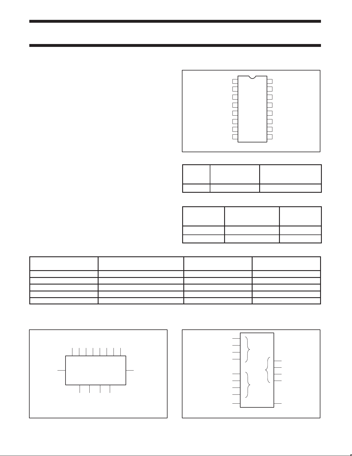
PIN CONFIGURATION
1
Σ1
2
B1
3
A1
Σ0
4
5
A0
6
B0
7
C
IN
8
GND
TYPICAL
TYPE
PROPAGATION
DELAY
74F283 6.5ns 40mA
V
16
CC
15
B2
14
A2
Σ2
13
12
A3
11
B3
10
Σ3
C
9
OUT
SF00852
TYPICAL
SUPPLY CURRENT
(TOTAL)
ORDERING INFORMATION
COMMERCIAL RANGE
DESCRIPTION
16-pin plastic DIP N74F283N SOT38-4
16-pin plastic SO N74F283D SOT109-1
VCC = 5V ±10%,
T
= 0°C to +70°C
amb
PKG DWG #
INPUT AND OUTPUT LOADING AND FAN-OUT TABLE
PINS DESCRIPTION
A0 - A3 A operand inputs 1.0/2.0 20µA/1.2mA
B0 - B3 B operand inputs 1.0/2.0 20µA/1.2mA
C
C
OUT
IN
Carry input 1.0/1.0 20µA/0.6mA
Carry output 50/33 1.0mA/20mA
Σ0–Σ3 Sum outputs 50/33 1.0mA/20mA
NOTE:
One (1.0) FAST Unit Load is defined as: 20µA in the High state and 0.6mA in the Low state.
LOGIC SYMBOL
C
VCC=Pin 16
GND=Pin 8
5 6 3 2 14 15 12 11
A0 B0 A1 B1 A2 B2 A3 B3
13 10
C
OUT
Σ3Σ2
IN
Σ1Σ0
41
97
SF00853
LOGIC SYMBOL (IEEE/IEC)
74F(U.L.)
HIGH/LOW
LOAD VALUE
HIGH/LOW
5
3
14
12
6
2
15
11
7
Σ
0
P
3
0
Q
3
0
4
3
SF00854
1
13
10
9
Σ
COCI
1989 Mar 03 853-0364 95944
2
Page 3
Philips Semiconductors Product specification
1001
(10+9=19)
74F2834-bit binary full adder with fast carry
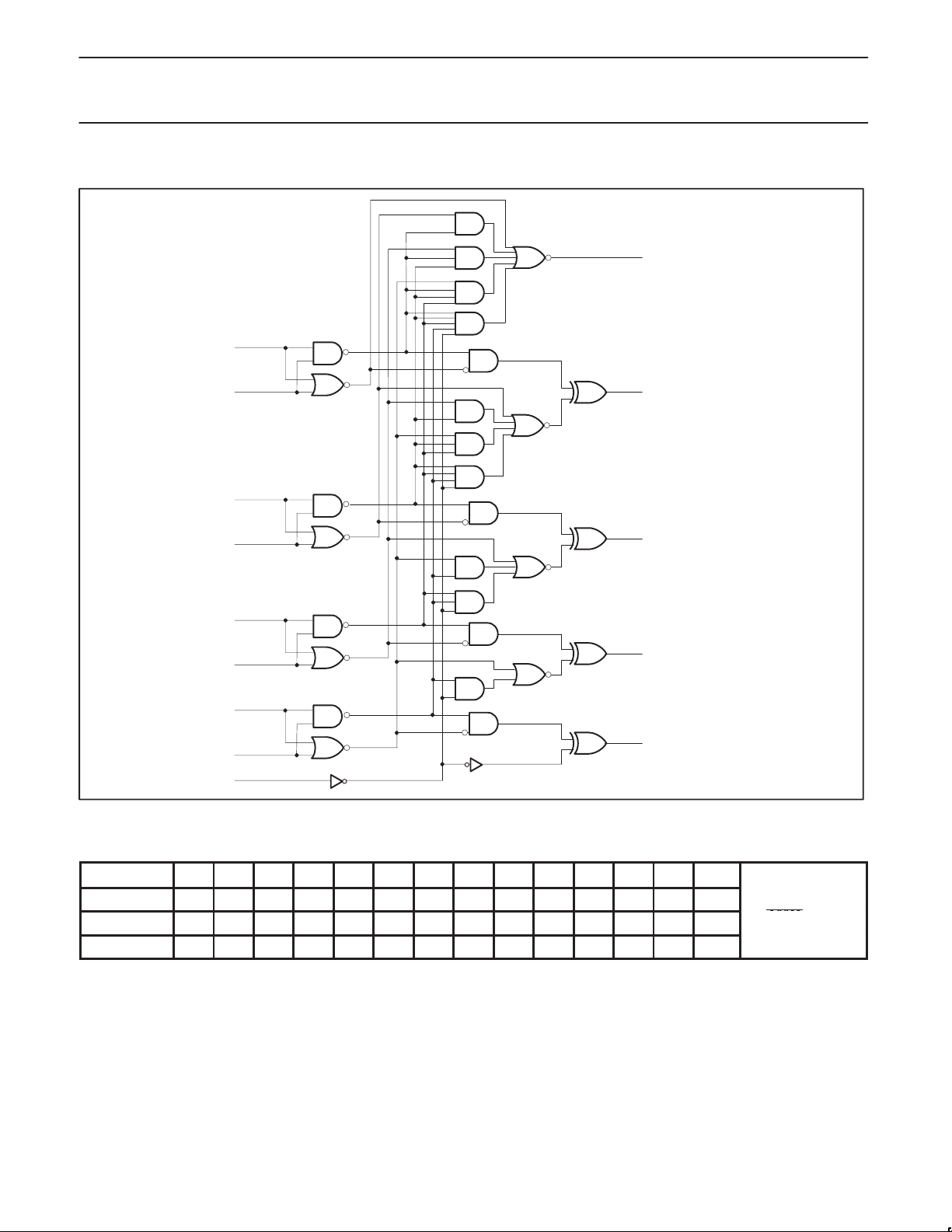
LOGIC DIAGRAM
9
C
OUT
11
B3
=Pin 16
V
CC
GND=Pin 8
12
A3
15
B2
14
A2
2
B1
3
A1
6
B0
5
A0
7
C
IN
10
13
1
4
SF00855
Σ3
Σ2
Σ1
Σ0
FUNCTION TABLE
PINS C
Logic levels L L H L H H L L H H H L L H
Active High 0 0 1 0 1 1 0 0 1 1 1 0 0 1
Active Low 1 1 0 1 0 0 1 1 0 0 0 1 1 0
H = High voltage level
L = Low voltage level
1989 Mar 03
A0 A1 A2 A3 B0 B1 B2 B3 Σ0 Σ1 Σ2 Σ3 C
IN
3
OUT
Example:
1010
10011
(carry+5+6=12)
Page 4

Philips Semiconductors Product specification
74F2834-bit binary full adder with fast carry
Figure A shows how to make a 3-bit adder. Tying the operand inputs
of the fourth adder (A3, B3) Low makes Σ3 dependent only on, and
equal to, the carry from the third adder. Using somewhat the same
principle, Figure B shows a way of dividing the 74F283 into a 2-bit
and a 1-bit adder. The third stage adder (A2, B2, Σ2) is used as
means of getting a carry (C10) signal into the fourth stage adder (via
A2 and B2) and bringing out the carry from the second stage on Σ2.
Note that as long as A2 and B2 are the same, whether High or Low,
APPLICATIONS
L
A0 B0 A1 B1 A2 B2 A3 B3
C
IN
Σ1Σ0
A. 3-bit Adder
I0 I1
A0 B0 A1 B1 A2 B2 A3 B3
C
OUT
Σ3Σ2
C3
I2
I3 I4L
they do not influence Σ2. Similarly , when A2 and B2 are the same,
the carry into the third stage does not influence the carry out of the
third stage. Figure C shows a method of implementing a 5-input
encoder where the inputs are equally weighted. The outputs Σ0, Σ1
and Σ2 present a binary number of inputs I0–I4 that are true.
Figure D shows one method of implementing a 5-input majority gate.
When three or more of the inputs I0–I4 are true, the output M4 is
true.
C10
A0 B0 A1 B1
A0 B0 A1 B1 A2 B2 A3 B3
C
C
IN
IN
Σ1Σ0
Σ1Σ0 Σ10C2
A10 B10
C
Σ3Σ2
OUT
C
11
B. 2-bit and 1-bit Adder
I0 I1
A0 B0 A1 B1 A2 B2 A3 B3
I2
I3 I4
C
IN
Σ1Σ0
20212
2
C. 5-input Encoder
C
OUT
Σ3Σ2
C
IN
Σ1Σ0
C
Σ3Σ2
M4
D. 5-input Majority Gate
OUT
SF00856
1989 Mar 03
4
Page 5

Philips Semiconductors Product specification
SYMBOL
PARAMETER
UNIT
NO TAG
VOHHigh-level output voltage
V
VOLLow-level output voltage
V
IILLow-level input current
V
MAX, V
5V
74F2834-bit binary full adder with fast carry
ABSOLUTE MAXIMUM RATINGS
(Operation beyond the limits set forth in this table may impair the useful life of the device. Unless otherwise noted these limits are over the
operating free-air temperature range.)
SYMBOL PARAMETER RATING UNIT
V
CC
V
IN
I
IN
V
OUT
I
OUT
T
amb
T
stg
RECOMMENDED OPERATING CONDITIONS
V
CC
V
IH
V
IL
I
IK
I
OH
I
OL
T
amb
Supply voltage –0.5 to +7.0 V
Input voltage –0.5 to +7.0 V
Input current –30 to +5 mA
Voltage applied to output in High output state –0.5 to V
CC
V
Current applied to output in Low output state 40 mA
Operating free-air temperature range 0 to +70 °C
Storage temperature –65 to +150 °C
LIMITS
Min Nom Max
Supply voltage 4.5 5.0 5.5 V
High-level input voltage 2.0 V
Low-level input voltage 0.8 V
Input clamp current –18 mA
High-level output current –1
mA
Low-level output current 20 mA
Operating free-air temperature range 0 70 °C
DC ELECTRICAL CHARACTERISTICS
(Over recommended operating free-air temperature range unless otherwise noted.)
LIMITS
SYMBOL PARAMETER TEST CONDITIONS
p
p
V
IK
I
I
I
IH
I
OS
I
CC
Input clamp voltage VCC = MIN, II = I
Input current at maximum input voltage VCC = MAX, VI = 7.0V 100 µA
High-level input current VCC = MAX, VI = 2.7V 20 µA
p
Short-circuit output current
Supply current (total)
CIN only
An, Bn
NO TAG
4
VCC = MIN, VIL = MAX ±10%V
VIH = MIN, IOH = MAX ±5%V
VCC = MIN, VIL = MAX ±10%V
VIH = MIN, IOL = MAX ±5%V
IK
CC
=
= 0.
I
VCC = MAX –60 –150 mA
VCC = MAX 40 55 mA
CC
CC
CC
CC
MIN
2.5
2.7 3.4
TYP
NO TAG
MAX
0.30 0.50
0.30 0.50
–0.73 –1.2 V
–0.6 mA
–1.2 mA
NOTES:
1. For conditions shown as MIN or MAX, use the appropriate value specified under recommended operating conditions for the applicable type.
2. All typical values are at V
3. Not more than one output should be shorted at a time. For testing I
= 5V, T
CC
techniques are preferable in order to minimize internal heating and more accurately reflect operational values. Otherwise, prolonged shorting
amb
= 25°C.
, the use of high-speed test apparatus and/or sample-and-hold
OS
of a High output may raise the chip temperature well above normal and thereby cause invalid readings in other parameter tests. In any
sequence of parameter tests, I
4. I
should be measured with all outputs open and the following conditions:
CC
Condition1: all inputs grounded
tests should be performed last.
OS
Condition 2: all B inputs Low, other inputs at 4.5V
Condition 3: all inputs at 4.5V
UNIT
1989 Mar 03
5
Page 6

Philips Semiconductors Product specification
TEST
V
V
V
10%
,
CONDITIONS
C
L
50pF,
C
L
50pF,
74F2834-bit binary full adder with fast carry
AC ELECTRICAL CHARACTERISTICS
LIMITS
T
SYMBOL PARAMETER
t
PLH
t
PHL
t
PLH
t
PHL
t
PLH
t
PHL
t
PLH
t
PHL
Propagation delay
CIN to Σi
Propagation delay
Ai or Bi to Σi
Propagation delay
C
to C
IN
OUT
Propagation delay
Ai or Bi to C
AC WAVEFORMS
For all waveforms, VM=1.5V.
OUT
Waveform 1, 2
Waveform 1, 2
Waveform 2
Waveform 1, 2
= +25°C
amb
= +5.
CC
C
= 50pF,
=
RL = 500Ω
MIN TYP MAX MIN MAX
3.5
4.0
3.5
3.5
3.5
3.0
3.5
2.5
7.0
7.0
7.0
7.0
5.7
5.4
5.7
5.3
9.5
9.5
9.5
9.5
7.5
7.0
7.5
7.0
T
= 0°C to +70°C
amb
= +5.V ±
CC
C
= 50pF
=
RL = 500Ω
3.0
3.5
2.5
3.5
3.5
2.5
3.0
2.5
10.5
10.5
10.5
10.5
8.5
8.0
8.5
8.0
UNIT
ns
ns
ns
ns
ns
ns
ns
ns
Ai, Bi, C
Σi, C
OUT
V
IN
M
t
PLH
V
M
V
M
Waveform 1. Propagation Delay
Operands and Carry Inputs to Outputs
TEST CIRCUIT AND WAVEFORM
V
CC
V
PULSE
GENERATOR
IN
R
T
Test Circuit for Totem-Pole Outputs
DEFINITIONS:
R
= Load resistor;
L
see AC ELECTRICAL CHARACTERISTICS for value.
= Load capacitance includes jig and probe capacitance;
C
L
see AC ELECTRICAL CHARACTERISTICS for value.
R
= Termination resistance should be equal to Z
T
pulse generators.
D.U.T.
V
OUT
C
Ai, Bi, C
t
PHL
IN
Σi, C
V
M
SF00857
OUT
V
M
t
PHL
V
M
V
M
t
PLH
V
M
SF00858
Waveform 2. Propagation Delay
Operands and Carry Inputs to Outputs
t
NEGATIVE
PULSE
R
L
L
POSITIVE
PULSE
90%
10%
V
M
10%
t
THL (tf
t
TLH (tr
90%
V
M
w
V
M
10%
)
)
t
w
t
TLH (tr
t
THL (tf
)
)
90%
V
M
90%
10%
AMP (V)
0V
AMP (V)
0V
Input Pulse Definition
INPUT PULSE REQUIREMENTS
V
amplitude
3.0V 1.5V
rep. rate
M
1MHz 500ns
t
w
t
TLHtTHL
2.5ns 2.5ns
OUT
of
family
74F
1989 Mar 03
SF00006
6
Page 7

Philips Semiconductors Product specification
4-bit binary full adder with fast carry
DIP16: plastic dual in-line package; 16 leads (300 mil) SOT38-4
74F283
1989 Mar 03
7
Page 8

Philips Semiconductors Product specification
4-bit binary full adder with fast carry
SO16: plastic small outline package; 16 leads; body width 3.9 mm SOT109-1
74F283
1989 Mar 03
8
Page 9

Philips Semiconductors Product specification
4-bit binary full adder with fast carry
74F283
NOTES
1989 Mar 03
9
Page 10

Philips Semiconductors Product specification
4-bit binary full adder with fast carry
Data sheet status
Data sheet
status
Objective
specification
Preliminary
specification
Product
specification
Product
status
Development
Qualification
Production
Definition
This data sheet contains the design target or goal specifications for product development.
Specification may change in any manner without notice.
This data sheet contains preliminary data, and supplementary data will be published at a later date.
Philips Semiconductors reserves the right to make chages at any time without notice in order to
improve design and supply the best possible product.
This data sheet contains final specifications. Philips Semiconductors reserves the right to make
changes at any time without notice in order to improve design and supply the best possible product.
[1]
74F283
[1] Please consult the most recently issued datasheet before initiating or completing a design.
Definitions
Short-form specification — The data in a short-form specification is extracted from a full data sheet with the same type number and title. For
detailed information see the relevant data sheet or data handbook.
Limiting values definition — Limiting values given are in accordance with the Absolute Maximum Rating System (IEC 134). Stress above one
or more of the limiting values may cause permanent damage to the device. These are stress ratings only and operation of the device at these or
at any other conditions above those given in the Characteristics sections of the specification is not implied. Exposure to limiting values for extended
periods may affect device reliability.
Application information — Applications that are described herein for any of these products are for illustrative purposes only. Philips
Semiconductors make no representation or warranty that such applications will be suitable for the specified use without further testing or
modification.
Disclaimers
Life support — These products are not designed for use in life support appliances, devices or systems where malfunction of these products can
reasonably be expected to result in personal injury . Philips Semiconductors customers using or selling these products for use in such applications
do so at their own risk and agree to fully indemnify Philips Semiconductors for any damages resulting from such application.
Right to make changes — Philips Semiconductors reserves the right to make changes, without notice, in the products, including circuits, standard
cells, and/or software, described or contained herein in order to improve design and/or performance. Philips Semiconductors assumes no
responsibility or liability for the use of any of these products, conveys no license or title under any patent, copyright, or mask work right to these
products, and makes no representations or warranties that these products are free from patent, copyright, or mask work right infringement, unless
otherwise specified.
Philips Semiconductors
811 East Arques Avenue
P.O. Box 3409
Sunnyvale, California 94088–3409
Telephone 800-234-7381
Copyright Philips Electronics North America Corporation 1999
All rights reserved. Printed in U.S.A.
print code Date of release: 04-99
Document order number: 9397-750-05591
1989 Mar 03
10
 Loading...