

Page 1
notice. No liability is assumed as a result of the use of this procuts. No rights under any patent accompany the sales of th
TECHNOLOGY
GENERAL DESCRIPTION
MTU8B57E and 24 to 72 bytes of static RAM.
cycle instructions under 20MHz operating.
24 bytes for MTU8B55E,
PA3:PA0
512 X 14 TO
- XTAL : Standard crystal oscillator
EPROM-Based 8-Bit CMOS Microcontroller
FEATURES
• Total of 33 single word instructions .
• The fast execution time may be 200ns for all single
• Operating voltage range: 2.3V ~ 6.5V
• 8-bit data bus.
• 14-bit instruction word.
• Four-level stacks.
• On chip EPROM size : 512x14 bits for MTU8B54E/55E,
1Kx14 bits for MTU8B56E,
2Kx14 bits for MTU8B57E.
• Internal RAM size : 25 bytes for MTU8B54E/56E,
• 72 bytes for MTU8B57E.
• Direct and indirect addressing modes for data accessing
• 8-bit real time clock/counter with 8-bit programmable
prescaler.
• Internal power-on Reset.
• Device Reset Timer.
• Code protection.
• Sleep mode for power saving.
• On chip Watchdog Timer(WDT) based on internal RC
oscillator.
• Three I/O ports PA, PB nad PC with independent direc-
tion control.
MTU8B54E/55E/56E/57EMYSON
• 4 types of oscillator can be selected by code options:
- RC : Low-cost RC oscillator
- HFXTAL : High frequency crystal oscillator
- LFXTAL : Low frequency crystal oscillator
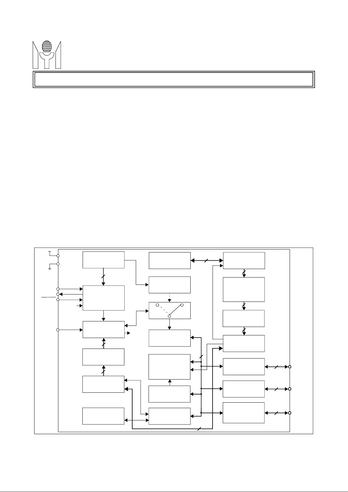
MTU8B5X series is an EPROM based 8-bit microcontroller which employs a full CMOS technology
enhanced with low-cost, high speed and high noise
immunity. W atchdog Timer, RAM, EPROM, tri-state
I/O port, power down mode, and real time programmable clock/counter are integrated into this chip.
MTU8B5X contains 33 instructions, all are single
cycle except for program branches which take two
cycles.
On chip memory is available with 512x14 bits of
EPROM for MTU8B54E/55E, 1Kx14 bits of EPROM
for MTU8B56E, 2Kx14 bits of EPROM for
BL OCK DIAGRAM
V
dd
V
ss
OSCI
OSCO
MCLR
T0CKI
Sleep
WDT/Timer0
Accumulator
Configuration
Word
Osc Mode
2
Select
Oscillator
Circuit
Prescaler
6
T0MODE
Register
6
Status
/Disable
Enable
WDT
Time Out
Four-level
Stack
WatchDog
Timer
Timer0
RAM
24, 25 or 27 Bytes
FSR
ALU
11
Data
8
8
Program
Counter
11
EPROM
2048 X 14
14
Instruction
Register
14
Instruction
Decoder
PortA
PortB
PortC
Only in MTU8B55E/57E
4
8
8
PB7:PB0
PC7:PC0
This datasheet contains new product information. Myson Technology reserves the rights to modify the product specification without
Revision 1.2 - 1 - 24 October 2000
e product.
Page 2
TECHNOLOGY
RC type: Input pin of RC oscillator
this pin is low, the device is reset.
In programmimg mode, this pin is connected to 12V. In normal operating
mode, this pin must not exceed Vdd to avoid entering unintended program-
PA0~PA3 as bi-directional I/O port
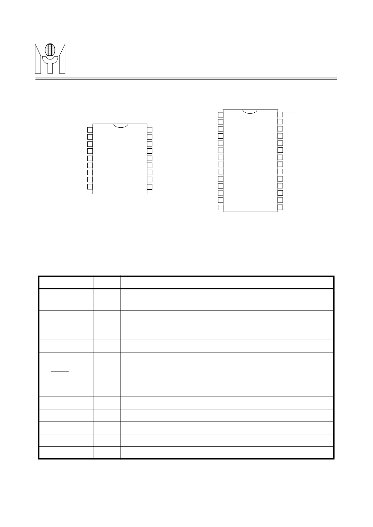
1.0 PIN CONNECTION
MTU8B54E/55E/56E/57EMYSON
PA2
PA3
T0CKI
MCLR/Vpp
Vss
PB0
PB1
PB2
PB3
1
2
3
4
MTU8B54E
5
MTU8B56E
6
7
8
9
2.0 PIN DESCRIPTIONS
Name I/O Descriptions
18
17
16
15
14
13
12
11
10
PA1
PA0
OSCI
OSCO
Vdd
PB7
PB6
PB5
PB4
T0CKI
Vdd
N/C
Vss
N/C
PA0
PA1
PA2
PA3
PB0
PB1
PB2
PB3
PB4
1
2
3
4
5
6
7
MTU8B55E
8
MTU8B57E
9
10
11
12
13
14
28
27
26
25
24
23
22
21
20
19
18
17
16
15
MCLR/Vpp
OSCI
OSCO
PC7
PC6
PC5
PC4
PC3
PC2
PC1
PC0
PB7
PB6
PB5
OSCI I
OSCO O
T0CKI/SCL I Input pin of real time counter/clock. Must be tied to Vss or Vdd if not in use.
MCLR/Vpp I
PA0~PA3 I/O
PB0~PB7 I/O PB0~PB7 as bi-directional I/O port
PC0~PC7 I/O PC0~PC7 as bi-directional I/O port
Vdd - Power supply
Vss - Ground
XTAL type: Input terminal of crystal oscillator
RC type: OSCO outputs with 1/4 frequency of OSCI to denotes the cycle
rate for instruction.
XTAL type: Output terminal of crystal oscillator
Input pin for device reset or high voltage programming input for EPROM. If
ming mode.
Revision 1.2 - 2 - 24 October 2000
Page 3

TECHNOLOGY
3.0 FUNCTIONAL DESCRIPTIONS
The Regis ter Map of MTU8B54E/56E
The Regist er Map of MTU8B55E
The Regi ster Map of MTU8B57E
Map back to address in Bank 0
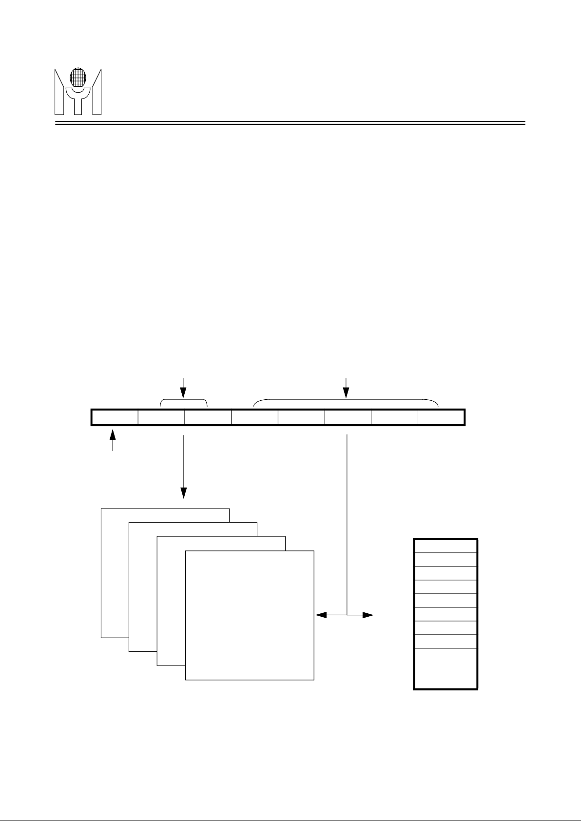
3.1 REGISTER MAP
The register map of MTU8B5X is depicted as below:.
MTU8B54E/55E/56E/57EMYSON
Address Description
00h Indirect Addressing Register
01h Timer0
02h PC
03h STA TUS
04h FSR
05h PORTA
06h PORTB
07h-1Fh General Purpose Register
Address Description
FSR<6:5>
00h
Bank 0
00
Indirect Addressing Register
Bank 1
01
Address Description
00h Indirect Addressing Register
01h Timer0
02h PC
03h STATUS
04h FSR
05h PORTA
06h PORTB
07h PORTC
08h-1Fh General Purpose Register
Bank 2
10
Bank 3
11
01h Timer0
02h PC
03h STATUS
04h FSR
05h PORTA
06h PORTB
07h PORTC
08h~0Fh
Revision 1.2 - 3 - 24 October 2000
General Purpose
Register
10h~1Fh
General Purpose
Register
30h~3Fh
General Purpose
Register
50h~5Fh
General Purpose
Register
70h~7Fh
General Purpose
Register
Page 4
MTU8B54E/55E/56E/57EMYSON
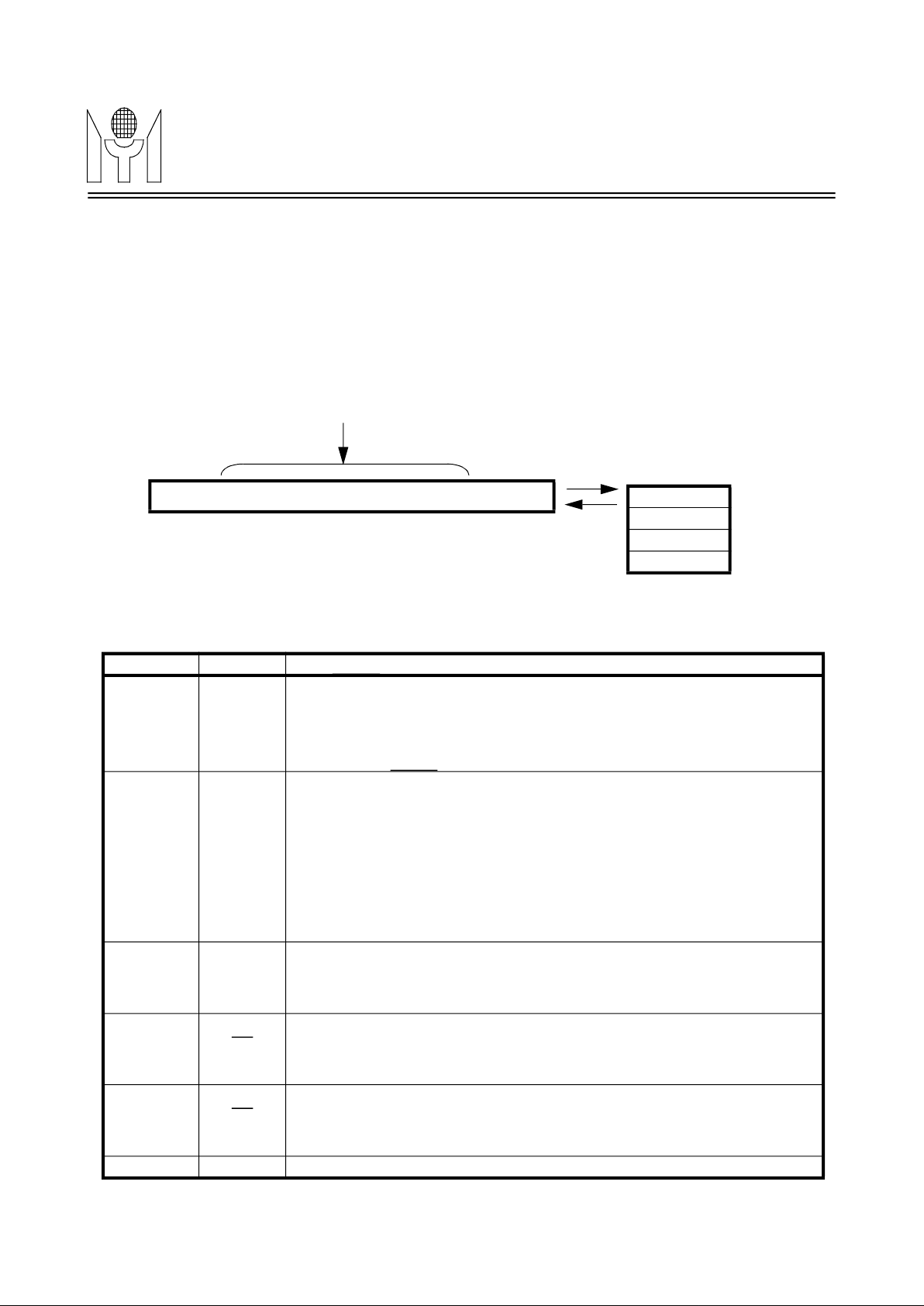
INA R(Indir ect Ad d res s Regist er) : R0
R0 is not a physically implemented register. It is used a s an indirect addressing pointer. Any instruction
accessing this register can access data pointed by FSR(R4).
This register increases by an external signal edge applied to T0CKI pin, or by internal instruction cycle. It can
be read or written as any other register.
STATUS(Status Regis t er ):
The content of R3 is listed in Table 1.
LCALL, LGOTO : from instruction word
RETIA : from STACK
TABL E 1. STATUS Regis ter
= 1, a carry occurred = 1, a borrow did not occur
Half carry/half
= 0, a carry from the 4th low order bit of the result did not occur
= 1, the result of a logic operation is zero
Power down flag bit:
= 0, by the SLEEP instruction
Time overflow flag bit:
= 0, a WDT time-overflow occurred
TECHNOLOGY
3.1.1
3.1.2 Timer0(8-bit real-time cl o ck /ti m er) : R1
3.1.3 PC(Pro g r am Coun ter) : R2
This register increases itself every instruction cycle, except the following condition shown in Figure 1:
LCALL
A10~A0
RETIA
FIGURE 1. Pr o g ram Counter
Stack1
Stack2
Stack3
Stack4
3.1.4
Bit Symbol Description
Carry/borrow bit
0 C
1 DC
2 Z
3 PD
ADDWF SUBWF
= 0, a carry did not occur = 0, a borrow occurred
borrow bit
ADDWF
= 1, a carry from the 4th low order bit of the result occurred
SUBWF
= 1, a borrow from the 4th low order bit of the result did not occur
= 0, a borrow from the 4th low order bit of the result occurred
Zero bit:
= 0, the result of a logic operation is not zero
= 1, after power-up or by the CLRWDT instruction
4 TO
5, 6, 7 - Unused
Revision 1.2 - 4 - 24 October 2000
= 1, after power-up or by the CLRWDT or SLEEP instruction
Page 5
TECHNOLOGY
Bit 0~4 are used to select up to 32 registers (address: 00h~1Fh) and Bit 5~6 are Bank Select (Bank0~3) in the
PA3:PA0, bi-directional I/O Register
T0MODE REGISTER:
T0MODE is a write-only register and the content is listed in Table 2.
= 0, I/O pin in output mode;
= 1, I/O pin in input mode.
FIGURE 2. Data Memory Conf i g u raion
Timer0
STA TUS
PORT A
PORT B
8 Bytes
3.1.5 FSR(File select regi st er po i n t er): R4
indirect addressing mode shown in Figure 2.
3.1.6 PORT A: R5
3.1.7 PORT B: R6
PB7:PB0, bi-directional I/O Register
3.1.8 PORT C: R7
PB7:PB0, bi-directional I/O Register, and for MTU8B55E/57E only
3.1.9
3.1.10 IOST (Contr o l Por t I/O Mode Regist er)
The IOST register is “write-only”
MTU8B54E/55E/56E/57EMYSON
Bank Select
B7 B6 B5 B4 B3 B2 B1 B0
Read 1
70h
7Fh
50h
5Fh
Bank 3
30h
3Fh
Bank 2
Bank 1
Bank 0
16 Bytes
SRAM
Indirect Addressing Mode
Location Select
00h INAR
10h
1Fh
01h
02h PC
03h
04h FSR
05h
06h
07h PORT C
08h
0Fh
SRAM
Bank 0
Revision 1.2 - 5 - 24 October 2000
Page 6

MTU8B54E/55E/56E/57EMYSON
TABLE 2. T0MODE Regi ster
Timer Rate
WDT Rate
Timer0 source signal edge select bit:
= 1, increment when high-to-low transition on T0CKI pin
Timer0 source signal select bit:
= 0, internal instruction clock cycle
TECHNOLOGY
Bit Symbol Description
Bit Value
2-0 PS2:PS0
Prescaler assign bit:
3 PSC
4 TE
5 TS
6, 7 - Unused
= 0, Timer0
= 1, WDT
= 0, increment when low-to-high transition on T0CKI pin
= 1, transition on T0CKI pin
0 0 0
0 0 1
0 1 0
0 1 1
1 0 0
1 0 1
1 1 0
1 1 1
1:2
1:4
1:8
1:16
1:32
1:64
1:128
1:256
1:1
1:2
1:4
1:8
1:16
1:32
1:64
1:128
Revision 1.2 - 6 - 24 October 2000
Page 7

TECHNOLOGY
Affected
Test bit in R and skip if clear
Test bit in R and skip if set
Clear Watchdog Timer
Go into standby mode
Load IOST Register
AND immediate with Acc
Exclusive OR immediate with Acc
Move immediate to Acc
Inclusive OR immediate with Acc
Return, place immediate in A
Complement R
Increment R, Skip if 0
3.2 INSTRUCTION SET
MTU8B54E/55E/56E/57EMYSON
Mnem oni c
Instruction
Status
Descr ipti on Cycl es
Operands
BCR R, bit Clear bit in R 1 11 11bb brrr rrrr None
BSR R, bit Set bit in R 1 11 10bb brrr rrrr None
BTRSC R, bit
BTRSS R, bit
CLRWDT
T0MODE Load T0MODE Register 1 01 0000 0000 0010 None
SLEEP
IOST R
ANDIA I
XORIA I
MOVIA I
IORIA I
1 or
2(skip)
1 or
2(skip)
1 01 0000 0000 0001 TO, PD
1 01 0000 0000 0011 TO, PD
1 01 0000 0000 0rrr None
1 00 1001 iiii iiii Z
1 00 1000 iiii iiii Z
1 00 0001 iiii iiii None
1 00 0011 iiii iiii Z
11 01bb brrr rrrr None
11 00bb brrr rrrr None
Code
RETIA I
LCALL I Call subroutine 2 10 0iii iiii iiii None
LGOTO I Unconditional branch 2 10 1iii iiii iiii None
NOP No operation 1 01 0000 0000 0000 None
MOVAR R Move Acc to R 1 01 0000 1rrr rrrr None
COMR R, d
MOVR R Move R 1 01 0011 drrr rrrr Z
RRR R, d Rotate right R 1 01 1110 drrr rrrr C
RLR R, d Rotate left R 1 01 1100 drrr rrrr C
SWAPR R, d Swap halves R 1 01 1101 drrr rrrr None
CLRA Clear Acc 1 01 0001 0000 0000 Z
CLRR R Clear R 1 01 0001 1rrr rrrr Z
INCR R, d Increment R 1 01 1000 drrr rrrr Z
INCRSZ R, d
2 00 1100 iiii iiii None
1 01 0010 drrr rrrr Z
1 or
2(skip)
01 1001 drrr rrrr None
Revision 1.2 - 7 - 24 October 2000
Page 8

TECHNOLOGY
3.3 I/O PORTS EQUIVALENT CIRCUIT
WDT : Watchdog Timer
i : Immediate data
T0MODE : T0MODE register
: Time overflow bit
IOST : I/O port status register
DC : Digital carry flag
If d is “0”, the result is stored in the Acc register.
If d is “1”, the result is stored back in register R.
Affected
Decrement R, Skip if 0
Note : 1. The IOST registers are “write-only” and set upon RESET.
if the IOST latch is “1”, the corresponding I/O pin is in input mode.
MTU8B54E/55E/56E/57EMYSON
Mnem oni c
Descr ipti on Cycl es
Operands
DECR R, d Decrement R 1 01 0110 drrr rrrr Z
DECRSZ R, d
SUBAR R, d Subtract Acc from R 1 01 1010 drrr rrrr C, DC, Z
XORAR R, d Exclusive OR Acc with R 1 01 1011 drrr rrrr Z
ANDAR R, d AND Acc with R 1 01 0100 drrr rrrr Z
ADDAR R, d Add Acc and R 1 01 0101 drrr rrrr C, DC, Z
IORAR R, d Inclusive OR Acc with R 1 01 1111 drrr rrrr Z
Note: b : Bit position
Acc : Accumulator
PD : Power down flag TO
Z : Zero flag C : Carry flag
I : (i7i6i5i4i3i2i1i0) R : (r6r5r4r3r2r1r0)
d 01,[ ]∈
:Destination
1 or
2(skip)
Instruction
Status
Code
01 0111 drrr rrrr None
R : Register address
Acc Data
IOST R
Data Bus
WR Port
2. If the IOST latch is “0”, the corresponding I/O pin is in output mode;
D
IOST
Latch
CK
D
Data
Latch
CK
QB
QB
Q
Q
RD Port
VDD
VSS
I/O Pin
Revision 1.2 - 8 - 24 October 2000
Page 9

MTU8B54E/55E/56E/57EMYSON
reset (normal operation).
(3) WDT reset (normal operation).
wake-up (from sleep mode).
(5) WDT wake-up (from sleep mode) : Executing the SLEEP instruction can force this device entering into
sleep mode (power saving mode). While in sleep mode, the WDT is cleared but keeps running. This
Note: x = unknown, u = unchanged, - = unimplemented, read as “0”,
Power-On Reset
/MCLR or WDT Reset
111 1 1111
111 1 11 11
111 1 1111
111 1 11 11
--1 1 11 1 1
WDT Reset (not during SLEEP)
WDT Reset during SLEEP
TECHNOLOGY
3.4 RESET
This device may be reset by one of the following ways:
(1) Power-on Reset : At power-up, this device will be kept in a RESET condition for a period of 18ms after
the voltage on MCLR/Vpp pin has reached a logic high level.
(2) MCLR
(4) MCLR
device can be awakened by WDT time-out or reset input on MCLR pin.
The contents of registers after reset are listed below:
Address Register
00h INAR xxxx xxxx uuuu uuuu
01h Timer0 xxxx xxxx uuuu uuuu
02h PC
03h STATUS 0001 1xxx 000# #uuu
04h FSR 1xxx xxxx 1uuu uuuu
05h PORTA ---- xxxx ---- uuuu
06h PORTB xxxx xxxx uuuu uuuu
07h PORTC xxxx xxxx uuuu uuuu
07h-1Fh General Purpose Register xxxx xxxx uuuu uuuu
N/A Acc xxxx xxxx uuuu uuuu
N/A IOST
N/A T0MODE --11 11 1 1
# = refer to the following table
Condition Status:bit 4 Status:bit 3
/MCLR Reset (not during SLEEP) u u
/MCLR Reset during SLEEP 1 0
0 1
0 0
Revision 1.2 - 9 - 24 October 2000
Page 10

MTU8B54E/55E/56E/57EMYSON
Timer0 is an 8-bit timer/counter. The clock source of T imer0 can come from the internal clock or by an external
To select the internal clock source, bit 5 of the T0MODE register should be reset. In this mode, Timer0 will
To select the external clock source, bit 5 of the T0MODE register should be set. In this mode, Timer0 will
Wat c h dog Timer (WDT)
The Watchdog Timer is a free running on-chip RC oscillator. This RC oscillator is separated from the RC oscil-
as in sleep mode. During normal operation or in sleep mode, a WDT time-out will cause the device reset and
Without prescaler, the WDT time-out period is 18ms. This period can be increased by using the prescaler . The
the Timer0. The PS2:PS0 bits determine the prescale ratio. When assigned to Timer0, the prescaler will be
cleared by instructions which write to Timer0 Register. A CLRWDT instruction will clear the WDT and pres-
caler when assigned to WDT. The prescaler can not be assigned to both the Timer0 and WDT simultaneously.
WDT enable
WDT Time-Out
TECHNOLOGY
3.5 REAL TIME CLOCK (TIMER0) AND WATCHDOG TIMER
T0CKI
F
TE
OSC
/4
1
M
U
0
X
TS
PSC
1
MUX
0
PSC
0
WDT
1
MUX
Sync
2 cycles
Timer0
8 bits
Data Bus
3.5.1 Timer0
clock source presented at the T0CKI pin.
increase by 1 in every instruction cycle (without prescaler).
increase by 1 on every falling or rising edge of T0CKI pin is controlled by bit 4 of T0MODE register.
PS2:PS0
8-bit prescaler
PSC
8 bits
8-to-1 MUX
1
0
MUX
3.5.2
lator of the OSCI pin. That means the WDT will keep running even when the oscillator driver is turned off, such
the TO bit (bit 4 of STATUS register) will be cleared.
division ratio of prescaler is up to 1:128. Thus, the longest time-out period is approximately 2.3s.
3.5.3 Pr esc aler
The 8-bit prescaler may be assigned to either the Timer0 or the WDT through the PSC bit (bit 3 of the
T0MODE register). Setting this bit assigns the prescaler to the WDT. Resetting this bit assigns the prescaler to
Revision 1.2 - 10 - 24 October 2000
Page 11

MTU8B54E/55E/56E/57EMYSON
3.6 OSCILLATOR CONFIGURATION
mode. These oscillator modes offered as:
• RC: Low-cost crystal
• XTAL: Standard crystal oscillator
XTAL, HFXTA L or LFXTAL m odes
3.7 CONFIGURATION WORD
external system
Watchdog Timer enable
Watchdog Timer disable
TECHNOLOGY
This device supports four oscillator modes. Users can program two configuration bits to select the appropriate
• HFXTAL: High frequency crystal oscillator
• LFXTAL: Low frequency crystal oscillator
3.6.1
MTU8B54E/55E/56E/57E
Internal
Circuit
SLEEP
MTU8B54E/55E/56E/57E
OSCI
C
1
(a) Crys t al Operatio n (or Ceramic Resonato r )
3.6.2 RC Osc il l ator Mode
R
C
Bit 3
Code Protect
1
0
x
x
x
x
x
x
Bit2
WDT Enable
x
x
1
0
x
x
x
x
OSCO
RF
XTAL
OSCO
Oscillator Type
OSCI
RS
C
Bit1
x
x
x
x
1
1
0
0
2
(b) Ext ernal Clock Input Operation
MTU8B54E/55E/56E/57E
internal
clock
0 4÷
Bit0
Oscillator Type
x
x
x
x
1
0
1
0
EPROM unprotected
EPROM protected
RC
HFXTAL
XTAL
LFXTAL
OSCI
Clock from
Function Remark
OSCO
Open
Default
Default
Default
Revision 1.2 - 11 - 24 October 2000
Page 12

MTU8B54E/55E/56E/57EMYSON
4.0 ABSOLUTE MAXIMUM RATINGS
Ambient Operating Temperature
Store T emperature
DC Supply Voltage(V
Voltage with respect to Ground(V
5.0 OPERATING CONDITIONS
DC Supply Voltage
Operaing Temprature
6.0 ELECTRICAL CHA RACTERISTICS
=-5.4mA,
=8.7mA in RC mode
WDT Enable, V
WDT Disable, V
HFXTAL: 24MHz, WDT Disable
LFXTAL: 32kHz, WDT Disable
XTAL: 12MHz, WDT Disable
TECHNOLOGY
-55oC to +125oC
-65oC to +150oC
) 0V to +7.5V
dd
) 0.6V to (Vdd + 0.6)V
ss
Voltage on MCLR(Vpp) with respect to Ground(Vss) 0V to +12V
+2.3V to +6.5V
-40oC to +85oC
(Under Operating Conditions)
6.1 ELECTRICAL CHARACTERISTICS of MTU8B54E/56E
Parameter Sym Min. Typ. Max. Units Conditions
Input High Voltage
Input Low Volatge
Output Voltage
Sleep Current
V
IH
V
IL
V
Oh
V
OL
I
PD
I
PD
3.8 V I/O Ports, Vdd=4.5V, I
2.2 V
4.2 V
1.1 V
1.0 V
0.6 V
3.0 uA
<1 uA
I/O ports, Vdd=5V
MCLR, Vdd=5V
I/O ports, Vdd=5V
MCLR, Vdd=5V
I
ol
=3.0V
dd
dd
oh
=3.0V
8.07 mA
I
DD
I
I
DD
DD
Operating Current
Revision 1.2 - 12 - 24 October 2000
5.16 mA
3.98 mA
2.05 mA
2.8 mA
1.77 mA
1.31 mA
604 uA
224 uA
88 uA
6.21 mA
3.91 mA
2.71 mA
1.39 mA
685 uA
Vdd=6.4V
Vdd=5.0V
Vdd=4.0V
Vdd=3.0v
Vdd=6.4V
Vdd=5.0V
Vdd=4.0V
Vdd=3.0V
Vdd=2.4V
Vdd=2.1V **
Vdd=6.4V
Vdd=5.0V
Vdd=4.0V
Vdd=3.0V
Vdd=2.4V
Page 13

MTU8B54E/55E/56E/57EMYSON
XTAL: 4MHz, WDT Disable
Vdd=5V, RC mode, WDT Disable, These
F=617kHz
R=100kOhm
F=311kHz
R=300kOhm
F=403kHz
R=100kOhm
F=202kHz
R=300kOhm
F=676kHz
F=154kHz
R=100kOhm
R=300kOhm
F=617kHz
F=313kHz
R=100kOhm
R=300kOhm
TECHNOLOGY
Parameter Sym Min. Typ. Typ. Units Conditions
5.01 mA
Operating Current
I
DD
3.03 mA
2.05 mA
916 uA
391 uA
195 uA
6.32 mA
3.11 mA R=4.7kOhm F=4.10MHz
2.46 mA R=10kOhm F=2.38MHz
1.88 mA R=47kOhm
1.80 mA
1.73 mA
6.18 mA
2.91 mA R=4.7kOhm F=2.98MHz
2.31 mA R=10kOhm F=1.67MHz
1.84 mA R=47kOhm
Vdd=6.4V
Vdd=5.0V
Vdd=4.0V
Vdd=3.0V
Vdd=2.1V **
values include current through Rext
R=900Ohm F=7.80MHz
C=3P
F=103Hz
R=900Ohm F=6.76MHz
C=20P
1.77 mA
I
DD
** Operating at Vdd=2.1V is for reference only.
1.72 mA
5.72 mA
2.60 mA R=4.7kOhm F=1.33MHz
2.13 mA R=10kOhm
1.79 mA R=47kOhm
1.75 mA
1.71 mA
5.32 mA
2.45 mA R=4.7kOhm
2.06 mA R=10kOhm
1.78 mA R=47kOhm F=64.9kHz
1.74 mA
1.71 mA
F=65.8kHz
R=900Ohm F=4.17MHz
C=101P
F=75.8kHz
F=24.5kHz
R=900Ohm F=2.34MHz
C=301P
F=32.5kHz
F=10.4kHz
Revision 1.2 - 13 - 24 October 2000
Page 14

MTU8B54E/55E/56E/57EMYSON
mA in RC mode
WDT Enable, V
WDT Disable, V
HFXTAL: 24MHz, WDT Disable
LFXTAL: 32kHz, WDT Disable
XTAL: 12MHz, WDT Disable
XTAL: 4MHz, WDT Disable
TECHNOLOGY
6.2 ELECTRICAL CHARACTERISTICS of MTU8B55E/57E
Parameter Sym Min. Typ. Max. Units Conditions
Input High Voltage
Input Low Volatge
Output Voltage
Sleep Current
V
IH
V
IL
V
Oh
V
OL
I
PD
I
PD
3.8 V
2.2 V
4.2 V
1.1 V
1.0 V
0.6 V
3.0 uA
<1 uA
I/O ports, Vdd=5V
MCLR, Vdd=5V
I/O ports, Vdd=5V
MCLR, Vdd=5V
I/O Ports, Vdd=4.5V, Ioh=-5.4mA,
Iol=8.7
=3.0V
dd
dd
=3.0V
Operating Current
I
I
I
DD
DD
DD
8.87 mA
5.84 mA
4.09 mA
1.88 mA
2.83 mA
1.96 mA
1.42 mA
675 uA
279 uA
116 uA
6.70 mA
4.39 mA
3.12 mA
1.76 mA
908 uA
mA
3.11 mA
2.22 mA
1.17 mA
578 uA
377 uA
Vdd=6.4V
Vdd=5.0V
Vdd=4.0V
Vdd=3.0v
Vdd=6.4V
Vdd=5.0V
Vdd=4.0V
Vdd=3.0V
Vdd=2.4V
Vdd=2.1V **
Vdd=6.4V
Vdd=5.0V
Vdd=4.0V
Vdd=3.0V
Vdd=2.4V
Vdd=6.4V
Vdd=5.0V
Vdd=4.0V
Vdd=3.0V
Vdd=2.1V **
Revision 1.2 - 14 - 24 October 2000
Page 15

MTU8B54E/55E/56E/57EMYSON
Vdd=5V, RC mode, WDT Disable, These
F=56.8kHz
F=73.1kHz
F=23.6kHz
F=311kHz
F=66.8kHz
F=32.7kHz
F=10.5kHz
TECHNOLOGY
Parameter Sym Min. Typ. T yp. Units Conditions
values include current through Rext
6.58 mA
3.18 mA R=4.7kOhm F=3.85MHz
2.55 mA R=10kOhm F=2.10MHz
2.05 mA R=47kOhm F=500kHz
1.98 mA R=100kOhm F=250kHz
1.93 mA R=300kOhm F=82.8Hz
6.40 mA
3.03 mA R=4.7kOhm F=2.86MHz
2.46 mA R=10kOhm F=1.52MHz
2.04 mA R=47kOhm F=352kHz
Operating Current
** Operating at Vdd=2.1V is for reference only.
I
DD
1.97 mA R=100kOhm F=176kHz
1.93 mA R=300kOhm
5.90 mA
2.79 mA R=4.7kOhm F=1.33MHz
2.34 mA R=10kOhm F=676kHz
2.02 mA R=47kOhm F=147kHz
1.97 mA R=100kOhm
1.93 mA R=300kOhm
5.48 mA
2.60 mA R=4.7kOhm F=638kHz
2.28 mA R=10kOhm
2.02 mA R=47kOhm
1.98 mA R=100kOhm
1.93 mA R=300kOhm
C=3P
C=20P
C=101P
C=301P
R=900Ohm F=9.12MHz
R=900Ohm F=7.72MHz
R=900Ohm F=4.61MHz
R=900Ohm F=2.46MHz
Revision 1.2 - 15 - 24 October 2000
Page 16

MTU8B54E/55E/56E/57EMYSON
7.0 PACKAGE DIMENSION
TOP E-PIN INDENT
BOTTOM E-PIN INDENT
Dimension In Millemeters
Dimension In Inches
TECHNOLOGY
7.1 18 Pin PDIP 300mil f or MTU8B54EN and MTU8B56EN
D
E1
(4x)
o
E
15
eB
0.727
A
L
e
Symbols
A - - 4.57 - - 0.180
A1 0.13 - - 0.005 - A2 - 3.30 3.56 - 0.130 0.140
B 0.36 0.46 0.56 0.014 0.018 0.022
B1
Min Nom Max Min Nom Max
B
A2
A1
D1
∅0.079
∅0.118
C
B1 1.27 1.52 1.78 0.050 0.060 0.070
C 0.20 0.25 0.33 0.008 0.010 0.013
D 22.71 22.96 23.11 0.894 0.904 0.910
D1 0 .43 0.56 0.69 0.017 0.022 0.027
E 7.62 - 8.26 0.300 - 0.325
E1 6.40 6.50 6.65 0.252 0.256 0.262
e - 2.54 - - 0.100 L 3.18 - - 0.125 - -
eB 8.38 - 9.65 0.330 - 0.380
Revision 1.2 - 16 - 24 October 2000
Page 17

MTU8B54E/55E/56E/57EMYSON
Dimension In Millimeters
Dimension In Inches
TECHNOLOGY
7.2 18 Pi n SOP for MTU8B54EP and MTU8B56EP
E
H
(4x)
o
7
o
view “A”
0.020x45
D
7o(4x)
A
A2
B
Symbols
Min Nom Max Min Nom Max
A 2.36 2.49 2.64 0.093 0.098 0.104
A1 0.10 - 0.30 0.04 - 0.012
A2 - 2.31 - - 0.091 -
B 0.33 0.41 0.51 0.013 0.016 0.020
C 0.18 0.23 0.28 0.007 0.009 0.011
e
A1
view “A”
C
L
θ
D 11.35 - 1 1.76 0.447 - 0.463
E 7.39 7.49 7.59 0.291 0.295 0.299
e - 1.27 - - 0.050 -
H 10.01 10.31 10.64 0.394 0.406 0.419
L 0.38 0.81 1.27 0.015 0.032 0.050
o
θ
Revision 1.2 - 17 - 24 October 2000
0
-
0
8
o
0
-
o
8
Page 18

MTU8B54E/55E/56E/57EMYSON
Dimension In Millimeters
TECHNOLOGY
7.3 28 Pin PDIP 300mil f or MTU8B55EM and MTU8B57EM
D
E1
(4x)
o
E
15
eB
PIN 1 INDENT
A
L
Symbols
A - - 4.57 - - 0.180
A1 0.38 - - 0.015 - A2 - 3.30 3.56 - 0.130 0.140
B 1.02 - 1.65 0.0040 - 0.065
1.000”
A2
A1
e
B1
Min Nom Max Min Nom Max
B
B2
Dimension In Inches
C
B1 0.41 - 0.58 0.016 - 0.023
B2 0.71 - 1.12 0.028 - 0.044
C 0.20 0.25 0.33 0.008 0.010 0.013
D 3 5.13 35.18 35.43 1.383 1.385 1.395
E 7.87 8.31 8.38 0.310 0.327 0.330
E1 7.26 7.32 7.52 0.284 0.288 0.296
e - 2.54 - - 0.100 -
L 3.18 - - 0.125 - eB 8.64 - 9.65 0.340 - 0.380
Revision 1.2 - 18 - 24 October 2000
Page 19

MTU8B54E/55E/56E/57EMYSON
Dimension In Millimeters
TECHNOLOGY
7.4 28 Pin PDIP 600mil f or MTU8B55EN and MTU8B57EN
D
E1
(4x)
o
15
E
eB
A
L
A2
A1
e
Symbols
A - - 5.59 - - 0.220
A1 0.38 - - 0.015 - A2 3.81 3.94 4.06 0.150 0.155 0.160
B - 1.52 - - 0.06 B1 - 0.46 - - 0.018 -
D 3 6.96 37.08 37.34 1.455 1.460 1.470
E - 15.24 - - 0.600 -
B1
Min Nom Max Min Nom Max
B
Dimension In Inches
E1 13.72 13.84 13.97 0.540 0.545 0.550
e - 2.54 - - 0.100 -
L 3.18 - - 0.125 - eB 16.00 16.51 17.02 0.630 0.650 0.670
Revision 1.2 - 19 - 24 October 2000
Page 20

MTU8B54E/55E/56E/57EMYSON
Dimension In Millimeters
Dimension In Inches
TECHNOLOGY
7.5 28 Pi n SOP for MTU8B55EP and MTU8B57EP
E
eB
(4x)
o
7
o
view “A”
0.020x45
D
A2
view “A”
A
7o(4x)
e
D1
B
Symbols
Min Nom Max Min Nom Max
A - 2.488 2.743 - 0.098 0.108
A1 0.152 - - 0.006 - A2 2.21 2.336 2.464 0.087 0.091 0.097
B 0.305 0.406 0.508 0.012 0.016 0.020
C 0.204 0.254 0.304 0.008 0.010 0.012
A1
C
θ
L
D 17.78 17.91 18.42 0.700 0.705 0.725
E 7.366 7.493 7.62 0.290 0 .295 0.300
e 1.219 1.270 1.321 0.048 0.050 0.052
eB 10.26 10.42 10.57 0.404 0.410 0.416
L 0.635 - - 0.025 - -
o
θ
D1 0.356 0.508 - 0.0 14 0.020 -
Revision 1.2 - 20 - 24 October 2000
0
o
4
0
8
o
0
o
4
o
8
Page 21

MTU8B54E/55E/56E/57EMYSON
8.0 PAD ASSIGNMENT
Pad size : 110um x 110um
TOCKI/SCL
TECHNOLOGY
8.1 Pad As sig nmemt f or MTU8B54E an d MTU8B56E
pp
18
MCLR/V
Vss
TOCKI/SCL
151617
PA2
PA3/SDA
1314
PA0
PA1
12
OSCO
OSCI
1011
Pad of MTU8B54E/56E
Chip size : 1710um x 1760um
1 2
PB0
Pad No. Pad X Y Pad No. Pad X Y
1 PB0 145.45 153.05 10 OSCO 1598.95 1606.95
3 4 5
PB1
PB2
PB3
PB4
6 7
PB5
8
9
PB6
PB7
Vdd
2 PB1 320.95 153.05 11 OSCI 1264.95 1606.95
3 PB2 496.45 153.05 12 PA0 1098.45 1606.95
4 PB3 671.95 153.05 13 PA1 922.95 1606.95
5 PB4 847.45 153.05 14 PA2 747.45 1606.95
6 PB5 1022.95 153.05 15 PA3/SDA 571.95 1606.95
7 PB6 1198.45 153.05 16
8 PB7 1373.95 153.05 17
9
Revision 1.2 - 21 - 24 October 2000
V
dd
1557.45 153.05 18
MCLR/V
V
ss
424.90 1606.95
249.20 1606.95
pp
124.20 1606.95
Page 22

MTU8B54E/55E/56E/57EMYSON
Pad size : 110um x 110um
2117.01
TOCKI/SCL
1 127.60
TECHNOLOGY
8.2 Pad As sig nment f or MTU8B55E an d MTU8B57E
pp
dd
V
20
V
ss
PA0
PA1
PA2
PA3
PB0
Pad No. Pad X Y Pad No. Pad X Y
21 22
23 24 25
26
1 2
PB1
T0CKI/SCL
MCLRB/V
1819
Pad of MTU8B55E/57E
Chip size : 2201um x 1822um
3 4 5 6 7
PB2
PB3
OSCI
17
PB4
PB5
PB6
PC7
OSCO
1516
PC6
1413
PC5
PC4
1211109
PC3
PC2
8
PC0
PB7
PC1
1 PB1 217.01 93.20 14 PC6
2 PB2 476.09 93.20 15 PC7 1830.89 1738.75
3 PB3 720.67 93.20 16 OSCO 1595.29 1733.20
4 PB4 979.75 93.20 17 OSCI 1210.68 1733.20
5 PB5 1224.33 93.20 18
6 PB6 1483.41 93.20 19
7 PB7 1727.99 93.20 20
8 PC0 1987.07 93.20 21
9
10 PC2 2117.01 620.48 23 PA1 93.21
11 PC3 2117.01 865.06 24 PA2 93.21 868.52
12 PC4 2117.01 1124.14 25 PA3/SDA 93.21 623.94
13 PC5 2117.01 1386.72 26 PB0 93.21 364.86
PC1
2117.01 361.40 22 PA0 93.21 1372.18
MCLR/V
V
dd
V
ss
863.95 1738.79
pp
603.04 1738.75
344.41 1738.75
101.98 1644.97
1627.80
Revision 1.2 - 22 - 24 October 2000
Page 23

MTU8B54E/55E/56E/57EMYSON
TECHNOLOGY
9.0 Order Infor m ati o n
Type 300mil PDIP 600mil PDIP 300mil SOP Die Form
18pins MTU8B54EN - MTU8B54EP MTU8B54E
28pins MTU8B55EM MTU8B55EN MTU8B55EP MTU8B55E
18pins MTU8B56EN - MTU8B56EP MTU8B56E
28pins MTU8B57EM MTU8B57EN MTU8B57EP MTU8B57E
Revision 1.2 - 23 - 24 October 2000
 Loading...