

Page 1
MYSON
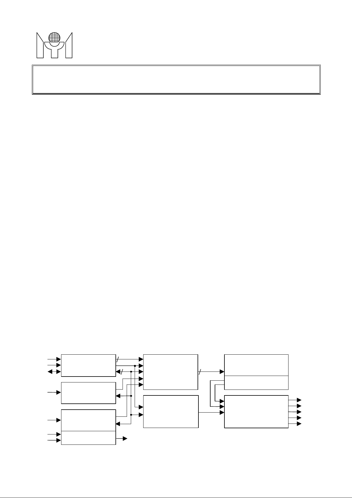
SERIAL DATA
VERTICAL
HORIZONTAL
DISPLAY & ROW
(RAM)
FONTS ROM &
WINDOWS & FRAME
LUMINANCE & BORDER
GENERATOR
HFLB
VFLB
VCORPSSB
SCK
SDA
ROUT
GOUT
BOUT
FBKG
INT
SHADOW
WINDOW
MTV048
TECHNOLOGY
(Rev 0.9)
On-Screen-Display Controller
for CRT/LCD Monitor
FEATURES
• Software control for CRT/LCD applications.
• Full screen self-test pattern generator with programmable pattern color.
• On-chip PLL circuitry (CRT) or external pixel clock input (LCD) up to 150 MHz.
• Horizontal SYNC input up to 150 KHz.
• Programmable horizontal resolutions up to 1524 dots per display line.
• Full screen display consists of 15 (rows) by 30 (columns).
• 12x16 or 12x18 dot matrix selection.
• A total of 384 fonts including 360 standard fonts, 16 multi-color fonts and 8 user fonts.
• 8 color selections for character foreground, background and window color.
• Character button boxes with programmable box length.
• Character bordering, shadowing and blinking effect for display.
• Full-screen character double width control.
• Double character height and/or width control per row.
• Programmable positioning for display screen center.
• Row to row spacing control per row to avoid expansion distortion.
• 4 programmable background windows with multi-level operation and programmable shadow width/height/color.
• Software clear bit for full-screen erasing.
• Programmable adaptive approach to handle H, V sync collision automatically by hardware.
• Fade-in/fade-out or blend-in/blend-out effects.
• Compatible with SPI bus or I
• 5V or 3.3V power supply.
• 16-pin PDIP/SOP package.
2
C interface with address 7AH (slave address is mask option).
GENERAL DESCRIPTION
MTV048 is designed for monitor applications to display built-in fonts onto monitor screens. The display operation
occurs by transferring data and controls information from the micro controller to RAM through a serial data
interface. It can execute a full-screen display automatically, as well as specific functions such as character
background, bordering, shadowing, blinking, double height and width, font-by-font color control, button boxes,
frame positioning, frame size control by character height and row-to-row spacing, horizontal display resolution, fullscreen erasing, fade-in/fade-out effect, windowing effect, shadowing on window and full-screen self-test pattern
generator.
MTV048 provides 384 fonts including 360 standard fonts, 16 multi-color fonts and 8 user fonts and 2 font sizes,
12x16 or 12x18 for more efficacious applications. The full OSD menu is formed by 15 rows x 30 columns, which
can be positioned anywhere on the monitor screen by changing vertical or horizontal delay.
BL OCK DIAGRAM
9 RAMADDR
INTERFACE
DISPLAY CONTROL
DISPLAY CONTROL
R/WEN
8 DATA
ROW
COLUMN
CONTROL
REGISTERS
CONTROL
9 ROMADDR
USER FONTS RAM
LUMA
COLOR ENCODER
This datasheet contains new product information. Myson Technology reserves the rights to modify the product specification without
notice. No liability is assumed as a result of the use of this product. No rights under any patent accompany the sale of the product.
Rev 0.9 - 1 - 2001/03/15
PHASE LOCK LOOP
VCLK
Page 2
MYSON
This ground pin is used for internal analog circuitry.
inside. The frequency of XIN must be the integral time of pin HFLB.
internal display registers and control registers. It has an internal pull-
Positive 5V / 3.3V DC supply for internal
MTV048N-xx
MTV048
TECHNOLOGY
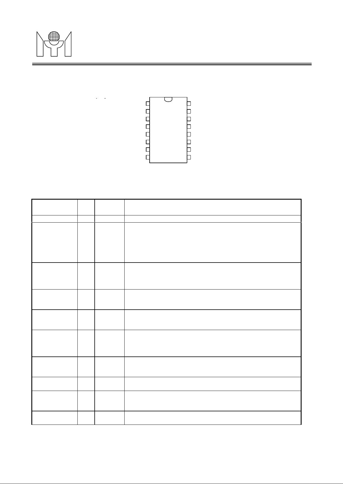
1.0 PIN CONNECTION
VSSA
VCO/XIN
RP/NC
VDDA
HFLB
SSB
SDA
SCK
1
2
3
4
5
6
7
8
2.0 PIN DESCRIPTIONS
Name I/O Pin NO. Descriptions
VSS - 1
VCO / XIN I/O 2
Analog ground .
Voltage contr ol osc i l lato r (bit LCD = 0). This pin is used to control
the internal oscillator frequency by DC voltage input from external
low pass filter.
Pixel clo c k in p u t (bit LCD = 1). This is a clock input pin. MTV048
can be driven by an external pixel clock source for all the logic
16
15
14
13
12
11
10
9
VSS
ROUT
GOUT
BOUT
FBKG
V33CAP
VFLB
VDD
(Rev 0.9)
RP / NC I/O 3
VDDA - 4
HFLB I 5
SSB I 6
SDA I 7
SCK I 8
VDD - 9
VFLB I 10
Bias Resis t o r (bi t LCD = 0). The bias resistor is used to regulate
the appropriate bias current for internal oscillator to resonate at
specific dot frequency.
No conn ect i o n (bit LCD = 1).
Analog power supply. Positive 5V / 3.3V DC supply for internal
analog circuitry. And a 0.1uF decoupling capacitor should be
connected across to VDDA and VSSA.
Horizontal input . This pin is used to input the horizontal
synchronizing signal. It is a leading edge triggered and has an
internal pull-up resistor.
Serial int erf ace enable. It is used to enable the serial data and is
also used to select the operation of I2C or SPI bus. If this pin is left
floating, I2C bus would be enabled. Otherwise the SPI bus is
enabled.
Serial data inpu t . The external data transfer through this pin to
up resistor.
Serial clock inp ut . The clock-input pin is used to synchronize the
data transfer. It has an internal pull-up resistor.
Digital power supply.
digital circuitry and a 0.1uF decoupling capacitor should be
connected across to VDD and VSS.
Vertic al input . This pin is used to input the vertical synchronizing
signal. It is leading triggered and has an internal pull-up resistor.
Rev 0.9 - 2 - 2001/03/15
Page 3
MYSON
directly when DC supply = 3.3V.
This ground pin is used for internal digital circuitry.
While SSB pin is pulled to "high" or "low" level, the SPI bus operation is selected. And a va lid transmission
C bus operation is only selected when SSB pin is left floating. And a valid transmission should start writing
MTV048
TECHNOLOGY
V33CAP I/O 11
FBKG O 12
BOUT O 13
GOUT O 14
ROUT O 15
VSS - 16
3.3V Regulator Capacitor con n ect io n . Connect a decoupling
capacitor to VSS pin when DC supply = 5V, or connect to 3.3V
Fast Blanking outp ut . It is used to cut off external R, G, B signals
of VGA while this chip is displaying characters or windows.
Blue color output . It is a blue color video signal output. And it is a
DAC output if bit LCD = 0 or CMOS output if bit LCD =1.
Green color outp ut . It is a green color video signal output. And it is
a DAC output if bit LCD = 0 or CMOS output if bit LCD =1.
Red color outp ut . It is a red color video signal output. And it is a
DAC output if bit LCD = 0 or CMOS output if bit LCD =1.
Digital ground .
(Rev 0.9)
3.0 FUNCTIONAL DESCRIPTIONS
3.1 Serial Data Interf ac e
The serial data interface receives data transmitted from an external controller. T here are 2 types of buses,
which can be accessed through the serial data interface. One is SPI bus and the other is I2C bus.
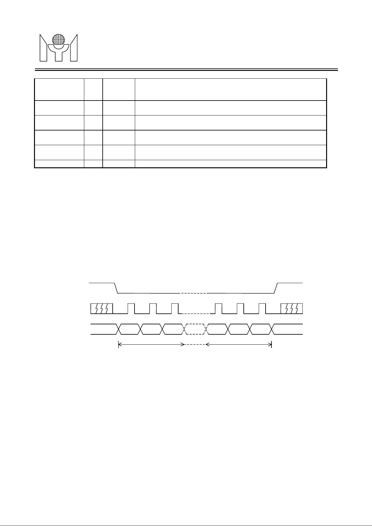
3.1.1 SPI bus
should start pulling SSB to "low" level, enabling MTV048 to receiving mode, and retain at "low" level
till the last cycle for a complete data packet transfer. The protocol is shown in Figure 1.
SSB
SCK
SDA
There are three transmission formats, shown as below:
Format (a) R - C - D → R - C - D → R - C - D …..
Format (b) R - C - D → C - D → C - D → C - D …..
Format (c) R - C - D → D → D → D → D → D …..
Where R=Row address, C=Column address, D=Display data
MSB LSB
First byte Last byte
FIGURE 1. Data Transm i s s i o n Prot o c ol (SPI)
3.1.2 I2C bus
2
I
the slave address 7AH to MTV048. The protocol is shown in Figure 2.
Rev 0.9 - 3 - 2001/03/15
Page 4
MYSON
Where S=Slave address, R=Row address, C=Column address, D=Display data
ab
c
ab
c
ab
c
There are 3 types of data, which should be accessed through the serial data interface. One is ADDRESS
bytes of display registers,
The bit6 of row address is used to distinguish display registers and user fonts RAM data
respectively. Bit5 of row address for display register is used to distinguish ADDRESS byte when it is set to
MTV048
TECHNOLOGY
(Rev 0.9)
SCK
SDA
START ACK
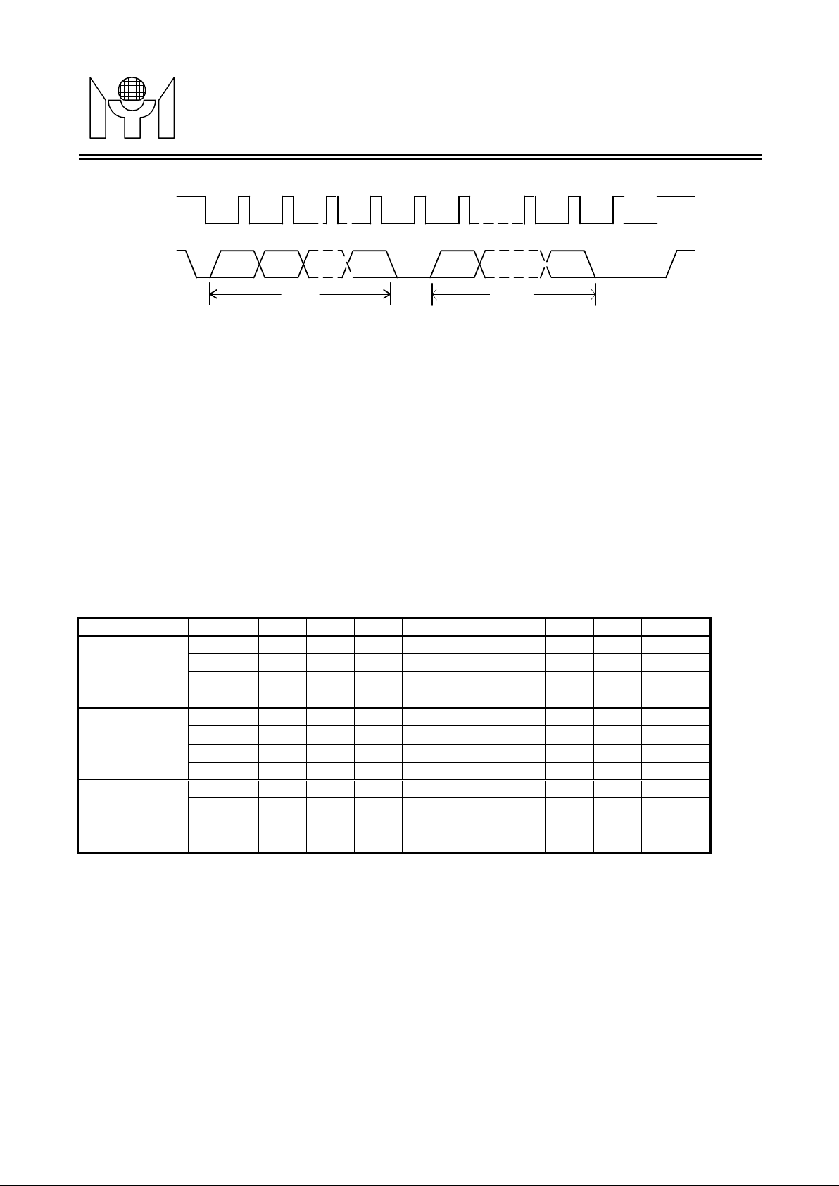
There are three transmission formats for I2C write mode, shown as below:
Format (a) S - R - C - D → R - C - D → R - C - D …..
Format (b) S - R - C - D → C - D → C - D → C - D …..
Format (c) S - R - C - D → D → D → D → D → D …..
Each arbitrary length of data packet consists of 3 portions viz, Row address (R), Column address (C), and
Display data (D). Format (a) is suitable for updating small amount of data, which will be allocat ed with a
different row address and column address. Format (b) is recommended for updating data that has the same
row address but a different column address. Massive data updating or full screen data chan ge should use
format (c) to increase transmission efficiency. The row and column address will be incremented
automatically when the format (c) is applied. Furthermore, the undefined locations in display or user fonts
RAM should be filled with dummy data.
B7 B6 B0 B7 B0
first byte
second byte last byte
FIGURE 2. Data Transm iss i o n Pro t o c o l (I2C)
ACK STOP
TABL E 1. The Configuration of Transmission Formats
Address b7 b6 b5 b4 b3 b2 b1 b0 Format
Row 1 0 0 R4 R3 R2 R1 R0 a,b,c
Address Bytes
of Disp lay Reg.
Attribu te Bytes
of Disp lay Reg.
User Fonts
bytes of display registers, another is ATTRIBUTE
RAM data. The protocols are all the same except the bit6 and bit5 of row address and the bit5 of column
address. The MSB (b7) is used to distinguish row and column addresses when transferring data from
external controller.
and the bit6 of column address is used to differentiate the column address for format (a), (b) and format (c)
"0" and ATTRIBUTE byte when it is set to "1". And at address bytes, bit5 of colum n address is the MSB
(bit8) and data bytes are the 8 LSB (bit7~bit0) of disp l ay fon t s address to save half MCU memory for
true 392 fonts display. So each one of the 384 fonts can be displayed at the same time. See Table 1. And for
format (c), since D8 is filled while program column address of address bytes, the continued d ata will be the
same bank of upper 128 fonts or lower 256 fonts until program column address is of address bytes again.
Column
Column
Data D7 D6 D5 D4 D3 D2 D1 D0 a,b,c
Row 1 0 1 R4 R3 R2 R1 R0 a,b,c
Column
Column
Data D7 D6 D5 D4 D3 D2 D1 D0 a,b,c
Row 1 1 - - - R2 R1 R0 a,b,c
Column
Column
Data D7 D6 D5 D4 D3 D2 D1 D0 a,b,c
0 0
0 1
0 0 x C4 C3 C2 C1 C0 a,b
0 1 x C4 C3 C2 C1 C0 c
0 0 C5 C4 C3 C2 C1 C0 a,b
0 1 C5 C4 C3 C2 C1 C0 c
D8
D8
C4 C3 C2 C1 C0 a,b
C4 C3 C2 C1 C0 c
and the other is user fonts
Rev 0.9 - 4 - 2001/03/15
Page 5
MYSON
3.2 Address Bus Admin ist rator
The external data write through serial data interface to registers must be synchronized by inter-
The vertical display control can generate different vertical display sizes for most display standards in current
( VERTD * 4 + 1 ) * H Where H = one horizontal line display time
MTV048
TECHNOLOGY
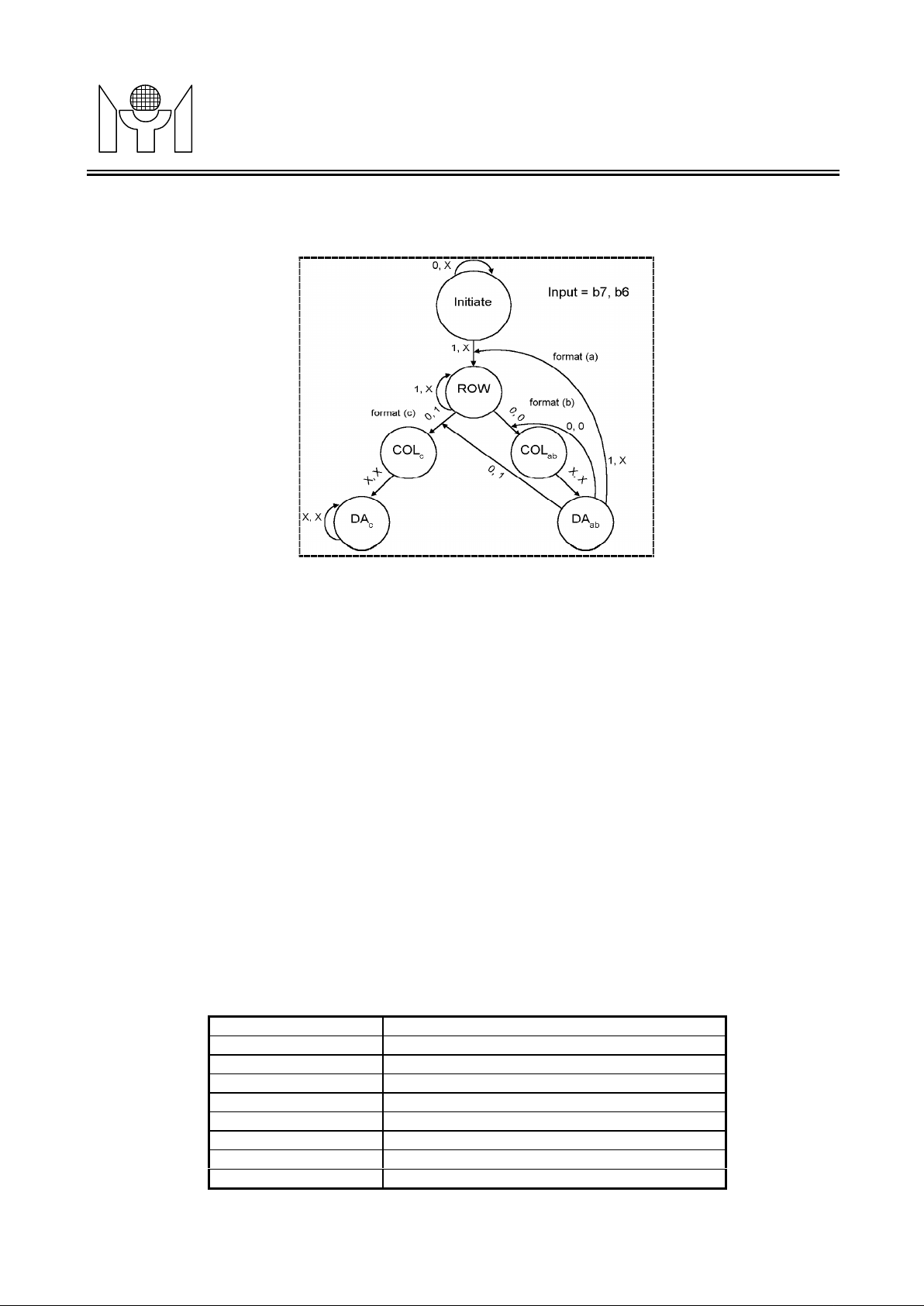
The data transmission is permitted to change from format (a) to format (b) and (c), or from format (b) to
format (a), but not from format (c) back to format (a) and (b). The alternation between transmission formats is
configured as the state diagram shown in Figure 3 .
FIGURE 3. Transmi s s i o n State Diagram
(Rev 0.9)
The administrator manages bus address arbitration of internal registers or user fonts RA M during external
data write in.
nal display timing. In addition, the administrator also provides automatic increment to address bus when
external write using format (c).
3.3 Vertical Display Cont ro l
monitors. The vertical display size is calculated with the information of double character he ight bit (CHS),
vertical display height control register (CH6-CH0). The algorithms of repeating character line display are
shown as Table 2 and Table 3. The range of programmable vertical size is 270 lines to 2130 lines maximum.
The vertical display center for full screen display could be figured out according to the information of vertical
starting position register (VERTD) and VFLB input. The vertical delay starting from the leading edge of VFLB
is calculated by using the following equation:
Vertical delay time =
TABLE 2. Repeat Line Weight of Character
CH6 – CH0 Repeat Line Weight
CH6, CH5 = 11 +18*3
CH6, CH5 = 10 +18*2
CH6, CH5 = 0x +18
CH4 = 1 +16
CH3 = 1 +8
CH2 = 1 +4
CH1 = 1 +2
CH0 = 1 +1
Rev 0.9 - 5 - 2001/03/15
Page 6
MYSON
The horizontal display control is used to generate control timing for horizontal display based on double char-
Where P = One XIN pixel dis
input is not present to MTV048, the PLL will generate a specific system clock, approximately 2.5MHz, by a
has its corresponding character address on ADDRESS byte
only even column characters could be displayed on screen and the odd colum n characters will be hidden.
MTV048
TECHNOLOGY
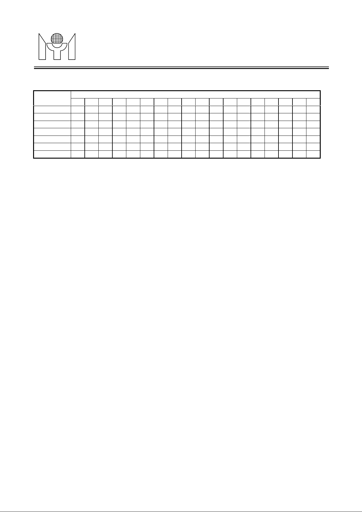
TABLE 3. Repeat Line Number of Character
Repeat Line #Repeat Lin e
Weight
+1 - - - - - - - - v - - - - - - - - +2 - - - - v - - - - - - - v - - - - +4 - - v - - - v - - - v - - - v - - +8 - v - v - v - v - v - v - v - v - -
+16 - v v v v v v v v v v v v v v v v +17 v v v v v v v v v v v v v v v v v +18 v v v v v v v v v v v v v v v v v v
Note: “v” means the nth line in the character would be repeated once, while “-“ means the nth line in the
character would not be repeated.
3.4 Horizont al Display Contro l
acter width bit (CWS), horizontal positioning register (HORD), horizontal resolution register (HORR), and
HFLB input. A horizontal display line consists of (HORR*12) dots which include 360 dots for 30 display characters and the remaining dots for blank region. The horizontal delay starting from HFLB leading edge is
calculated by using the following equation:
0 1 2 3 4 5 6 7 8 9 10 11 12 13 14 15 16 17
(Rev 0.9)
For CRT: Horizontal delay time = ( HORD * 6 + 49) * P - phase error detection pulse width
Where P = One pixel display time = One horizontal line display time / (HORR*12)
For LCD: Horizontal delay time = ( HORD * 6 + 49) * P
play time
3.5 Phase lock loo p (PLL)
On-chip PLL generates system clock timing (VCLK) by tracking the input HFLB and horizontal resolution register (HORR). The frequency of VCLK is determined by the following equation:
VCLK Freq. = HFLB Freq. * HORR * 12
The VCLK frequency ranges from 6MHz to 150MHz selected by (VCO1, VCO0). In addition, when HFLB
built-in oscillator to ensure data integrity.
3.6 Displ ay & Row Contro l Registers
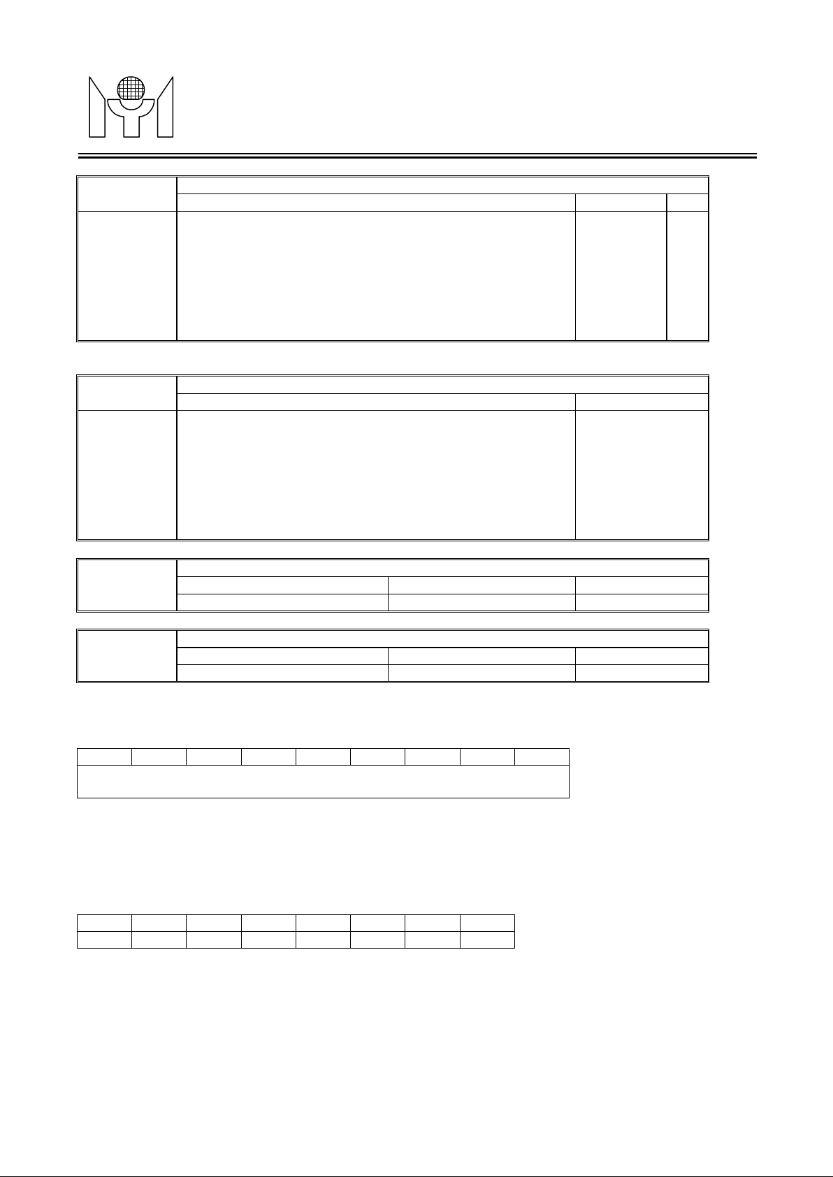
The internal RAM contains display and row control registers. The display registers ha ve 450 locations, which
are allocated between (row 0, column 0) to (row 14, column 29), as shown in Figure 4. Each display register
, its corresponding background color, 1 blink bit
and its corresponding color bits on ATTRIBUTE bytes. The row control register is allocated at column 30 for
row 0 to row 14, it is used to set character size to each respective row. If double width character is chosen,
Rev 0.9 - 6 - 2001/03/15
Page 7
MYSON
of Display Registers
of Display Registers
WINDOW1 ~ WINDOW4
WINDOW SHADOW COLOR
FIGURE 5. ATTRIBUTE Byt es of Dis p lay Registers Memor y Map
Row control registers (ROW 0 ~ 14, COLUMN 30),
CWS
Define double width character to the respective row. If double width character is chosen, only even
MTV048
Row #
Row #
TECHNOLOGY
Column #
0 1 28 29 30 31
0
1
Character ADDRESS Bytes
13
14
FIGURE 4. ADDRESS Byt es of Disp l ay Regis t er s Memo r y Map
0 1 28 29 30 31
0
1
13
14
Column #
Character ATTRIBUTE Bytes
ROW
CTRL REG
RESERVED
(Rev 0.9)
R
E
S
E
R
V
E
D
Column #
Row 15
Row 16
ADDRESS Byt es :
Address registers, (ROW 0 ~ 14, COLUMN 0 ~ 29),
B8 B7 B6 B5 B4 B3 B2 B1 B0
MSB LSB
CRADDR - Define OSD character address from address 0 to 383.
B7 B6 B5 B4 B3 B2 B1 B0
- - - BOX - - CHS
BOX - Select BGR, BGG, BGB or BOX2, BOX1, BOX0 of attributes bytes to the respective row.
= 0 ⇒ Background color bits BGR, BGG, BGB are selected.
= 1 ⇒ Button boxes bits BOX2, BOX1, BOX0 are selected.
0 11 12 22 23 31
FRAME CTRL REG. RESERVED
Column #
0 1 2 4 5 31
FRAME CTRL REG. RESERVED
CRADDR
= 0 ~ 359 ⇒ 360 standard ROM fonts.
= 360 ~ 367 ⇒ 8 user fonts.
= 368 ~ 383 ⇒ 16 multi-color ROM fonts.
CHS - Define double height character to the respective row.
CWS -
Rev 0.9 - 7 - 2001/03/15
Page 8

MYSON
There are 4 character button box generators to generate 4 different types of button boxes incl udi ng
defined by (BOX2, BOX1, BOX0) bits of attribute bytes. And these bits are described as below:
MTV048
TECHNOLOGY
column characters could be displayed on screen and the odd column characters will be hidden.
ATTRIBUTE Bytes:
Attribute registers, (ROW 0 ~ 14, COLUMN 0 ~ 29),
B7 B6 B5 B4 B3 B2 B1 B0
- BGR/BOX2 BGG/BOX1 BGB/BOX0 BLINK R G B
BGR, BGG, BGB : These three bits define the background color for their individual relative address
characters. If these three bits are set to (0, 0, 0), no background will be shown
(transparent). Therefore, a total of 7 background colors can be selected.
BOX2-0 - Select the character button boxes format of its relative address character.
= 0, 0, 0 ⇒ Button boxes is disabled.
= 1, 0, 0 ⇒ Start of depressed button box which is more than 1 character button box.
= 1, 0, 1 ⇒ Start of depressed button box which is only 1 character button box.
= 1, 1, 0 ⇒ Start of raised button box which is more than 1 character button box.
= 1, 1, 1 ⇒ Start of raised button box which is only 1 character button box.
= 0, 1, 0 ⇒ Middle of button box.
= 0, 0, 1 ⇒ End of button box.
BLINK = 1 ⇒ Enable blink effect for its relative address character. And the blinking is alternate per 32
vertical frames.
= 0 ⇒ Disable blink effect for its relative address character.
(Rev 0.9)
R, G, B - These three bits are used to specify their individual relative address character foreground color.
3.7 Character Butt o n Box es Generator
depressed button box with only 1 character, depressed button box with more than 1 character, raised button
box with only 1 character, and raised button box with more than 1 character. T he button boxes format is
1). (1, x, x) means the start of character button box, and than BOX1-0 bits define the format of button box.
2). (0, 1, 0) means the middle of character button box.
3). (0, 0, 1) means the end of character button box.
The length of button box is also software control by (BOX2, BOX1, BOX0) bits. For example, if there is 1
raised button box whose length is equal to 6 characters, these BOX2-0 bits will be (1, 1, 0), (0, 1, 0), (0, 1, 0),
(0, 1, 0), (0, 1, 0), (0, 0, 1). And if there is 1 depressed button box whose length is equal to 4 characters,
these BOX2-0 bits will be (1, 0, 0), (0, 1, 0), (0, 1, 0), (0, 0, 1). That is, (0, 1, 0) command's number defines
the button box length. And only 1 byte, the attribute byte of button box start character, shou ld be modified
when changing button box type from raised button to depressed button, or vice versa. This is very easy and
useful for software programming.
3.8 Character ROM
MTV048 character ROM contains 384 characters and symbols including 360 standard fonts, 8 user fonts and
16 multi-color fonts. The 360 standard fonts are located from address 0 to 359. The 8 user fonts are located
from address 360 to 367.And the 16 multi-color fonts are located from address 368 to 383. Each character
and symbol consists of 12x18 dots matrix.
Rev 0.9 - 8 - 2001/03/15
Page 9

MYSON
BOX2-0 = 1, 0, 1 1, 0, 0 0, 0, 1 1, 0, 0 0, 1, 0 0, 1, 0 0, 0, 1
MTV048
TECHNOLOGY
B2~B0 = 1, 1, 1 1, 1, 0 0, 0, 1 1, 1, 0 0, 1, 0 0, 1, 0 0, 0, 1
(Rev 0.9)
Depressed Button Boxes
FIGURE 6. Character Bu t t o n Boxes
3.9 Multi -Color Font
The color fonts comprise three different R, G, B fonts. When the code of color font is accessed, the separate
R/G/B dot pattern is output to corresponding R/G/B outputs. See Figure 7 for the sample displayed color font.
Note: No black color can defined in color font, black window underline the color font can make the dots
become black in color.
B
G
R
Magenta
Green
Blue
Cyan
FIGURE 7. Example of Mul t i -co l o r Font
Rev 0.9 - 9 - 2001/03/15
Page 10
MYSON
bytes data,
FIGURE 6. User Fon ts RAM Memo ry Map
Column# Data Colum n# Data
MTV048
TECHNOLOGY
(Rev 0.9)
TABL E 4. The Multi-color Font Color Selection
R G B
Background Color 0 0 0
Blue 0 0 1
Green 0 1 0
Cyan 0 1 1
Red 1 0 0
Magenta 1 0 1
Yellow 1 1 0
White 1 1 1
3.10 User fo n ts RAM
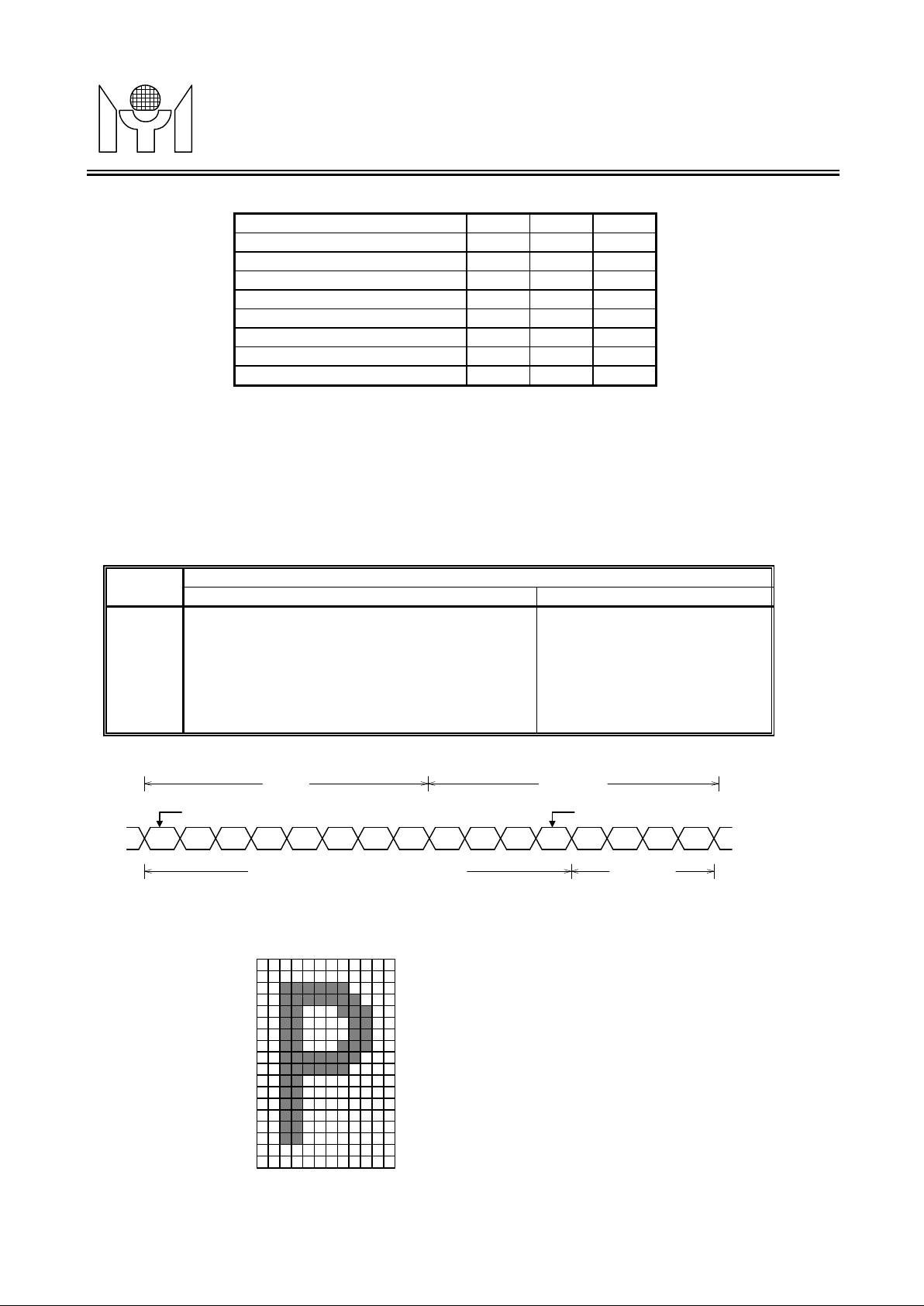
The user fonts RAM have 288 locations, which are allocated between (row 0, column 0) to (row 7, column 35)
to specify 8 user programmable fonts, as shown in Figure 6. Each user programmable font consists of 12x18
dot matrix which data are stored in 36 bytes registers. And each line of dot matrix consists of 2
which include 4 dummy bits as shown in figure 7 and figure 8. For example, font 0 is stored in row 0 from
column 0 to column 35 and font 1 is stored in row 1 from colum n 0 to column 35, etc.
ROW # COLUMN #
0 1 34 35 36 63
0
1
6
7
b7 b6 b5 b4 b3 b2 b1 b0 b7 b6 b5 b4 b3 b2 b1 b0
Where N=even number
Nth byte (N+1)th byte
leftmost dot of font
12 bits for one row data of font dot matrix Dummy bits
USER FONTS RAM RESERVED
rightmost dot of font
FIGURE 7. Data Form at of User Font Dot Matr i x
0 00H 1 00H
2 00H 3 00H
4 3FH 5 00H
6 3FH 7 80H
8 31H 9 C0H
10 30H 11 C0H
12 30H 13 C0H
14 31H 15 C0H
16 3FH 17 80H
18 3FH 19 00H
20 30H 21 00H
22 30H 23 00H
24 30H 25 00H
26 30H 27 00H
28 30H 29 00H
30 30H 31 00H
32 00H 33 00H
34 00H 35 00H
FIGURE 8. Exampl e of User Font Prog r amm i n g
Rev 0.9 - 10 - 2001/03/15
Page 11
MYSON
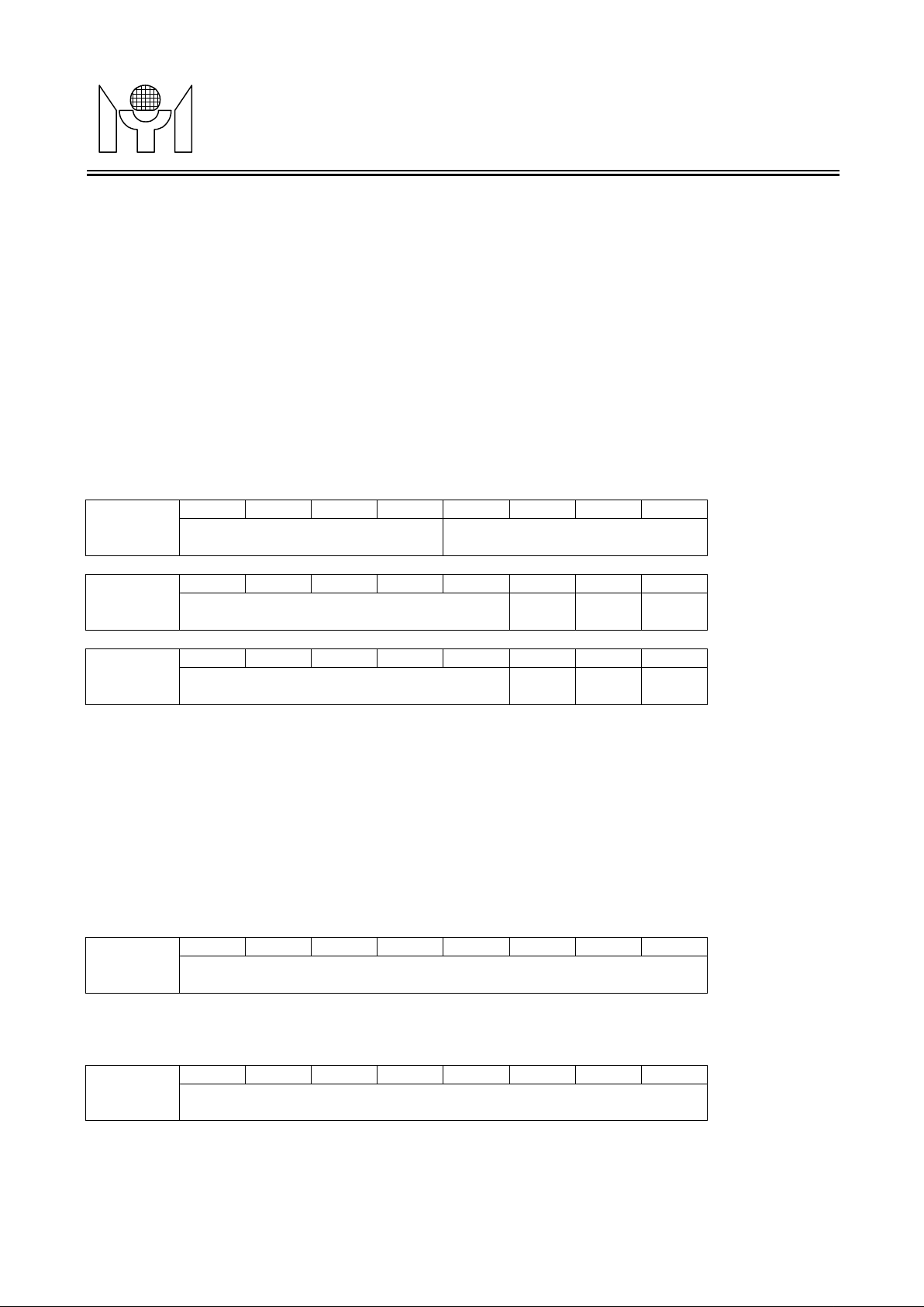
1. Window control registers,
ROW START ADDR
ROW END ADDR
WSHD
VERTD - Specify the starting position for vertical display. The total steps are 256, and the increment of each
step is 4 Horizontal display lines. The initial value is 4 after power up.
HORD - Define the starting position for horizontal display. The total steps are 256, and the increment of each
MTV048
TECHNOLOGY
3.11 Lumi n ance & Bor d er Generator
There are 3 shift registers included in the design which can shift out of luminance and border dots to color
encoder. The bordering and shadowing feature is configured in this block. For bordering effect, the character
will be enveloped with blackedge on four sides. For shadowing effect, the character is envelo ped with
blackedge for right and bottom sides only.
3.12 Windo w and Frame Cont r o l
The display frame position is completely controlled by the contents of VERTD and HORD. The window size
and position control are specified in column 0 to 11 on row 15 of memory map, as shown in Figure 5.
Window 1 has the highest priority, and window 4 is the least, when two windows are overlapping. More
detailed information is described as follows:
ROW 15
Column
0,3,6 or 9
Column
1,4,7 or 10
b7 b6 b5 b4 b3 b2 b1 b0
MSB LSB
b7 b6 b5 b4 b3 b2 b1 b0
COLUMN START ADDR
MSB LSB
MSB LSB
WEN -
(Rev 0.9)
Column
2,5,8 or 11
START(END) ADDR - These addresses are used to specify the windo w size. It should be noted that when
WEN - Enable the relative background window display.
WSHD - Enable shadowing on the relative window.
R, G, B - Specify the color of the relative background window.
2. Frame control registers,
ROW 15
Colum n 12
Colum n 13
b7 b6 b5 b4 b3 b2 b1 b0
COLUMN END ADDR
MSB LSB
the start address is greater than the end address, the window would be disabled.
b7 b6 b5 b4 b3 b2 b1 b0
VERTD
MSB LSB
b7 b6 b5 b4 b3 b2 b1 b0
HORD
MSB LSB
R G B
Rev 0.9 - 11 - 2001/03/15
step is 6 dots. The initial value is 15 after power up.
Page 12
MYSON
be appended below each display row, and the maximum space is 31 lines. The initial va lue is 0
SHADOW
WINCLR
second to fully display the whole menu or to disappear completely.
playing of characters or windows, otherwise, it outputs high only during the displaying of
MTV048
TECHNOLOGY
Colum n 14
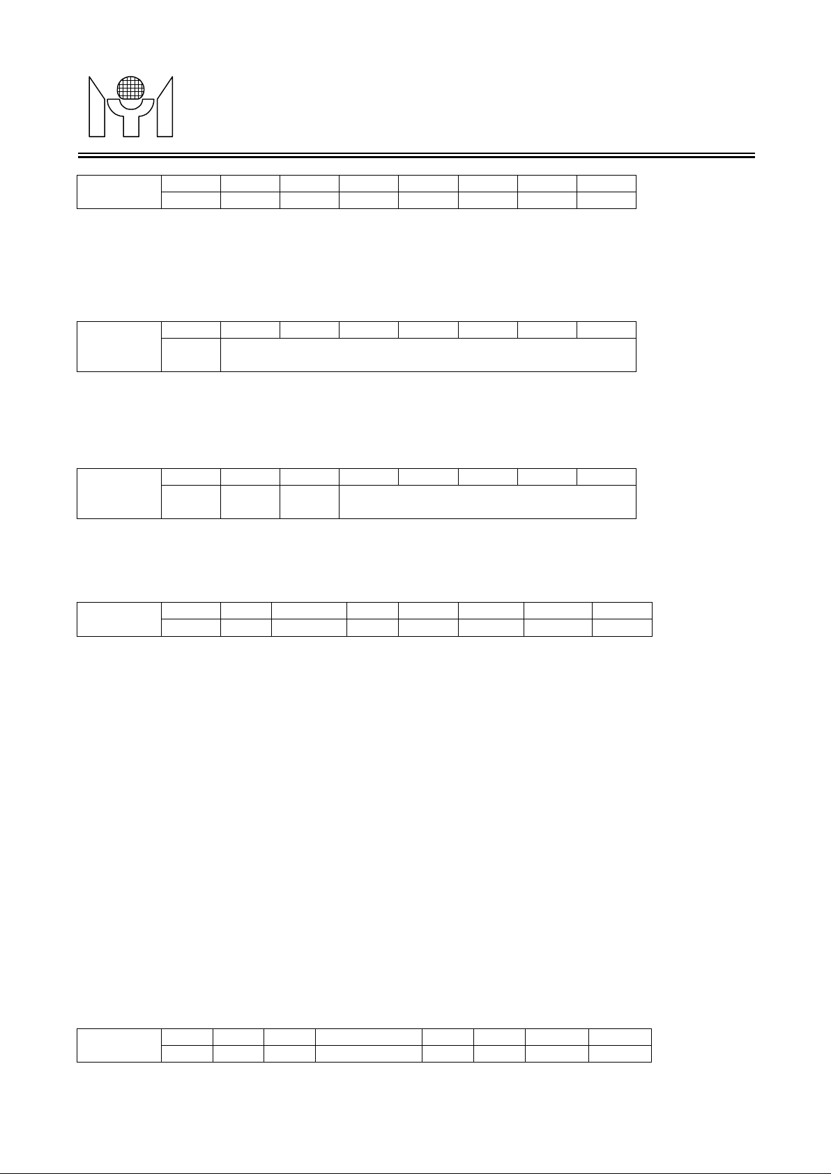
CH6-CH0 - Define the character vertical height, the height is programmable from 18 to 71 lines. The
Colum n 15
(This byte is used only for CRT monitor application.)
HORR - Specify the resolution of a horizontal display line, and the increment of each step is 12 dots. That is,
the pixels' number per H line equal to HORR*12. It is recommended that HORR should be greater
than or equal to 36 and smaller than 150M / (Hfreq*12). The initial value is 40 after po wer up.
Colum n 16
b7 b6 b5 b4 b3 b2 b1 b0
- CH6 CH5 CH4 CH3 CH2 CH1 CH0
character vertical height is at least 18 lines if the content of CH6-CH0 is less than 18. For
example, when the content is " 2 ", the character vertical height is regarded as equal to 20 lines.
And if the content of CH4-CH0 is greater than or equal to 18, it will be regarded as equal to 17.
See Table 2 and Table 3 for detail description of this operation.
b7 b6 b5 b4 b3 b2 b1 b0
- HORR
MSB LSB
b7 b6 b5 b4 b3 b2 b1 b0
- - - RSPACE
MSB LSB
(Rev 0.9)
RSPACE - Define the row to row spacing in unit of horizontal line. That is, extra RSPAC E h orizontal lines will
after power up.
Colum n 17
OSDEN - Activate the OSD operation when this bit is set to "1". The initial value is 0 after power up.
BSEN - Enable the bordering and shadowing effect.
SHADOW - Activate the shadowing effect if this bit is set, otherwise the bordering is chosen.
FBEN - Enable the fade-in/fade-out or blend-in/blend-out effect when OSD is turned on from off state or vice
versa.
BLEND - Fade-in/fade-out or blend-in/blend-out effect select bit. Activate the blend-in/blend-out effect if this
bit is set, otherwise the fade-in/fade-out function is chosen. This function roughl y takes about 0.5
WENCLR - Clear all WEN bits of window control registers when this bit is set to "1". The initial value is 0 after
RAMCLR - Clear all ADDRESS bytes, BGR, BGG, BGB and BLINK bits of display registers when this bit is
b7 b6 b5 b4 b3 b2 b1 b0
OSDEN BSEN
power up.
set to "1". The initial value is 0 after power up.
FBEN BLEND
RAMCLR FBKGC
FBKGC - Define the output configuration for FBKG pin. When it is set to "0", the FBKG outputs high during
the dis
character.
Colum n 18
Rev 0.9 - 12 - 2001/03/15
b7 b6 b5 b4 b3 b2 b1 b0
TRIC FSS - SELVCL/DWE HSP VSP VCO1/- VCO0/-
Page 13
MYSON
(DWE bit is used only for LCD monitor applications.)
Accept negative polarity Hsync input.
Accept positive polarity Vsync input.
Accept negative polarity Vsync input.
MTV048
TECHNOLOGY
(SELVCL, VCO1, VCO0 bits are used for CRT monitor applications only.)
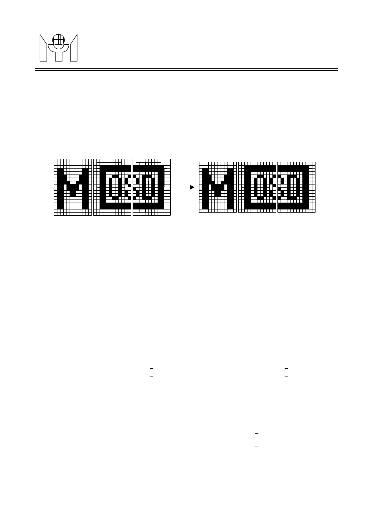
TRIC - Define the driving state of output pins ROUT, GOUT, BOUT and FBKG when OSD is disabled. That
is, while OSD is disabled, these four pins will drive low if this bit is set to 1, otherwise these four pins
are in high impedance state. The initial value is 0 after power up.
FSS - Font size selection.
= 1 ⇒ 12x18 font size is selected.
= 0 ⇒ 12x16 font size is selected.
Fonts desig n ed to be 12x18 display 12x16 display if FSS=0; first and last li n es omit t ed
FIGURE 8. 12x18 and 12x16 Fonts
(Rev 0.9)
SELVCL - Enable auto detection for horizontal and vertical syncs input edge distortion to avo id unstable
Vsync leading mismatch with Hsync signal while the bit is set to "1". The initial value is 0 after
power up.
HSP - = 1 ⇒ Accept positive polarity Hsync input.
= 0 ⇒
VSP - = 1 ⇒
VCO1, VCO0 - Select the appropriate curve partitions of VCO frequency to voltage based on HFLB input
(i) 5.6K ohm: (ii) 3.3K ohm:
= (0, 0) ⇒ 6MHz < Pixel rate < 24MHz = (0, 0) ⇒ 6MHz < Pixel rate < 28MHz
= (0, 1) ⇒ 24MHz < Pixel rate < 48MHz = (0, 1) ⇒ 28MHz < Pixel rate < 56MHz
= (1, 0) ⇒ 48MHz < Pixel rate < 96MHz = (1, 0) ⇒ 56MHz < Pixel rate < 112MHz
= (1, 1) ⇒ 96MHz < Pixel rate < 128MHz = (1, 1) ⇒ 112MHz < Pixel rate < 150MHz
Notes:
1. That is, if HORR is specified and RP resister = 3.3K ohm, then (VCO1, VCO0)
2. It is necessary to wait for the PLL to become stable while (i) the HORR register is changed; (ii) the (VCO1, VCO0)
3. When PLL is unstable, do not write data in any address except Column 15,17,18 of Row 15. If data is written in
= 0 ⇒
and horizontal resolution register (HORR). And there are different curve partitions based on
different application resister value on pin 3 (pin RP) as below:
Where Pixel rate = VCLK Freq = HFLB Freq * HORR * 12
The initial value is (0, 0) after power up.
= (0, 0), if 6000/(HORR * 12) < HFLB Freq (KHz) < 28000/(HORR * 12)
= (0, 1), if 28000/(HORR * 12) < HFLB Freq (KHZ) < 56000/(HORR * 12)
= (1, 0), if 56000/(HORR * 12) < HFLB Freq (KHZ) < 112000/(HORR * 12)
= (1, 1), if 112000/(HORR * 12) < HFLB Freq (KHZ) < 150000/(HORR * 12)
bits is changed; (iii) the horizontal signal (HFLB) is changed.
any other address, a malfunction may occur.
Rev 0.9 - 13 - 2001/03/15
Page 14
MYSON
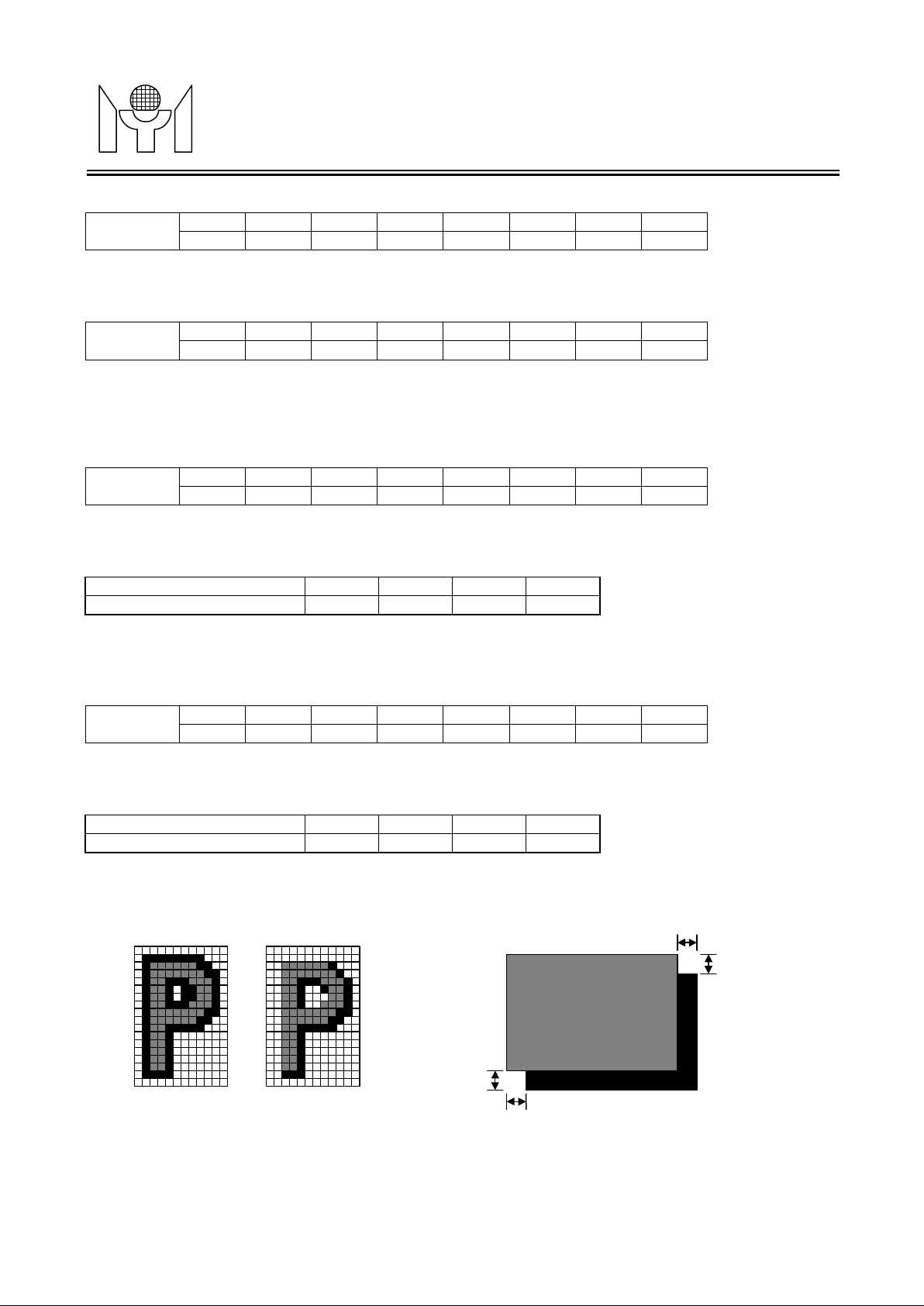
FSW - Enable full screen self-test pattern and force the FBKG pin output to high to disable video RGB while
WW41
WW40
WW31
WW30
WW21
WW20
WW11
WW10
WH41
WH40
WH31
WH30
WH21
WH20
WH11
WH10
Determine the shadow height of window 4 when WSHD bit of window 4 is enable d.
Determine the shadow height of window 3 when WSHD bit of window 3 is enable d.
Determine the shadow height of window 2 when WSHD bit of window 2 is enable d.
Determine the shadow height of window 1 when WSH
Note:
N Horizontal lines
N Horizontal lines
MTV048
TECHNOLOGY
Colum n 19
CSR, CSG, CSB - Define the color of bordering or shadowing on characters. The initia l value is (0, 0, 0) after
Colum n 20
FSR, FSG, FSB - Define the color of full screen self-test pattern.
Colum n 21
WW41, WW40 - Determine the shadow width of window 4 when WSHD bit of window 4 is enabled.
(WW41, WW40) (0, 0) (0, 1) (1, 0) (1, 1)
Shadow Width (unit in Pixel) 2 4 6 8
b7 b6 b5 b4 b3 b2 b1 b0
- - - - - CSR CSG CSB
power up.
b7 b6 b5 b4 b3 b2 b1 b0
FSW - - - - FSR FSG FSB
this bit is set to "1". The self-test pattern's color is determined by (FSR, FSG, FSB) bits.
b7 b6 b5 b4 b3 b2 b1 b0
Please refer to the table below for more details.
(Rev 0.9)
WW31, WW30 - Determine the shadow width of window 3 when WSHD bit of window 3 is enabled.
WW21, WW20 - Determine the shadow width of window 2 when WSHD bit of window 2 is enabled.
WW11, WW10 - Determine the shadow width of window 1 when WSHD bit of window 1 is enabled.
Colum n 22
WH41, WH40 -
(WH41, WH40) (0, 0) (0, 1) (1, 0) (1, 1)
Shadow Height (unit in Line) 2 4 6 8
WH31, WH30 WH21, WH20 WH11, WH10 -
Bordering Shadowing
b7 b6 b5 b4 b3 b2 b1 b0
Please refer to the table below for more details.
D bit of window 1 is enabled.
M Pixels
M and N are defin ed
by the registers of
WINSW and WINSH.
M Pixels
FIGURE 9. Character Bord ering and Shadowing and Shadowing on Window
Rev 0.9 - 14 - 2001/03/15
Page 15
MYSON
- These 4 bits define the propagation delay of Rout, Gout, Bout, FBKG and INT outputs to pin XIN
MTV048
TECHNOLOGY
3.13 Color Encoder
The decoder generates the video output to ROUT, GOUT and BOUT by integrating window color, border
blackedge, luminance output and color selection output (R, G, B) to form the desired video outputs.
Column 23 ~ colu mn 31 : Reserved.
Note : The regist er loc ated at column 31 of row 15 is reserved for th e testing . Do not pro g ram thi s
byte anytime in normal operation.
ROW 16
Column 0
R1, G1, B1 - Define the shadow color of window 1. The initial value is (0, 0, 0) after power up.
R2, G2, B2 - Define the shadow color of window 2. The initial value is (0, 0, 0) after power up.
Column 1
b7 b6 b5 b4 b3 b2 b1 b0
- R1 G1 B1 - R2 G2 B2
b7 b6 b5 b4 b3 b2 b1 b0
- R3 G3 B3 - R4 G4 B4
(Rev 0.9)
R3, G3, B3 - Define the shadow color of window 3. The initial value is (0, 0, 0) after power up.
R4, G4, B4 - Define the shadow color of window 4. The initial value is (0, 0, 0) after power up.
Column 2
(This byte is used only for LCD monitor application.)
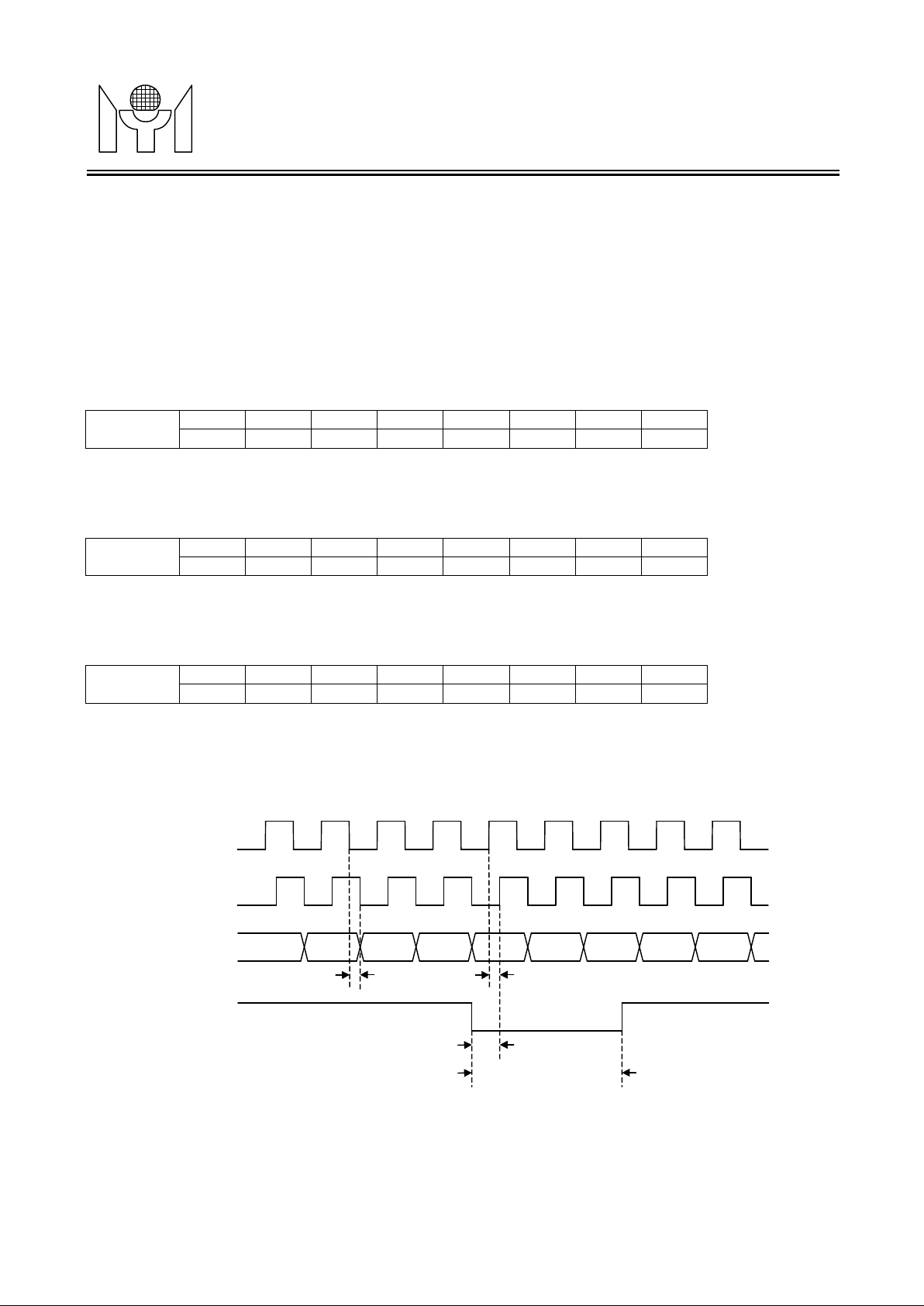
D3-D0
input falling edge control registers. Please refer to Figure 12 and Table 8.
OSD output
b7 b6 b5 b4 b3 b2 b1 b0
- - - - - D2 D1 D0
tPD
tPD
tSETUP
tHOLD
FIGURE 12. Outpu t and HFLB Timi n g to Pixel Clo ck
Rev 0.9 - 15 - 2001/03/15
Page 16

MYSON
default value except this byte. So this bit
MTV048
TECHNOLOGY
TABLE 7. Outpu t Timin g to Pixel Cloc k
Symbol (D2, D1, D0) Min. Typ. Max. Unit
tpd
Column 3 : Reserved.
Column 4
LCD - OSD application selection.
= 1 ⇒ LCD monitor application selected. The 2nd and 3rd pins are XIN, NC.
= 0 ⇒ CRT monitor application selected. The 2nd and 3rd pins are VCO, RP.
After this bit is changed, the whole chip circuit will be reset to
also can work as software reset bit. The initial value is 0 after power up.
b7 b6 b5 b4 b3 b2 b1 b0
LCD - ID5 ID4 ID3 ID2 ID1 ID0
(Rev 0.9)
0
1
2
3
4
5
6
7
-
-
-
-
-
-
-
-
TBD
TBD
TBD
TBD
TBD
TBD
TBD
TBD
-
-
-
-
-
-
-
-
ns
ns
ns
ns
ns
ns
ns
ns
ID5-ID0 - LCD bit identify bits. LCD bit can be updated to "1" only when ID5-ID0 = (0, 1, 0, 1, 0, 1). And LCD
bit can be updated to "0" only when ID5-ID0 = (1, 0, 1, 0, 1, 0).
Column 6 ~ colu mn 31 : Reserved.
Rev 0.9 - 16 - 2001/03/15
Page 17
MYSON
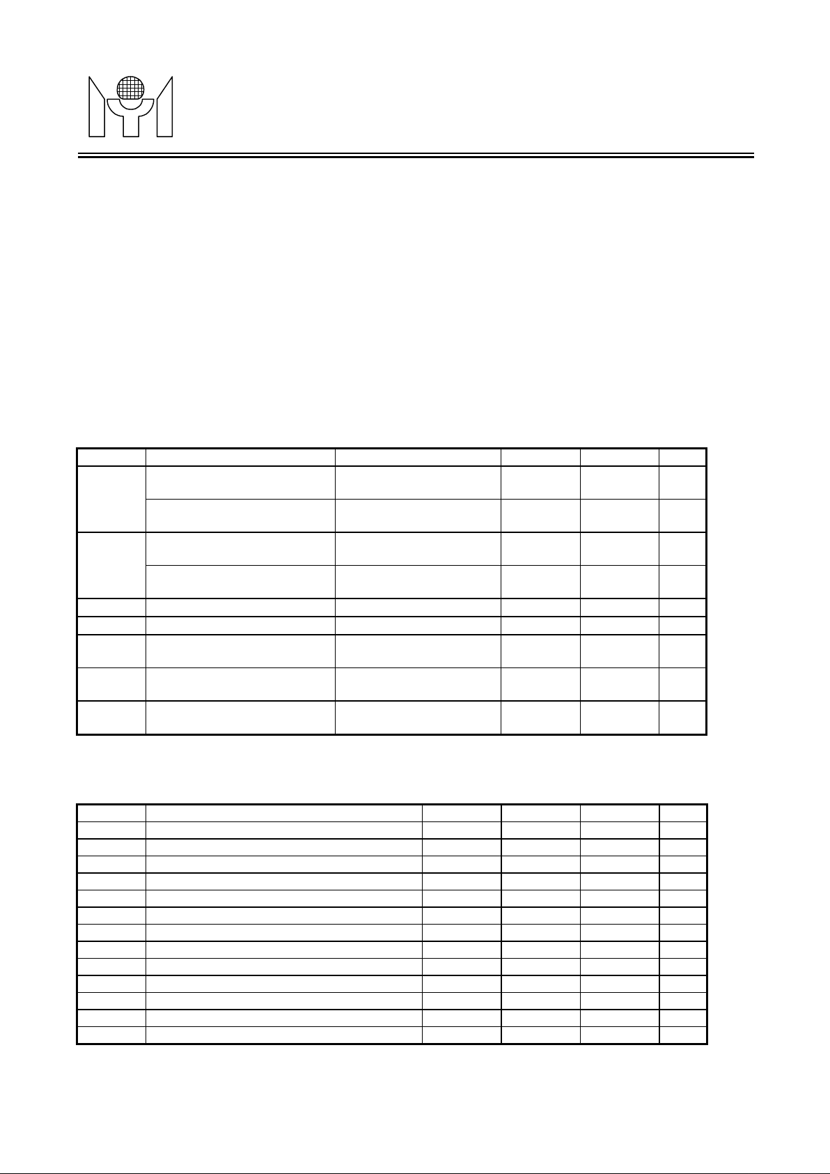
4.0 ABSOLUTE MAXIMUM RATINGS
6.0 ELECTRICAL CHARACTERISTICS (Under Operat in g Con di t io n s)
Standby Current
7.0 SWITCHING CHARACTERISTIC (Under Oper at in g Condi ti on s)
MTV048
TECHNOLOGY
(Rev 0.9)
DC Supply Voltage (VDD,VDDA) -0.3 to +7 V
Voltage with respect to Ground -0.3 to VDD+0.3 V
Storage Temperature -65 to +150 oC
Ambient Operating Temperature 0 to +70 oC
5.0 OPERATING CONDITIONS
DC Supply Voltage (VDD,VDDA) +4.75 to +5.25 V
Operating Temperature 0 to +70 oC
SYMBOL PA RA METER CONDITIONS (NOTES) MIN. MAX. UNITS
Input High Voltage
V
IH
(pin hflb, vflb, sda, sck)
Input High Voltage
(pin ssb)
Input Low Voltage
V
IL
(pin hflb, vflb, sda, sck)
Input Low Voltage
(pin ssb)
V
OH
V
OL
V
ODL
I
CC
I
SB
Output High Voltage
Output Low Voltage
Open Drain Output Low
Voltage
Operating Current
Pixel rate=96MHz
- 0.6 * VDD VDD+0.3 V
0.7 * VDD VDD+0.3 V
-
-
I
≥ -5 mA
OH
IOL≤ 5 mA
5 mA ≥ I
I
load
ODL
= 0uA
Vin = VDD,
I
= 0uA
load
VSS-0.3 0.25 * VDD V
VSS-0.3 0.2 * VDD V
VDD-0.8 - V
- 0.5 V
- 0.5 V
- 25 mA
- 12 mA
SYMBOL PARAMETER MIN. TYP. M AX. UNITS
f
HFLB
T
T
t
BCSU
t
BCH
t
DCSU
t
DCH
t
SCKH
t
SCKL
t
SU:STA
t
HD:STA
t
SU:STO
t
HD:STO
r
f
HFLB input frequency 15 - 150 KHz
Output rise time - - 5 ns
Output fall time - - 5 ns
SSB to SCK set up time 200 - - ns
SSB to SCK hold time 100 - - ns
SDA to SCK set up time 200 - - ns
SDA to SCK hold time 100 - - ns
SCK high time 500 - - ns
SCK low time 500 - - ns
START condition setup time 500 - - ns
START condition hold time 500 - - ns
STOP condition setup time 500 - - ns
STOP condition hold time 500 - - ns
Rev 0.9 - 17 - 2001/03/15
Page 18
MYSON
SCK
SDA
MTV048
TECHNOLOGY
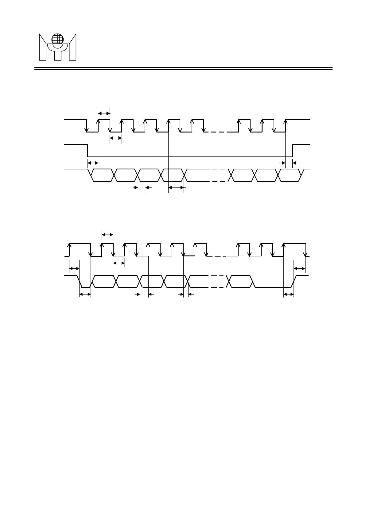
8.0 TIMING DIAGRAMS
SCK
SSB
t
BCSU
SDA
t
SCKH
t
SCKL
t
DCSU
t
DCH
FIGURE 11. Data Inter face Timing (SPI)
t
SCKH
(Rev 0.9)
t
BCH
t
SU:STA
t
HD:STA
t
SCKL
t
DCSU
t
DCH
FIGURE 12. Data Interface Timin g (I2C)
t
SU:STO
t
HD:STO
Rev 0.9 - 18 - 2001/03/15
Page 19
MYSON
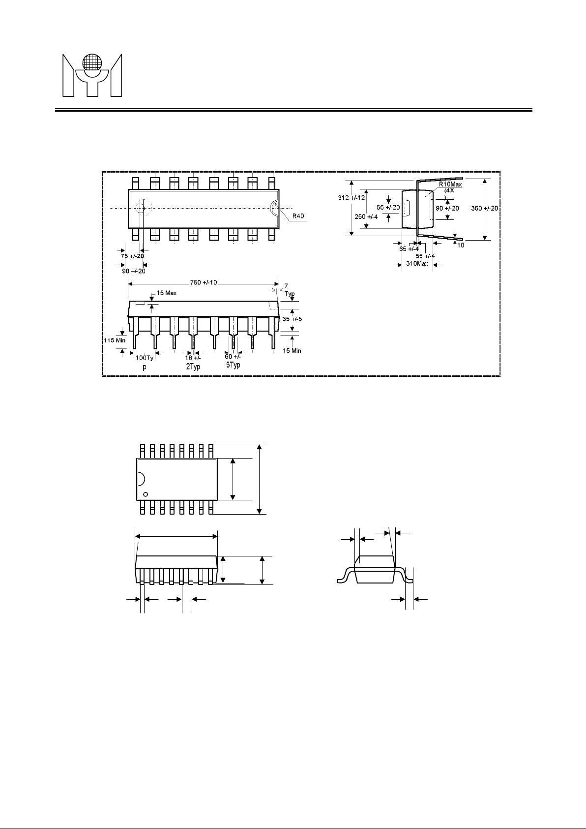
9.0 PACKAGE DIMENSION
0.406 +/-0.013
0.295 +/-0.004
0.406 +/-0.008
0.091
0.098 +/-0.006
0.016 +/-0.004
0.0501
(4x)
0.028 +0.022 /-0.013
0.015x45°
7°(4x)
MTV048
TECHNOLOGY
9.1 16 Pin PDIP 300mil
(Rev 0.9)
9.2 16 Pin SOP 300mil
Rev 0.9 - 19 - 2001/03/15
 Loading...