

Page 1
MYSON
MTV003N
TECHNOLOGY
(MTV003)
Microprocessor Compatible Monitor Controller
FEATURES
• Synchronous signal processing for use in green monitor applications.
• Easy command interface for external microprocessor controls.
• D/A converters up to 12V output.
• Built-in self-test pattern generator.
• On-chip clock oscillator allows external TTL level clock signal input.
GENERAL DESCRIPTION
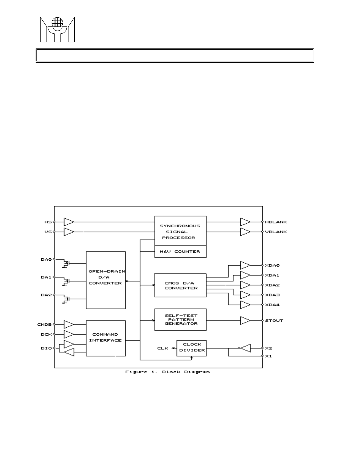
MTV003 is intended for use in digital-controlled, power-conscious (Green) monitor applications. It integrates 4
major function blocks traditionally implemented in discrete parts and provides an easy interface for
microprocessor controls. The functional blocks included in MTV003 are: SYNC processing, D/A converters,
self-test pattern generator and command interface.
BLOCK DIAGRAM
This datasheet contains new product information. Myson Technology reserves the rights to modify the product specification without notice.
No liability is assumed as a result of the use of this product. No rights under any patent accompany the sale of the product.
1/13
MTV003 Revision 2.3 07/01/1998
Page 2

MYSON
MTV003N
TECHNOLOGY
1.0 CONNECTION DIAGRAM
(20 PIN PDIP 300 MIL PACKAGE)
(MTV003)
2.0 PIN DESCRIPTIONS
Name I/O Pin# Function
VSS 1
DA0 O 2
DA1 O 3
DA2 O 4
HBLANK O 5
VBLANK O 6
X1 I/O 7
Ground (0 V).
Open-Drain PWM (Pulse Width Modulation) D/A Converter 0. The
output pulse width is programmable by writing data to Reg10 with
8-bit resolution to control the pulse width duration from 0 to 255/256.
The output frequency is 31.25KHz (or15.625KHz). In applications, the
external pull-up resistor can be connected to 12V for the desired fullscale output.
Open-Drain PWM D/A Converter 1. See DA0. The output pulse
width is programmable by Reg11.
Open-Drain PWM D/A Converter 2. See DA0. The output pulse
width is programmable by Reg12.
Horizontal Blank. The pulse width and the delay of HBLANK vs.HS
input leading edges are programmable by Reg7 and Reg6,
respectively.
Vertical Blank. The output pulse width is programmable by Reg9.
Crystal 1. Used to interface to the oscillator. An 8MHz(or 4MHz)
crystal must be connected between this pin and pin X2. An appropriate
capacitor to Ground, whose value depends on the specified CLof the
crystal, must be connected. This pin can also be used as a direct input
when the external oscillator is used.
MTV003 Revision 2.3 07/01/1998
2/13
Page 3

MYSON
MTV003N
TECHNOLOGY
Name I/O Pin# Function
X2 O 8
HS I 9
VS I 10
CMDB I 11
DCK I 12
DIO I/O 13
STOUT O 14
XDA4 O 15
XDA3 O 16
XDA2 O 17
XDA1 O 18
XDA0 O 19
VDD 20
Crystal 2. See X1. An appropriate capacitor to Ground, whose value
depends on the specified CLof the crystal, must be connected. For the
external clock source, this pin must be tied to Ground.
Horizontal Sync. Horizontal synchronous signal input. The input level
is TTL compatible with internal 0.2V hysteresis. An internal 50K Ohm
pull-up resistor is connected to this pin.
Vertical Sync. Vertical synchronous signal input. The input level is
TTL compatible with internal 0.2V hysteresis. An internal 50K Ohm
pull-up resistor is connected to this pin.
Command Interface Enabler. A low active pin which must be forced
to low in excess of 1 6 cycles of DCK for 1 successful access of
command interface. It has an internal 50K Ohm pull-up resistor.
Command Interface Clock. This pin is used as the timing base for
command interface. The address or data portion for the serial in (out)
of DIO is recognized by counting the number of DCKs. It has an
internal 50K Ohm pull-up resistor.
Command Interface Data. This pin is a bidirectional pin. A
microprocessor can access any internal command registers through
the protocol of the address portion followed by the succeeding data
portion. It must complete 16 full DCK cycles for a valid access.
Self-Test Video Output. (for self-test mode) This pin is the video
output pin of the self-test pattern generator. The generator enabler,
pattern modes, output band selection and output enabler are
programmed by Reg16.
CMOS PWM D/A Converter 4. See DA0. The output pulse width can
be programmed by Reg30. It is a CMOS type output.
CMOS PWM D/A Converter 3. See DA0. The output pulse width can
be programmed by Reg29. It is a CMOS type output.
CMOS PWM D/A Converter 2. See DA0. The output pulse width can
be programmed by Reg28. It is a CMOS type output.
CMOS PWM D/A Converter 1. See DA0. The output pulse width can
be programmed by Reg27. It is a CMOS type output.
CMOS PWM D/A Converter 0. See DA0. The output pulse width can
be programmed by Reg26. It is a CMOS type output.
Positive Power Supply. +5 volts. 2 decoupling capacitors, 0.1 uF and
100 uF, must be connected to VDD and Ground as close to the device
as possible.
(MTV003)
3.0 FUNCTIONAL DESCRIPTION
3.1 Crystal Oscillator and Clock Generator
The crystal oscillator shall be connected to an 8MHz(or 4MHz) crystal. X1, as shown in Fig.1, can be used as
an input source for the external clock or an output clock source to drive the external MCU. All timing
specifications are based on the frequency of X1 (or X1 divided by 2).
3.2 PWM D/A Converter
There are 2 types of D/A converters with 8-bit resolution: open-drain type (DA0 to DA2) and CMOS type (XDA0
to XDA4). The sampling frequency is 31.25KHz or 15.625KHz, depending on the use of the crystal. The
maximum external voltage applied is 12V for the open-drain type, and the output pulse width is programmable
MTV003 Revision 2.3 07/01/1998
3/13
Page 4
MYSON
MTV003N
TECHNOLOGY
for each converter by setting the corresponding register.
3.3 SYNC Processor
The sync processor contains the following functions: polarity detection, presence detection, H-Freq counter,
V-Freq counter and sync signal separation for input SYNC sources (HS and VS). It can be programmed to
change the detected polarity status and output polarity of SYNC pins (HBLANK and VBLANK) by using the
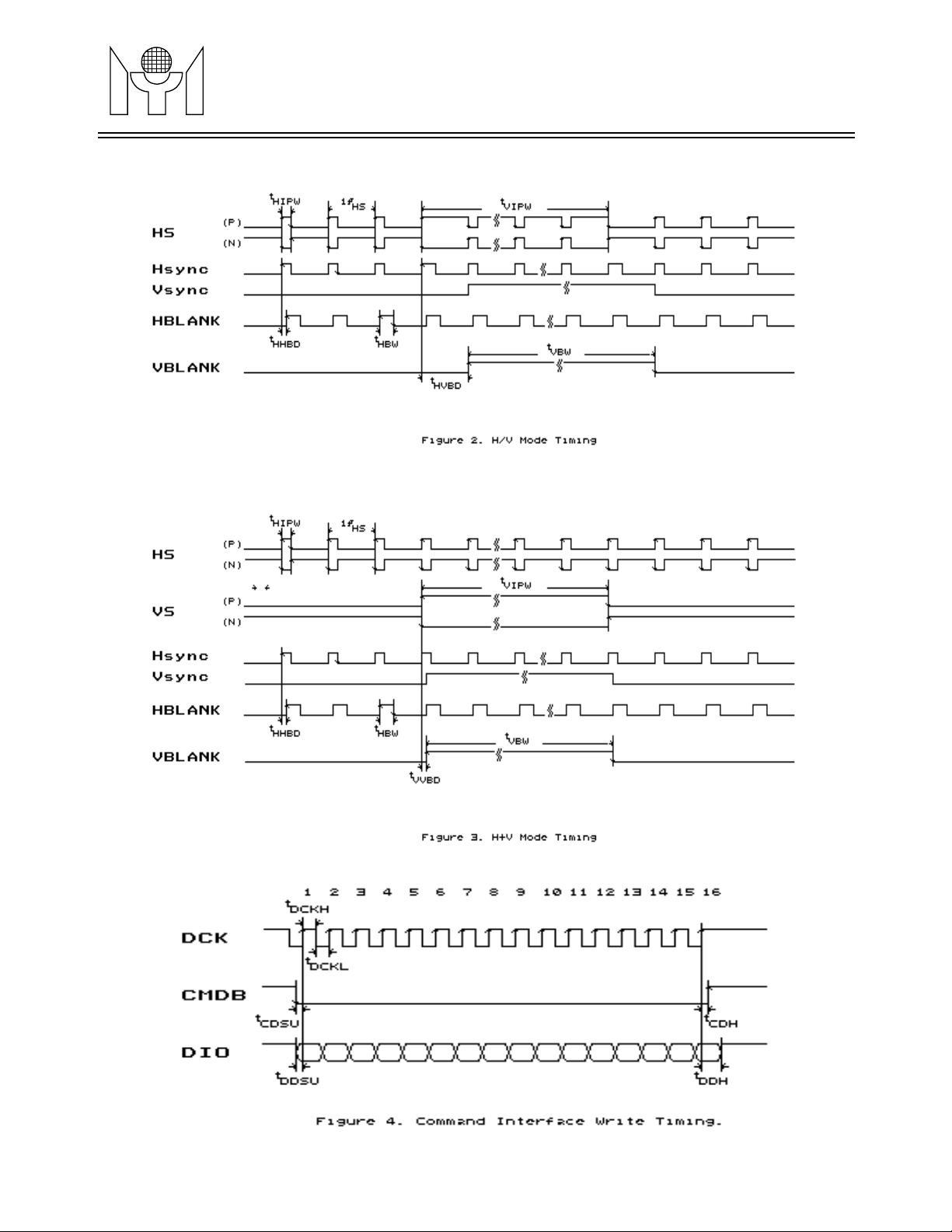
command interface. The timing diagrams of sync processing are shown as Fig. 2 in section 8.0. The internal
SYNC signals (Hsync and Vsync) are extracted from different sources according to the following modes of
operation.
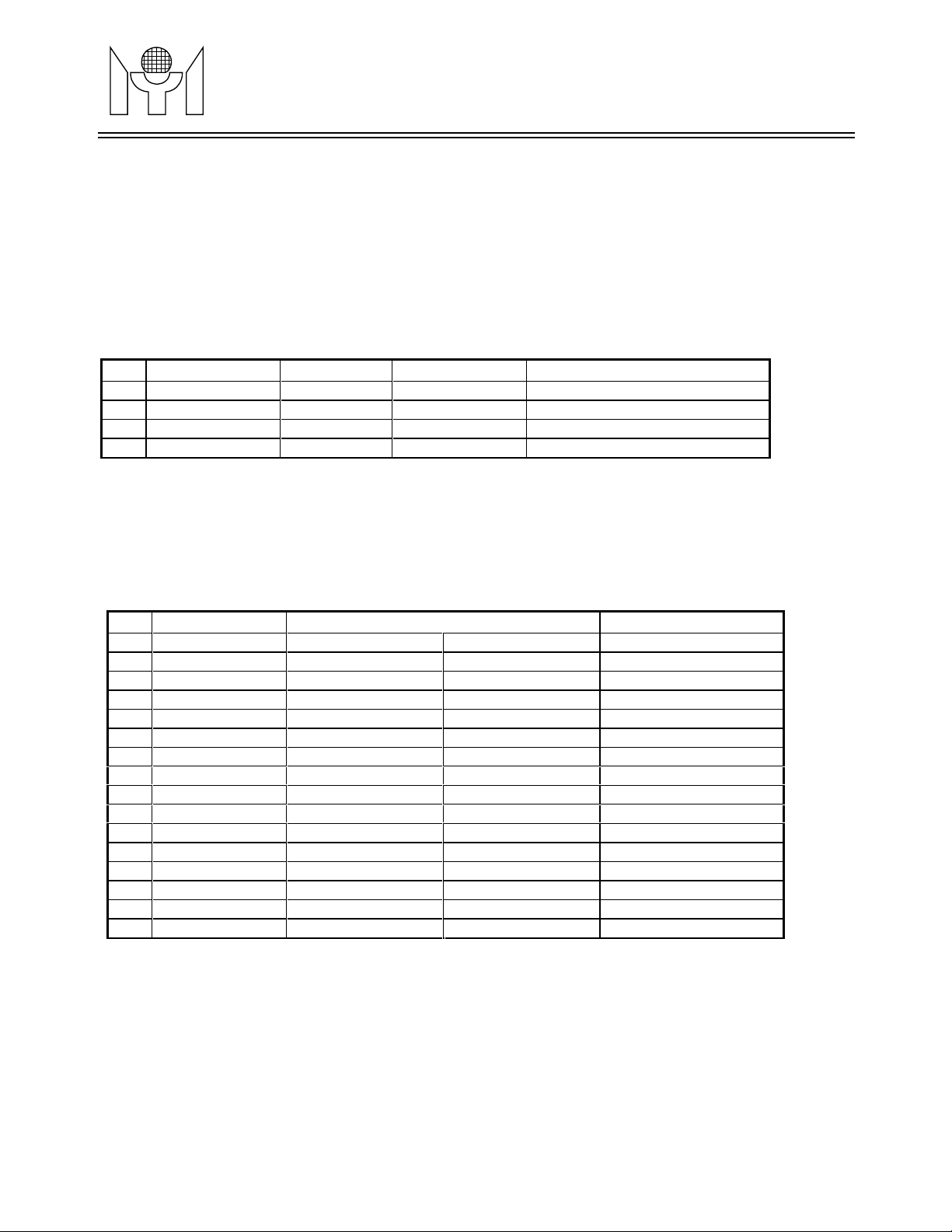
Mode VS HS Comment
1 Separate(H+V) present present HS = H or H/V sync
2 Composite(H/V) not present present HS= H/V sync
3 Suspend present not present 4 Off not present not present -
3.4 H-Freq Table
After the "start H-Freq count" command is issued over 10 ms (for 15.7KHz) and HCFF(H-Freq Count Finished
Flag) is set High, the H-Freq output (HF9 - HF0) is valid. The output value of H-Freq is calculated using the
following formula:
output value = [(1/f
Hfreq(KHz
) x 64 x 4000] / 16
)
(MTV003)
H-Freq(KHz) Output value hexadecimal 11 bits decimal Tolerance (%)
1
15.7 3FB 1019 0.0981354
2
18.7 357 855 0.1169591
3
21.8 2DD 733 0.1364256
4
30 215 533 0.1876172
5
31.5 1FB 507 0.1972386
6
33.5 1DD 477 0.2096436
7
35.5 1C2 450 0.2222222
8
36.8 1B2 434 0.2304147
9
38 1A5 421 0.2375297
10
40 190 400 0.2500000
11
48 14D 333 0.3003003
12
50 140 320 0.3125000
13
57 118 280 0.3571428
14
60 10A 266 0.3759398
15
64 0FA 250 0.4000000
16
100 0A0 160 0.6250000
3.5 V-Freq Table
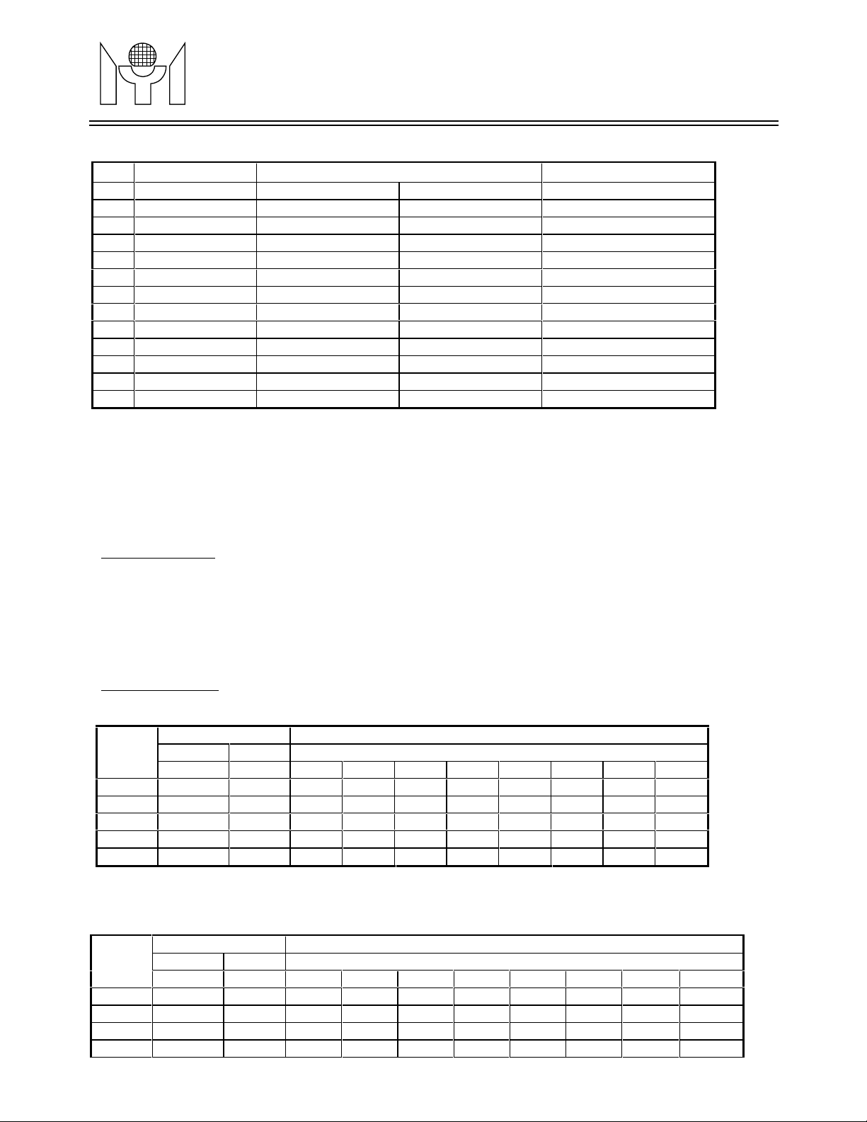
After the "start V-Freq count" command is issued over 120 ms (for 50HZ) and VCFF (V-Freq Count Finish Flag)
is set High, the V-Freq output (VF8 - VF0) is valid. The output value of V-Freq is calculated according to the
following formula:
output value = [(4/f
freq(Hz
V
) x 4000000] / (64 x 16)
)
4/13
MTV003 Revision 2.3 07/01/1998
Page 5
MYSON
MTV003N
TECHNOLOGY
(MTV003)
V-Freq(Hz) Output value hexadecimal 9 bits decimal Tolerance (%)
1 20 30D 781 0.12804
2 56.25 115 277 0.36101
3 59.94 104 260 0.38461
4 60 104 260 0.38461
5 60.32 103 259 0.38610
6 60.53 102 258 0.38759
7 66.67 0EA 234 0.42735
8 70.069 0DE 222 0.45045
9 70.08 0DE 222 0.45045
10 72 0D9 217 0.46082
11 72.378 0D7 215 0.46511
12 72.7 0D6 214 0.46728
13 87 0B3 179 0.55865
3.6 Command Interface
The command interface contains 3 pins. Each transfer of command is comprised of 16 DCK clock periods. The
first 8 DCK clocks are for the address and direction of DIO, and the succeeding 8 DCK clocks are for the data.
Each transfer is initiated by setting CMDB Low. The CMDB pin must be pulled High after data transfer is
completed.
- Command Format
B0 - 4 (
B5 (
ADD4 - 0
W/RB
) : Address of the registers.
) : Transfer direction, 1=write, 0=read.
B6 - 7 : Reserved.
B8 - 15 (
DA0 - 7
DA7 - 0
(
) : Data input when
) Data output when
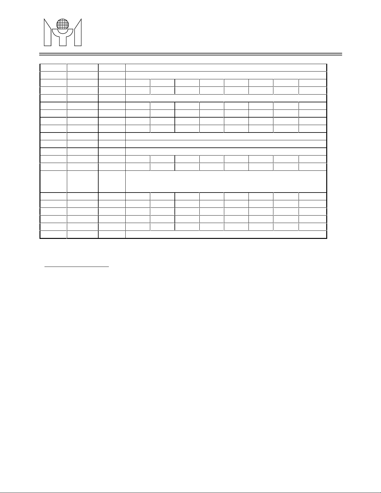
- Register Allocation
a. Read Transfer
Address Portion Data Portion
Reg #
ADD4-0 W/RB DA7 - 0
B0 - 4 B5 B8 B9 B10 B11 B12 B13 B14 B15
Reg0
Reg1
Reg2
Reg3
Reg4
00000 0
00001 0
00010 0
00011 0
00100 0
H
HF7 HF6 HF5 HF4 HF3 HF2 HF1 HF0
VF7 VF6 VF5 VF4 VF3 VF2 VF1 VF0
b. Write Transfer
Address Portion Data Portion
Reg #
ADD4-0 W/RB DA0 - 7
B0 - 4 B5 B8 B9 B10 B11 B12 B13 B14 B15
Reg0
Reg1
Reg2
Reg3
00000 1
00001 1
00010 1
00011 1
V
CLK4MTESTxxxxx x
W/RB
=1.
W/RB
=0.
pol
x x x x HCFF HF10 HF9 HF8
xxxxxxVCFFVF8
V
pol
HS
pre
VS
pre
HV
pre
H
sl
V
sl
x
Table 4
xxxxxxx x
pf0
xxxxxxx x
V
pf1
H
pf0
H
pf1
VB
HB
pl
HV
pl
MTV003 Revision 2.3 07/01/1998
cvs
x
5/13
Page 6
MYSON
MTV003N
Reg4
Reg5
Reg6
Reg7
Reg8
Reg9
Reg10
Reg11
Reg12
Reg13
Reg14
Reg15
Reg16
Reg17
Reg18
I
Reg25
Reg26
Reg27
Reg28
Reg29
Reg30
Reg31
TECHNOLOGY
00100 1
00101 1
00110 1
00111 1
01000 1
01001 1
01010 1
01011 1
01100 1
01101 1
01110 1
01111 1
10000 1
10001 1
10010
I
11001
11010 1
11011 1
11100 1
11101 1
11110 1
11111 1
(MTV003)
Reserved
Reserved
HBD0 HBD1 HBD2 HBD3 HBD4 HBD5 HB D6 HBD7
HBW0 HBW1 HBW2 HBW3 HBW4 HBW5 HBW6 HBW7
Reserved
VBW0 VBW1 VBW2 VBW3 VBW4 VBW5 x VBW7
DA0
DA1
DA2
STF RT0 RT1
XA0
XA1
XA2
XA3
XA4
DA0
b0
DA1
b0
DA2
b0
xxxxxxx x
XA0
b0
XA1
b0
XA2
b0
XA3
b0
XA4
b0
b1
b1
b1
b1
b1
b1
b1
b1
DA0
DA1
DA2
XA0
XA1
XA2
XA3
XA4
b2
b2
b2
b2
b2
b2
b2
b2
DA0
DA1
DA2
ST
XA0
XA1
XA2
XA3
XA4
b3
b3
b3
Reserved
Reserved
Reserved
bsh
Reserved
b3
b3
b3
b3
b3
Reserved
DA0
DA1
DA2
S
XA0
XA1
XA2
XA3
XA4
elft
b4
b4
b4
b4
b4
b4
b4
b4
DA0
DA1
DA2
xx x
XA0
XA1
XA2
XA3
XA4
b5
b5
b5
b5
b5
b5
b5
b5
DA0
DA1
DA2
XA0
XA1
XA2
XA3
XA4
b6
b6
b6
b6
b6
b6
b6
b5
DA0
DA1
DA2
XA0
XA1
XA2
XA3
XA4
b7
b7
b7
b7
b7
b7
b7
b7
* The above x may represent any data.
- Command Descriptions
Reg0 (write) : Begins the H-Freq count. To read the value in the H-Freq registers, the write command (Reg0)
needs to be issued first.
Reg0 (read) : The status of polarity, presence and static level for HS and VS.
1. H
2. HS
3. Hsl, V
* HVpre represents the status of the composite (H/V) presence in HS. Hsl or V
, V
pol
pre
sl
when HS
pol
, VS
pre
= 1 -> positive, = 0 -> negative.
, HVpre = 1 -> present, = 0 -> not present.
pre
= 1 -> high, = 0 -> low.
or VS
is not present.
pre
is valid only
sl
Reg1 (read) : Hfreq Count Finish flags, Hfreq high bit.
1. HCFF = 1 -> valid, = 0 -> not valid.
2. HF10 - HF8 = 3 high bit of Hfreq.
Reg1 (write) : Selects the source of VBLANK and controls the polarity status of H
pol, Vpol
and SYNC output polarity.
1. HV
cvs
= 1 -> VBLANK is extracted from HS.
= 0 -> VBLANK is extracted from VS.
2. HBpl = 1 -> negative HBLANK output, = 0 -> positive HBLANK output.
3. VBpl = 1 -> negative VBLANK output, = 0 -> positive VBLANK output.
* After power-on, HBpl and VBpl shall be initialized to 0.
4. H
5. V
pf1
pf1
, H
, V
= 0,0 or 1,1 -> H
pf0
= 0,1 -> force H
= 1,0 -> force H
= 0,0 or 1,1 -> V
pf0
pol
pol
= x, by auto detection.
= 1.
pol
= 0.
pol
= x, by auto detection.
MTV003 Revision 2.3 07/01/1998
6/13
Page 7

MYSON
MTV003N
TECHNOLOGY
= 0,1 -> force V
= 1,0 -> force V
Reg 2 (read) : H-Freq low byte.
Reg 2 (write) : Begins V-Freq count. To read the value in V-Freq registers, the write command (Reg2) must
be issued first.
Reg3 (read) : V-Freq Count Finish flag, V-Freq high bit.
1. VCFF = 1 -> valid, = 0 -> not valid.
2. VF8 = the high bit of V-Freq.
Reg3 (write) : Controls test and clock modes.
1. TEST = 0 -> Normal mode.
= 1 -> Test mode, not allowed in applications.
2. CLK4M = 0 -> CLK = X1 divided by 2 (for 8MHz crystal power-on [default]).
= 1 -> CLK = X1 (for 4MHz crystal power-on [default]).
Reg4 (read) : V-Freq low byte.
Reg4 (write) : Reserved.
Reg5 (write) : Reserved.
pol
pol
= 1.
= 0.
(MTV003)
Reg6 (write) : Controls the delay of HBLANK output (7 bits).
(HBD7 - 0)
= 10000000 -> Directly bypasses Hsync to output.
= 01000000 -> Min. propagation delay (approximately 300ns).
= 00000000 -> T + 500ns.
= 00000001 -> 2T + 500ns.
= 00111111 -> 64T + 500ns.
Reg7 (write) : Controls the width of HBLANK output (7 bits).
(HBW7 - 0)
= 10000000 -> Directly bypasses Hsync to output.
= 01000000 -> Min. width (approximately 300ns).
= 00000000 -> T + 500ns.
= 00000001 -> 2T + 500ns.
= 00111111 -> 64T + 500ns.
Reg8 (write) : Reserved.
Reg9 (write) : Controls the width of Vblank output (7 bits).
(VBW7 - 0)
= 1-000000 -> Directly bypasses Vsync to output.
= 0-000000 -> Min. width (approximately 8us).
= 0-000001 -> 16 + 8(us).
= 0-111111 -> 16 * 63 + 8(us) = 1.016ms.
Reg10 (write) : Output pulse width control for DA0.
Reg11 (write) : Output pulse width control for DA1.
Reg12 (write) : Output pulse width control for DA2.
Reg13 (write) : Reserved.
MTV003 Revision 2.3 07/01/1998
7/13
Page 8

MYSON
MTV003N
TECHNOLOGY
Reg14 (write) : Reserved.
Reg15 (write) : Reserved.
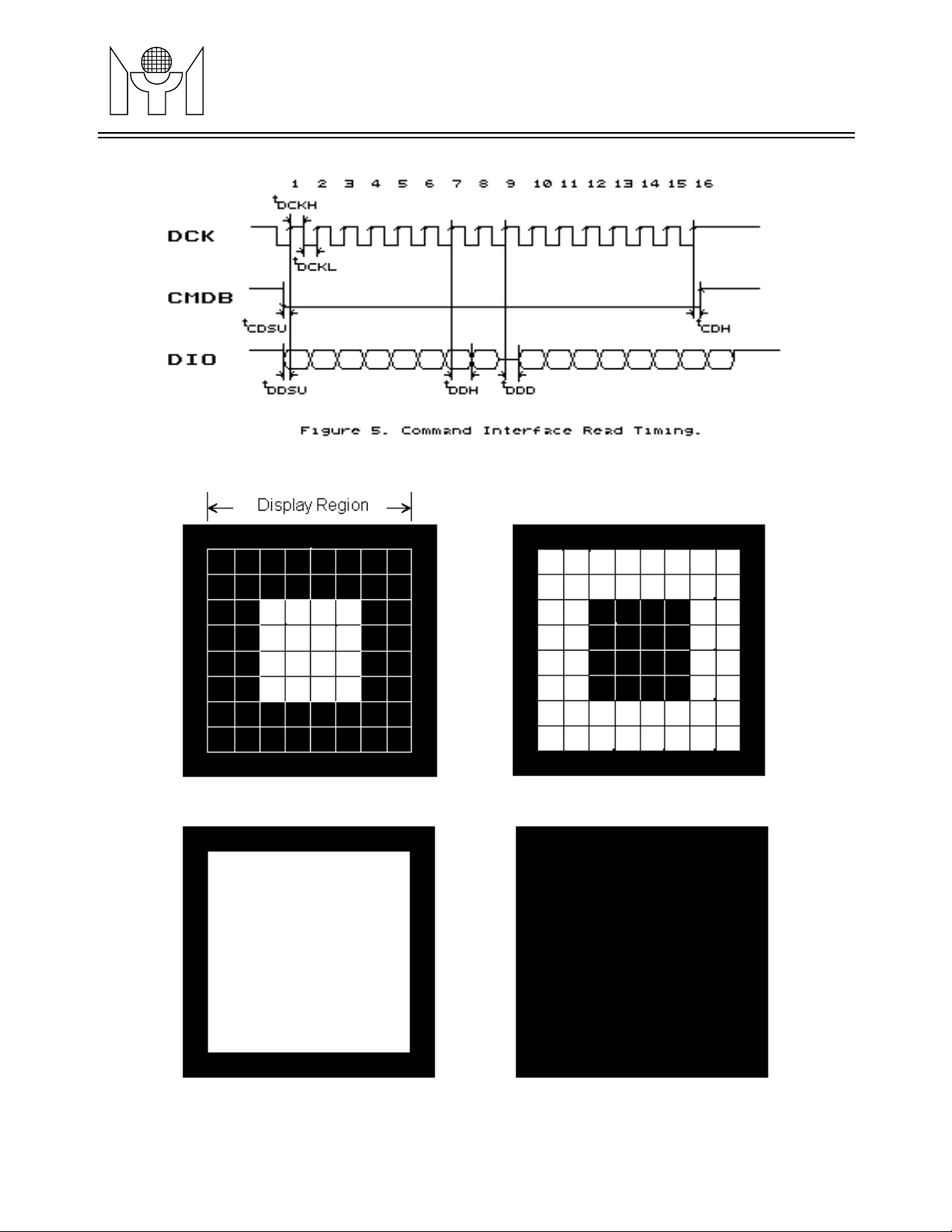
Reg16 (write) : Controls i) enabler, ii) band selection, iii) 4 pattern modes and iv) output enabler
for the self-test pattern generator.
1. S
elft
2. ST
bsh
3. RT1, RT0 = 0,0 -> Positive cross-hatch pattern output.
4. STF= 1 -> Enables STOUT output.
Reg17 (write) : Reinitializes all internal registers.
Reg26 (write) : Output pulse width control for XDA0.
= 1 -> Enables generator.
= 0 -> Disables generator.
= 1 -> 63.5KHz (horizontal) output selected.
= 0 -> 31.75 KHz (horizontal) output selected.
= 0,1 -> Negative cross-hatch pattern output.
= 1,0 -> Full white pattern output.
= 1,1 -> Full black pattern output.
= 0 -> Disables STOUT output.
(MTV003)
Reg27 (write) : Output pulse width control for XDA1.
Reg28 (write) : Output pulse width control for XDA2.
Reg29 (write) : Output pulse width control for XDA3.
Reg30 (write) : Output pulse width control for XDA4.
Reg31 (write) : Reserved.
*1. The above T = 250ns.
2. All D/A converters are centered with a value of
low after power-on or a Reg17 write .
3. The duration of power-on initialization is 200ms and Reg17 write reinitiation is 2.5ms. No register access is
allowed during initialization.
DA7 - 0
= 10000000, and other registers are initialized with
8/13
MTV003 Revision 2.3 07/01/1998
Page 9
MYSON
MTV003N
TECHNOLOGY
4.0 ABSOLUTE MAXIMUM RATINGS
DC Supply Voltage (VDD) -0.3 to 7 V
Voltage with respect to Ground:
All pins except VDD and DA0 to DA2 -0.3 to VDD+ 0.3 V
DA0 to DA2 -0.3 to +13.2 V
Storage Temperature -65 to +150 oC
Ambient Operating Temperature 0 to +70 oC
5.0 OPERATING CONDITIONS
DC Supply Voltage (VDD) +4.75 V to +5.25 V
External D/A Power Supply +5 V to 12 V
Operating Temperature 0 to +70 oC
6.0 ELECTRICAL CHARACTERISTICS (Under Operating Conditions)
(MTV003)
Symbol Parameter Conditions (Notes) Min. Max. Unit
V
IH
V
IL
V
OH
V
OL
V
DAOL
V
DAOH
I
CC
Input High Voltage
Input Low Voltage
Output High Voltage
Output Low Voltage
Open-Drain D/A
Output Low Voltage
Open-Drain D/A
Output High Voltage
Maximum Quiescent
Supply Current
-
(for all input pins)
-
(for all input pins)
IOH = -500 uA
(for pins of HBLANK,
VBLANK, DIO, Bout, STOUT,
XDA4-0)
I
= 4 mA
O
L
(see VOH)
IDAOL = 3 mA
(for pins of DA2-0)
-
(for pins of DA2-0, pulled up
by external 5 to 12V power
supply)
Vin = VDD,
Iout = 0 uA.
(all input pins connected to
VDD, all output pins without
connection)
2.4
VSS-0.3 0.8 V
3.0 - V
-0.5V
-0.35V
512V
-20mA
VDD+
0.3
V
9/13
MTV003 Revision 2.3 07/01/1998
Page 10
MYSON
MTV003N
TECHNOLOGY
(MTV003)
7.0 SWITCHING CHARACTERISTICS (Under Operating Conditions and X1=8MHz)
Symbol Parameter Min. Typ. Max. Unit
f
DAO
f
XTAL
f
HS
f
VS
t
HIPW
t
VIPW
t
HHBD
t
HBW
t
HHBJ
t
VBW
t
HVBD
t
VVBD
t
VVBJ
t
HVBJ
t
CDSU
t
CDH
t
DDSU
t
DDH
t
DCKH
t
DCKL
T
DDD
D/A Converter Output
Frequency
Crystal Frequency - 8 - MHz
HS Input Frequency 15 - 100 KHz
VS Input Frequency 20 - 100 Hz
HS Input Pulse Width 0.5 - 6.5 us
VS Input Pulse Width 25 - 2000 us
HSYNC (Rise) to HBLANK
Output Delay
(programmed by Reg6)
HSYNC (Rise) to HBLANK
Output Delay
(bypass HSYNC to HBLANK
Output directly)
HBLANK Output Width
(programmed by Reg7)
HBLANK Output Width
(bypass HSYNC to HBLANK
Output directly)
HSYNC to HBLANK Output
Jitter
VBLANK Output Width
(programmed by Reg9)
VBLANK Output Width
(bypass VSVNC to VBLANK
Output directly)
HSYNC to VBLANK Output
Delay
(H/V mode)
VS to VBLANK Output Delay
(H+V mode)
VSYNC to VBLANK Output
Jitter(H+V mode)
HSYNC to VBLANK Output
Jitter (H/V mode)
CMDB to DCK Setup Time 200 - - ns
CMDB to DCK Hold Time 100 - - ns
DIO to DCK Setup
Time (write)
DIO to DCK Hold Time(write) 100 - - ns
DCK High Time 200 - - ns
DCK Low Time 200 - - ns
DCK to DIO Delay Time(read) 100 - - ns
- 31.25 - KHz
300 (N+1)xT+500 64xT+850 ns
- - 50 ns
300 (N+1)xT+500 64xT+850 ns
0.5 - 7 us
- - (+/-) 25 ns
16 (Nx16)+8 1016 us
25 - 2000 us
-1 H-line--
- - 50 ns
- - (+/-) 25 ns
- - (+/-) 25 ns
200 - - ns
* 1. The above HSYNC is extracted from HS input and VSYNC is extracted from VS, HS input.
* 2. T = 250ns (1/4MHz) is fixed regardless of whether or not an 8(or 4)MHz crystal is used.
* 3. 0 < N <
63
MTV003 Revision 2.3 07/01/1998
10/13
Page 11
MYSON
MTV003N
TECHNOLOGY
8.0 TIMING DIAGRAMS
(MTV003)
11/13
MTV003 Revision 2.3 07/01/1998
Page 12
MYSON
MTV003N
TECHNOLOGY
(MTV003)
Figure 6. 4 Self-Test Patterns
12/13
MTV003 Revision 2.3 07/01/1998
Page 13
MYSON
MTV003N
TECHNOLOGY
(MTV003)
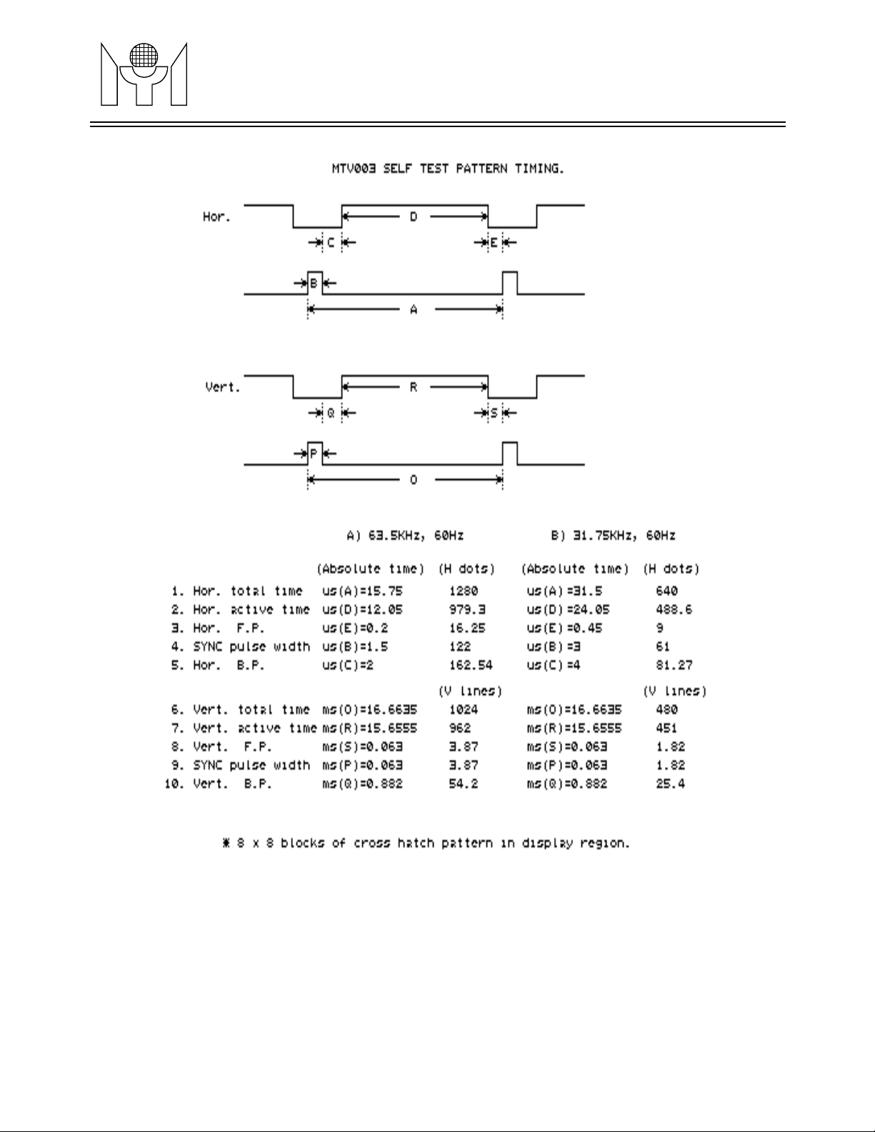
Figure 7. Self-Test Timing
13/13
MTV003 Revision 2.3 07/01/1998
 Loading...