

Page 1
MYSON
TECHNOLOGY
MTU420
4-Bit Micro-Controller with LCD Driver, 2K Word
FEATURES
Wide operati ng vol tage range:
•
Supply Vol tage Cycle Time Clock Usage Remark
4.5V to 5.5V
4V to 5V
2.4V to 3.3V
1.2V to 1.65V
118 instruction sets:
•
122µs,280ns
122µs,280ns
122µs,2.2us
122µs
- Binary addition, subtr ac tion, BCD adjustment, logical operati on in direct addr essing mode and index
addressing mode.
- Single- bit m anipulation (set, reset, dec ision for br anc h) .
- 4-bit input/output.
- Various conditional br anc hes.
- 16 working registers and manipulation.
- LCD driver data t r ansfer.
- Look-up table.
- Programmable opt ion.
- System clock selection.
8-level subroutine nesting.
•
Interrupt function:
•
- Exter nal fac tor: 2 (INT pin or ports S, M ) .
- Internal factor: 2 (timer, divider).
ROM/RAM capac ity:
•
- ROM capaci ty . . . . . 2048 x 16 bits.
- RAM capacity . . . . . 128 x 4 bits.
Watchdog timer.
•
Input/Output ports:
•
- Input ports . . . . . 2 por ts/8pins (S, M).
- Output port . . . . . 1 port/4pins (P).
- Pseudo serial output por t . . . . . Also used for output port.
- Input/Output ports . . . . . 2 ports/8pins (I/OA, I/OB).
2 control outputs . . . . . light, alarm.
•
LCD driver output:
•
- 26 LCD driver output s (up t o 156 LCD segments are drivable) .
- Mask option i s used to select static ½ duty, ½ bias ½ dut y , ½ bias 1/3 duty, ½ bias ¼ duty, 1/3 bias
1/3 duty, ½ bias ¼ duty and 1/3 bi as 1/6 duty drive modes of the LCD panel .
- Mask option permits LCD driver output pins to be used for output port s.
- Segment P LA c ircuit permi ts any layout on t he LCD panel.
Built - in doubler, halv er , tripler.
•
One 6-bit tim er with programmable option clock.
•
128-byte look- up table for LCD display pat tern or 256-nibble look-up t able for gener al purpose.
•
Halt function.
•
Stop func tion.
•
Dual clock oper ation.
•
dual clock Max. 3. 58M Hz
dual clock Max. 3. 58M Hz
dual clock Max. 455KHz
slow clock only 32.768KHz
This datasheet contains new product information. Myson Technology reserves the rights to mo dify the product specification without notice.
No liability is a ssumed as a result of the use o f this product. No rights under any patent accompany the sale of the product.
1/11 MTU420 Revision 2.9 02/17/19981/11
Page 2
MYSON
TECHNOLOGY
MTU420
GENERAL DESCRIPTION
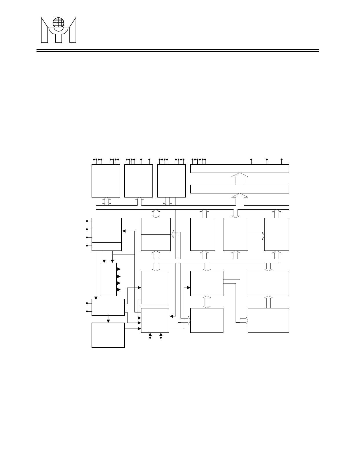
The MTU420 is an LCD driv er with an embedded high- per formance 4-bit micr oc omputer. It contains all the
necessary functions in a single chip: dual clock, 4-bit parallel processing ALU, ROM, RAM, input/ output
ports, timer, clock generator, LCD driver, look-up tabl e and watchdog timer . The set of 118 instructi ons
includes not only 4-bit oper ation and manipulation instruct ion but also various conditional branch
instructions, and LCD driver data t r ansfer instruc tions that are powerful and easy to follow. T he halt function
stops internal operations other than the oscillator, divider and LCD driver in order to minimize power
dissipation. The stop function stops all c locks in the c hip.
BLOCK DIAGRAM
I/O
A1~4
DIRECTION
I/O
B1~4
BI-
I/O PORT
P1~4
OUTPUT
PORT
S1~4 M1~4 COM1~6
LIGHT
ALARM
INPUT
PORT
26 SEGMENTS
VDD1 VDD2 VDD3
LCD DRIVE
SEGMENT PLA
XTOUT
CFOUT
CUP1
CUP2
XTIN
CFIN
OSC
CKT
WAIT CNT
T1
SCG
PREDIVIDER
WATCHDOG
TIMER
T2
T3
T4
AC
DAA
ALU
6-BIT
PRESET
TIMER
CONTROL
CIRCUIT
RES INT
LOOK-UP
TABLE
128x8
11-BIT PC
STACK 8
LEVELS
INDEX
BUFFER
RAM
(128x4)
INSTRUCTION
DECODE
ROM (2048x16)
2/11
MTU420 Revision 2.9 02/17/1998
Page 3
MYSON
TECHNOLOGY
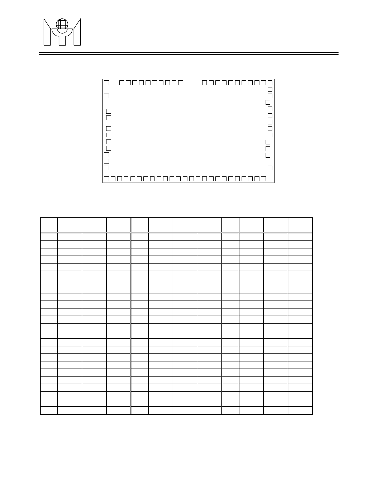
1.0 CONNECTION DIAGRAM
30
40 6050
2.0 PIN ASSIGNMENT
MTU420
1020
Pad No. 1
69
Pin
No.
10 IOA2 3599.5 2770.5 34 CFIN 154.5 980.5 58 SEG20
11 IOA3 3439.5 2770.5 35 CFOUT 154.5 1140.5 59 SEG21 3312.5 125.5
12 IAO4 3279.5 2770.5 36 COM1 133 730.5 60 SEG22 3472.5 125.5
13 IOB1 3119.5 2770.5 37 COM2 133 570.5 61 SEG23 3632.5 125.5
14 IOB2 2959.5 2770.5 38 COM3 133 410.5 62 SEG24 3792.5 125.5
15 IOB3 2799.5 2770.5 39 SEG1 112.5 125.5 63 SEG25 3952.5 125.5
16 IOB4 2639.5 2770.5 40 SEG2 272.5 125.5 64 SEG26 4112.5 225.5
17 RES 2479.5 2770.5 41 SEG3 432.5 125.5 65 COM4 4092 461
18 INT 1862.5 2770.5 42 SEG4 592.5 125.5 66 COM5 4092 621
19 P1 1702.5 2770.5 43 SEG5 752.5 125.5 67 COM6 4092 781
20 P2 1542.5 2770.5 44 SEG6 912.5 125.5 68 VDD3 4127 981
21 P3 1382.5 2770.5 45 SEG7
22 P4 1222.5 2770.5 46 SEG8 1232.5 125.5
23 M1
24 M2 902.5 2770.5 48 SEG10 1552.5 125.5
*Note: The substrate of die must connect to GND.
Pin
NameX(um)Y(um)
1 VDD 4127 1311 25 M3 742.5 2770.5 49 SEG11 1712.5 125.5
2 VDD1 4110.5 1471 26 M4 582.5 2770.5 50 SEG12 1872.5 125.5
3 VDDO 4110.5 1631 27 TESTA 422.5 2770.5 51 SEG13 2032.5 125.5
4 VDD2 4078 1791 28 CUP1 109 2757 52 SEG14 2192.5 125.5
5 ALM 4127 2142.5 29 CUP2 109 2190 53 SEG15 2352.5 125.5
6 LIGHT 4127 2440.5 30 S2 154.5 1891 54 SEG16 2512.5 125.5
7 S4 4079.5 2700.5 31 S1 154.5
8 S3 3919.5 2770.5 32 XTIN 154.5 1460.5 56 SEG18 2832.5 125.5
9 IOA1 3759.5 2770.5 33 XTOUT 154.5 1300.5 57 SEG19 2992.5 125.5
1062.5
2770.5 47 SEG9 1392.5 125.5
Pin
No.
Pin
NameX(um)Y(um)
1072.5
Pin
No.
1725.5
125.5 69 GND 4127 1151
55 SEG17 2672.5 125.5
Pin
NameX(um)Y(um)
3152.5
125.5
3/11
MTU420 Revision 2.9 02/17/1998
Page 4
MYSON
TECHNOLOGY
3.0 PIN DESCRIPTIONS
Name Type Description
XTIN
XTOUT
CFIN I - System clock oscillation.
CFOUT O - Connected with ceramic resonator or crystal oscillator.
S1 - 4 I - Input port.
M1 - 4 I - Input port.
IOA1-4 I/O - Input/ Output port.
IOB1-4 I/O - Input/ Output port.
P1 - 4 O - Output port.
INT I - Input port.
VDD - Positive supply voltage.
LIGHT O - Output port.
ALM O - Out put port.
RES I - Input pin from LSI r eset r equest si gnal.
GND - Negative supply voltage.
VDD3
VDD2
VDD1
I
- Time-based counter frequency (cl oc k specified, LCD alter nating frequency,
O
alarm signal frequency) or system cl ock oscillation.
- 32KHz crystal oscillator.
- Oscillation stops at the execution of stop instruction.
- Connected with RC oscillation circuit.
- Oscillation stops at the execution of stop or SLOW instruction.
- Input pins for data storage into RAM area (wit h c hattering pr evention).
- Internal c hattering pr evention circ uit (32m s, 8ms, 2ms selectable by
applicat ion program ) .
- Internal pull-down resistor (sel ec table by applicati on pr ogr am).
- Internal " L"-level logic holds Tr ( sel ec table by mask option).
Note: The chat tering prevention circuit param eters, 32ms, 8ms and 2ms, apply
to the 32.768KHz fundam ental f r equenc y input m ode.
- Input pins for data storage into RAM area.
- Internal c hattering pr evention circ uit (32m s, 8ms, 2ms selectable by
applicat ion program ) .
- Internal pull-down resistor (sel ec table by applicati on pr ogr am).
- Internal " L"-level logic holds Tr ( sel ec table by mask option).
Note: The chat tering prevention circuit param eters, 32ms, 8ms and 2ms, apply
to the 32.768KHz fundam ental f r equenc y input m ode.
- Input pins for data storage into the RAM area.
- Output pin for data reading from t he RA M ar ea.
- Input pins for data storage into the RAM area.
- Output pin for data reading from t he RA M ar ea.
- Output pin for data output from t he RA M ar ea.
- Input pin for external request si gnal.
- Interrupt detection si gnal edge selecti on by mask option: falling edge and
rising edge.
- Internal pull-down and pull-up resistor (selectable by mask option).
Note: When using Li version, a capacit or must be connected acr oss GND and
VDD to prevent the logic unit from malfunctioning.
- Output alarm signal: modulated signal s with a frequency of 4kHz, 2k Hz or
1kHz. In this case, these modul ated frequencies are generated and then
outputted i f the fundament al fr equenc y is 32.768kHz.
- Internal pull-down resistor.
- LCD drive voltage.
MTU420
4/11
MTU420 Revision 2.9 02/17/1998
Page 5
MYSON
TECHNOLOGY
Name Type Description
VDDO - Positive supply vol tage.
* For Ag version, apply positive supply vol tage to VDD1. F or other than Ag
versi on, apply posit iv e suppl y voltage to VDD2.
CUP1 - 2 O - S witching pins for supplyi ng the LCD driving voltage to the VDD1 and
VDD2 pins.
- Connect the CUP1 and CUP2 pins with the nonpolar ized elect r olyti c c apac itor
if 1/2 or 1/3 bias mode has been selected.
- In the static mode, these pins should be lef t open.
COM1 - 6 O - Output pins f or suppl y ing voltage to dr ive the common pins of the LCD panel.
- Frequency can be doubled or quadrupled wit h P LA .
SEG1 - 26 O - Output pins for LCD panel segm ents.
* Also used as output ports with m ask opt ion.
TESTA * - Test signal input pin.
MTU420
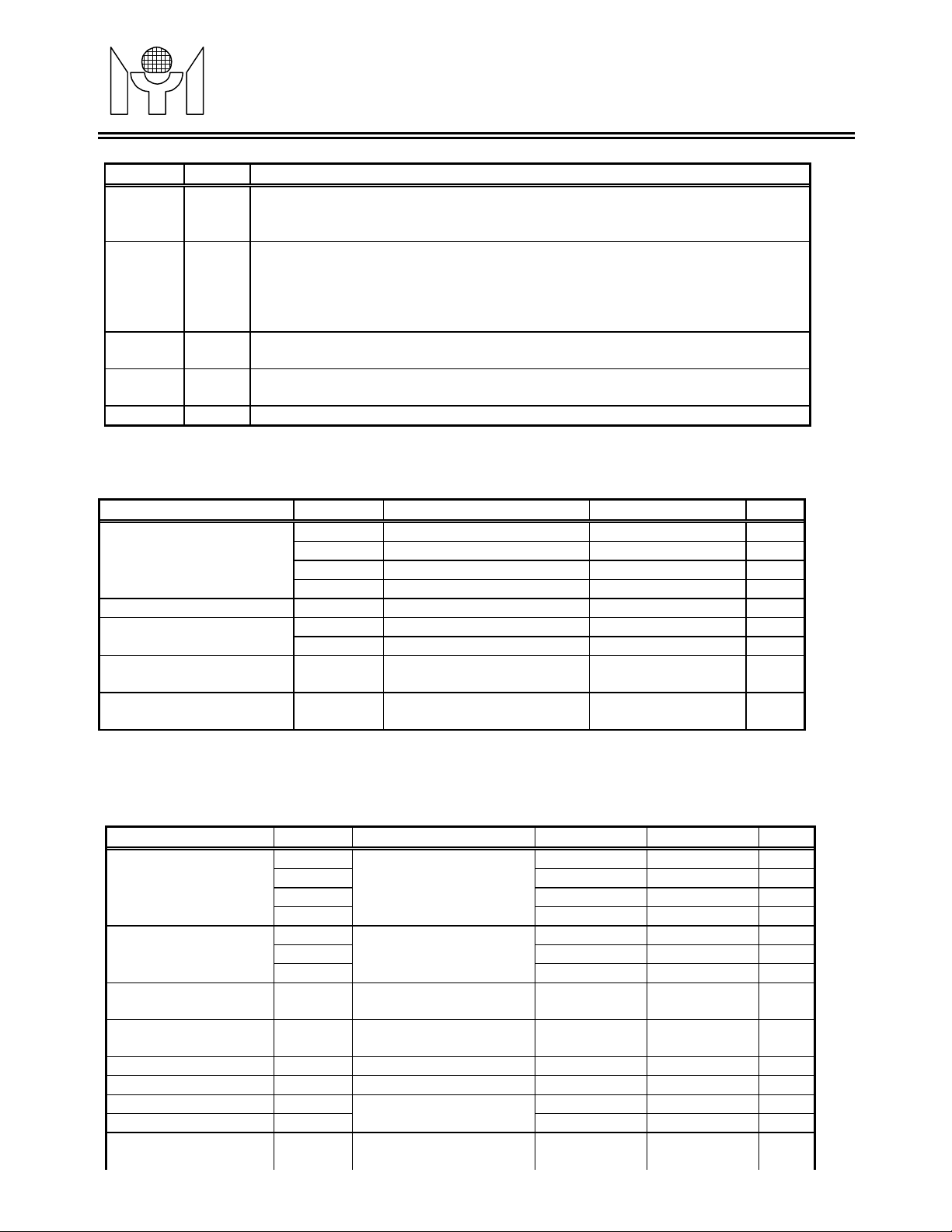
4.0 ABS OLUTE MAXIMUM RATINGS
at GND = 0V
Name Symbol Condition Range Unit
VDD1 -0.3 to 5.5 V
Maximum S upply Volt age
Maximum Input Volt age Vin1 -0.3 to VDDO+0.3 V
Maximum Output Voltage
Maximum Operating
Temperature
Maximum Storage
Temperature
VDD2 -0.3 to 5.5 V
VDD3 -0.3 to 8.5 V
VDDO -0.3 to 5.5 V
Vout1 out put port -0.3 to VDDO+0.3 V
Vout2 LCD segm ent driver -0.3 to VDD3+ 0.3 V
Topg 0 to +70
Tstg -25 to +125
o
o
C
C
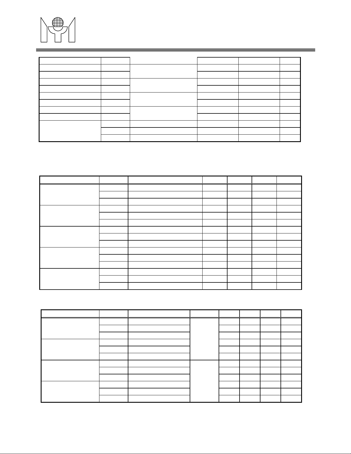
5.0 ALLOWABLE OPERATING CONDITIONS
at Ta = 0 to 70oC, GND = 0V
Name Symb. Condition Min. Max. Unit
VDD1 1.5 5.25 V
Supply Vol tage
Oscillator Start-Up
Voltage
Oscillator Sustain
Voltage
Supply Vol tage VDD1 Ag Mode 1.2 1.65 V
Supply Vol tage VDD2 EXT-V, Li 2.4 5.25 V
Input "H" Voltage Vih1 VDD1-0.7 VDD1+0.7 V
Input "L" Voltage Vil1
Input "H" Voltage Vih2 Li Battery M ode V DD2- 0.7 VDD2+0.7 V
VDD2 3.5 5.25 V
VDD3 3.5 8.0 V
VDDO
VDD1 1.2 5.25 V
VDD2 2.4 5.25 VSupply Vol tage
VDD3
VDD Crystal Mode 1.3 V
VDD Crystal Mode 1.2 V
External RC Mode
1.5 5.25 V
Crystal Mode
2.4 8.0 V
Ag Battery Mode
-0.7 0.7 V
MTU420 Revision 2.9 02/17/1998
5/11
Page 6
MYSON
TECHNOLOGY
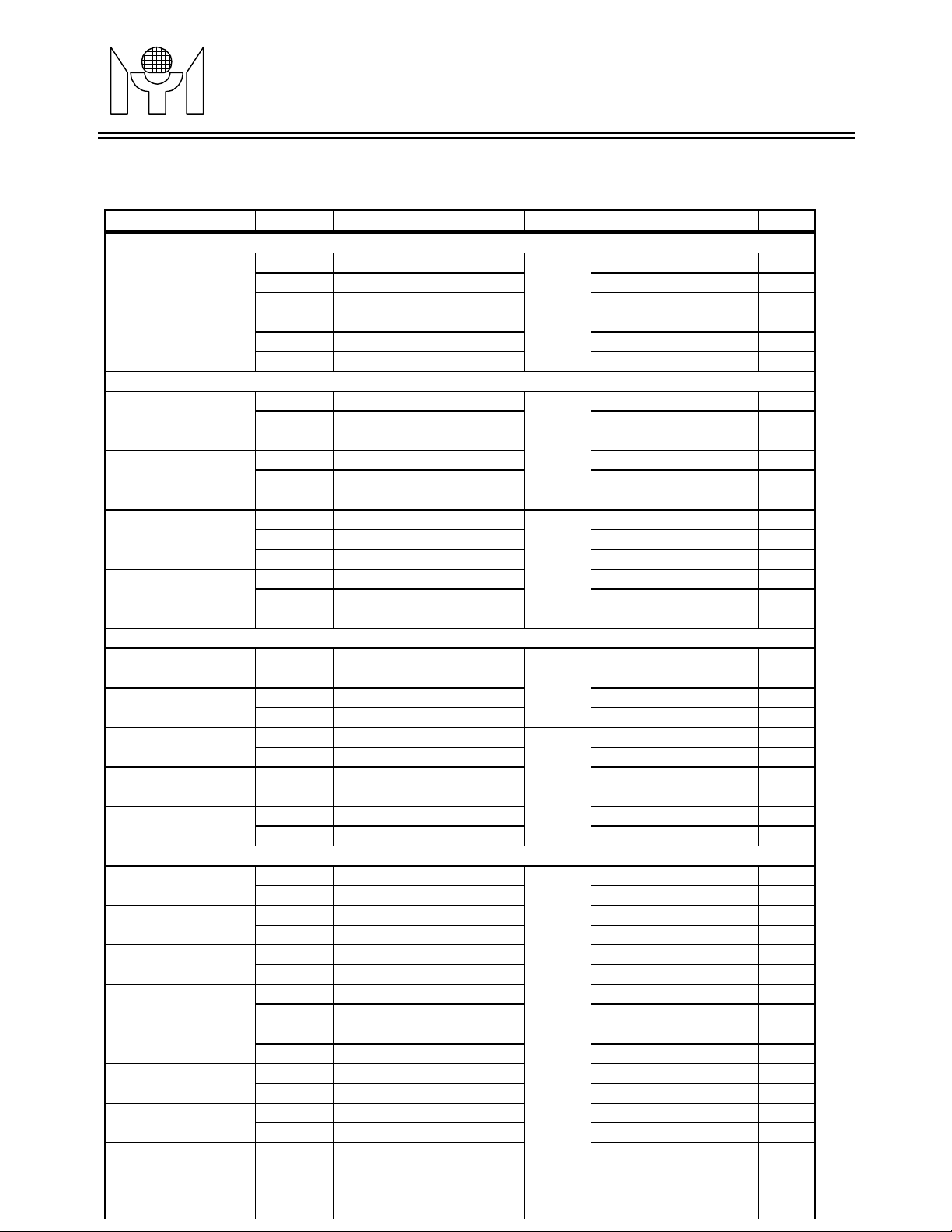
Input "L" Voltage Vil2 -0.7 +0.7 V
Input "H" Voltage Vih3 0.8 x VDD1 VDD1 V
Input "L" Voltage Vil3
Input "H" Voltage Vih4 0.8 x VDD2 VDD2 V
Input "L" Voltage Vil4
Input "H" Voltage Vih5 0.8 x VDD2 VDD2 V
Input "L" Voltage Vil5
Input "H" Voltage Vih6 0.8 x VDDO VDDO V
Input "L" Voltage Vil6
Fopg1 Crystal M ode 32 3580 KHz
Fopg2 External RC Mode 32 1000 KHzOperating Freq.
Fopg3 CF Mode 1000 3580 KHz
OSCIN & Ag Battery
Mode
OSCIN & Li B attery
Mode
CFIN at Li Battery or
EXT-V Mode
RC Mode
0 0.2 x VDD1 V
0 0.2 x VDD2 V
0 0.2 x VDD2 V
0 0.2 x VDDO V
MTU420
6.0 ELECTRICAL CHARACTERISTICS
6.1 Input Resistance
at #1: VDD1 = 1.2V (Ag); #2: VDD2 = 2.4V (Li); #3: VDD2 = 4V (ExtV).
Name Symb. Condition Min. Typ. Max. Unit
Rllh1 Vi = 0.2VDD1, #1 10 50 200 Kohm
Rllh2 Vi = 0.2VDD2, #2 10 40 100 Kohm"L"-Level Hold Tr
Rllh3 Vi = 0.2VDD2, #3 5 20 50 Kohm
Rmsd1 Vi = VDD1, #1 200 700 2000 Kohm
Rmsd2 Vi = VDD2, #2 200 500 1000 KohmM/S Pull-Down Tr
Rmsd3 Vi = VDD2, #3 100 250 500 Kohm
Rintu1 Vi = VDD1, #1 200 700 2000 Kohm
Rintu2 Vi = VDD2, #2 200 500 1000 KohmINT Pull-Up Tr
Rintu3 Vi = VDD2, #3 100 250 500 K ohm
Rintd1 Vi = GND, #1 200 700 2000 Kohm
Rintd2 Vi = GND, #2 200 500 1000 KohmINT Pull-Down Tr
Rintd3 Vi = GND, #3 100 250 500 Kohm
Rres1 Vi = GND or VDD1, #1 5 20 50 Kohm
Rres2 Vi = GND or VDD2, #2 5 20 50 KohmRES Pull-Down R
Rres3 Vi = GND or VDD2, #3 5 20 50 Kohm
6.2 DC Outp ut Characterist ics
at #1: VDD1 = 1.2V (Ag); #2: VDD2 = 2.4V ( Li); #3: V DD2 = 4V (Ex tV).
Name Symb. Condition Port Min. T yp. Max. Unit
Voh1a Ioh = -200uA, #1 -0.5 -0.3 -0.1 V
Voh2a Ioh = -1m A , #2 -1 -0.6 -0.3 VOutput "H" V oltage
Voh3a Ioh = -3m A , #3 -1.5 -1.0 -0.5 V
Vol1a Iol = 400uA, #1 -1.1 -0.9 -0.7 V
Vol2a I ol = 2mA, #2 -2.1 -1.8 -1.4 VOutput "L" Voltage
Vol3a Iol = 6mA, #3
Voh1b Ioh = -100uA, #1 -0.5 -0.3 -0.1 V
Voh2b Ioh = -500uA, #2 -1 -0.6 -0.3 VOutput "H" V oltage
Voh3b Ioh = -1.5mA, #3 -1.5 -1.0 -0.5 V
Vol1b Iol = 200uA, #1 -1.1 -0.9 -0.7 V
Vol2b I ol = 1mA, #2 -2.1 -1.8 -1.4 VOutput "L" Voltage
Vol3b Iol = 3mA, #3
6/11
Alarm
Light
-3.5 -3.0 -2.5 V
P-port
IOA-n
IOB-n
-3.5 -3.0 -2.5 V
MTU420 Revision 2.9 02/17/1998
Page 7
MYSON
TECHNOLOGY
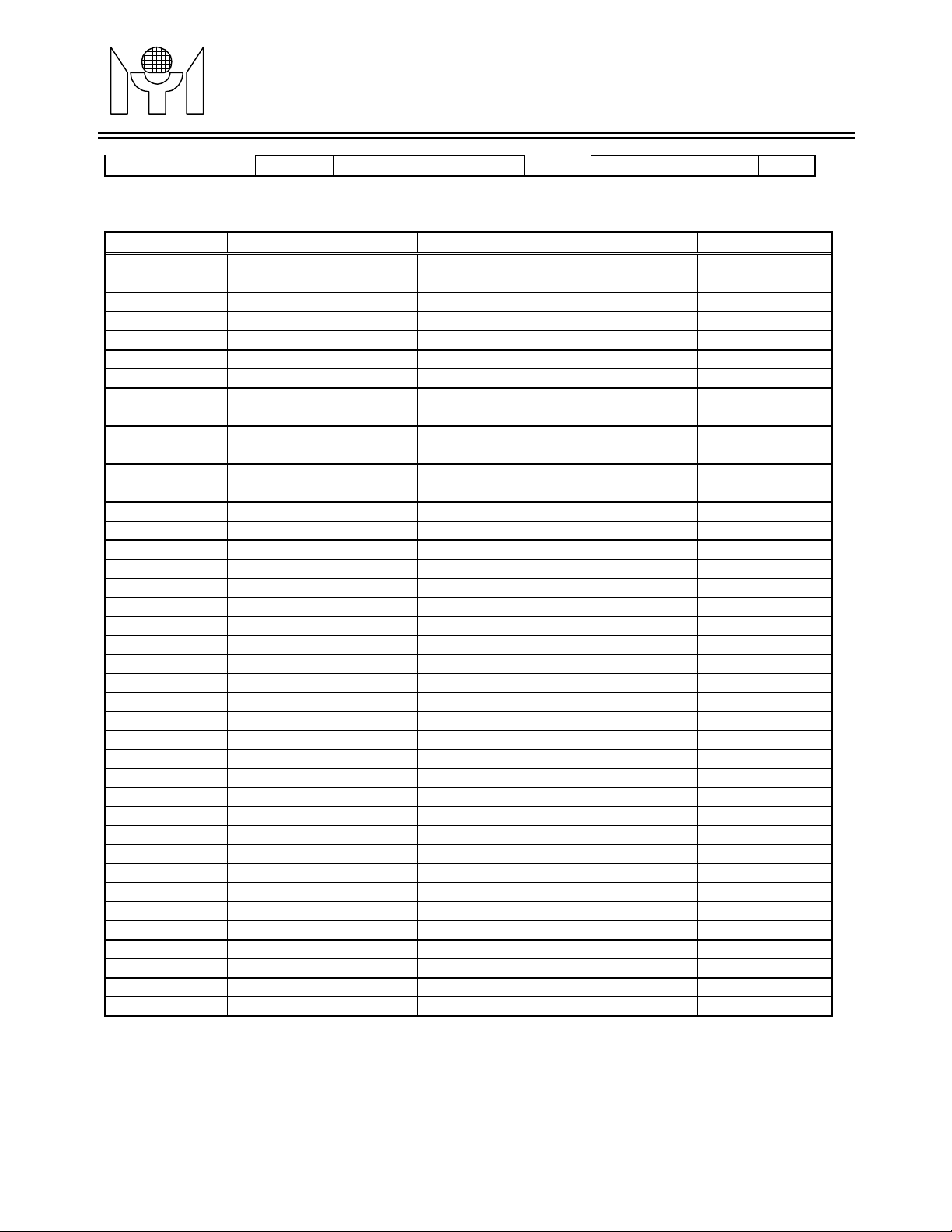
6.3 Segment Driver Outp ut Characteristics
at #1: VDD1 = 1.2V (Ag); #2: VDD2 = 2.4V ( Li); #3: V DD2 = 4V (Ex tV).
Name Symb. Condition for Min. T yp. Max. Unit
CMOS Output Mode
Output "H" V oltage
Output "L" V oltage
Output "H" V oltage
Output "L" V oltage
Output "H" V oltage
Output "L" V oltage
Output "H" V oltage
Output "L" V oltage
Output "H" V oltage
Output "M" Voltage
Output "L" V oltage
Output "H" V oltage
Output"M1" Voltage
Output"M2" Voltage
Output "L" V oltage
Output "H" V oltage
Output"M1" Voltage
Output"M2" Voltage
Output "L" V oltage
Voh1c
Voh2c
Voh3c
Vol1c
Vol2c
Vol3c
Voh1d
Voh2d
Voh3d
Vol1d
Vol2d
Vol3d
Voh1e
Voh2e
Voh3e
Vol1e
Vol2e
Vol3e
Voh12f
Voh3f
Vol12f
Vol3f
Voh12g
Voh3g
Vom12g
Vom3g
Vol12g
Vol3g
Voh12j
Voh3j
Vom12j
Vom13j
Vom22j
Vom23j
Vol2j
Vol3j
Voh2k
Voh3k
Vom12k
Vom13k
Vom22k
Vom23k
Vol2k
Ioh = -10uA, #1
Ioh = -50uA, #2
Ioh = -200uA, #3
Iol = 20uA , #1
Iol = 100uA , #2
Iol = 400uA , #3
Static Disp lay Mode
Ioh = -1uA, #1
Ioh = -1uA, #2
Ioh = -1uA, #3
Iol = 1uA , #1
Iol = 1uA , #2
Iol = 1uA , #3
Ioh = -10uA, #1
Ioh = -10uA, #2
Ioh = -10uA, #3
Iol = 10uA , #1
Iol = 10uA , #2
Iol = 10uA , #3
1/2 Bias Display Mode
Ioh = -1uA, #1, #2
Ioh = -1uA, #3
Iol = 1uA , #1, #2
Iol = 1uA , #3
Ioh = -10uA, #1, #2
Ioh = -10uA, #3
Iol/h= +/-10uA, #1, #2
Iol/h= +/-10uA, #3
Iol = 10uA , #1
Iol = 10uA , #3
1/3 Bias Display Mode
Ioh = -1uA, #1, #2
Ioh = -1uA, #3
Iol/h= +/-10uA, #1, #2
Iol/h= +/-10uA, #3
Iol/h= +/-10uA, #1, #2
Iol/h= +/-10uA, #3
Iol = 1uA , #1,#2
Iol = 1uA , #3
Ioh = -10uA, #1,#2
Ioh = -10uA, #3
Iol/h= +/-10uA, #1, #2
Iol/h= +/-10uA, #3
Iol/h= +/-10uA, #1, #2
Iol/h= +/-10uA, #3
Iol = 10uA , #1,#2
SEG-n
SEG-n
COM-n
SEG-n
COM-n
SEGn
COMn
-0.5 -0.3 -0.1 V
-1 -0.6 -0.3 V
-1.5 -1.0 -0.5 V
-1.1 -0.9 -0.7 V
-2.1 -1.8 -1.4 V
-3.5 -3.0 -2.5 V
-0.2 V
-0.2 V
-0.2 V
-0.2 V
-0.2 V
-0.2 V
-0.2 V
-0.2 V
-0.2 V
-0.2 V
-1.4 -1.0 V
-2.2 -1.8 V
-0.2 V
-0.2 V
-1.4 -1.0 V
-2.2 -1.8 V
-2.6 -2.2 V
-4.2 -3.8 V
-0.2 V
-0.2 V
-1.4 -1.0 V
-2.2 -1.8 V
-2.6 -2.2 V
-4.2 -3.8 V
MTU420
-1.0 V
-2.2 V
-3.8 V
-1.0 V
-2.2 V
-3.8 V
-2.2 V
-3.8 V
-2.2 V
-3.8 V
-3.4 V
-5.8 V
-3.4 V
MTU420 Revision 2.9 02/17/1998
7/11
Page 8
MYSON
TECHNOLOGY
Vol3k
Iol = 10uA , #3
MTU420
-5.8 V
7.0 INSTRUCTION TABLE
Instruction Machine Code Function Flag/Remark
NOP
LCT Ly,Ry
LCB Ly,Ry
LCP Ly,Ry
OPA Rx
OPB Rx
MVH Rx
MRA Rx
MVL Rx
OPP Rx
OPPS Rx,D
INC* Rx
INC* @HL
DEC* Rx
DEC* @HL
ADC Rx
ADC @HL
ADC* Rx
ADC* @HL
SBC Rx
SBC @HL
SBC* Rx
SBC* @HL
ADD Rx
ADD @HL
ADD* Rx
ADD* @HL
SUB Rx
SUB @HL
SUB* Rx
SUB* @HL
ADN Rx
ADN @HL
ADN* Rx
ADN* @HL
AND Rx
AND @HL
AND* Rx
AND* @HL
EOR Rx
0000 0000 0000 0000
0000 000L LLLL YYYY
0000 001L LLLL YYYY
0000 010L LLLL YYYY
0000 1100 0XXX XXXX
0000 1110 0XXX XXXX
0001 1010 0XXX XXXX
0001 1010 1XXX XXXX
0001 1011 0XXX XXXX
0001 1100 0XXX XXXX
0001 1101 DXXX XXXX
0001 1110 0XXX XXXX
0001 1110 1000 0000
0001 1111 0XXX XXXX
0001 1111 1000 0000
0010 0000 0XXX XXXX
0010 0000 1000 0000
0010 0001 0XXX XXXX
0010 0001 1000 0000
0010 0010 0XXX XXXX
0010 0010 1000 0000
0010 0011 0XXX XXXX
0010 0011 1000 0000
0010 0100 0XXX XXXX
0010 0100 1000 0000
0010 0101 0XXX XXXX
0010 0101 1000 0000
0010 0110 0XXX XXXX
0010 0110 1000 0000
0010 0111 0XXX XXXX
0010 0111 1000 0000
0010 1000 0XXX XXXX
0010 1000 1000 0000
0010 1001 0XXX XXXX
0010 1001 1000 0000
0010 1010 0XXX XXXX
0010 1010 1000 0000
0010 1011 0XXX XXXX
0010 1011 1000 0000
0010 1100 0XXX XXXX
No Operation
(Ly) • (( Ry ) => decoder)
(Ly) • (( Ry ) => decoder)
(Ly) • (Rx),(AC)
Ly=0000X No Use
Ly=0000X No Use
Ly=0000X No Use
Port(IOA) • (Rx) IOA • O/P
Port(IOB) • (Rx) IOB • O/P
(@H) • (Rx)
CF • (Rx3) CF
(@L) • (Rx)
Port(P) • (Rx)
P1,2,3,4 • (Rx0)(Rx1),D,Pulse
(AC),(Rx) • (Rx)+1 CF
(AC),(@HL) • (@HL)+1 CF
(AC),(Rx) • (Rx)-1 CF
(AC),(@HL) • (@HL)-1 CF
(AC) • (Rx)+(AC)+(CF) CF
(AC) • (@ HL)+(AC)+(CF) CF
(AC),(Rx) • (Rx)+(AC)+(CF) CF
(AC),(@HL) • (@HL)+(AC)+(CF) CF
(AC) • (Rx)+(AC)B+(CF) CF
(AC) • (@ HL)+(AC)B+(CF) CF
(AC),(Rx) • (Rx)+(AC)B+(CF) CF
(AC),(@HL) • (@HL)+(AC)B+(CF) CF
(AC) • (Rx)+(AC) CF
(AC) • (@ HL)+(AC) CF
(AC),(Rx) • (Rx)+(AC) CF
(AC),(@HL) • (@HL)+(AC) CF
(AC) • (Rx)+(AC)B+1 CF
(AC) • (@ HL)+(AC)B+1 CF
(AC),(Rx) • (Rx)+(AC)B+1 CF
(AC),(@HL) • (@HL)+(AC)B+1 CF
(AC) • (Rx)+(AC)
(AC) • (@ HL)+(AC)
(AC),(Rx) • (Rx)+(AC)
(AC),(@HL) • (@HL)+(AC)
(AC) • (Rx) AND (AC)
(AC) • (@ HL) AND (AC)
(AC),(Rx) • (Rx) AND (AC)
(AC),(@HL) • (@HL) AND (AC)
(AC) • (Rx) EOR (AC)
8/11
MTU420 Revision 2.9 02/17/1998
Page 9
MYSON
TECHNOLOGY
MTU420
Instruction Machine Code Function Flag/Remark
EOR @HL
EOR* Rx
EOR* @HL
OR Rx
OR @HL
OR* Rx
OR* @HL
ADCI Ry,D
ADCI* Ry,D
SBCI Ry,D
SBCI* Ry,D
ADDI Ry,D
ADDI* Ry,D
SUBI Ry,D
SUBI* Ry,D
ADNI Ry,D
ADNI* Ry,D
ANDI Ry,D
ANDI* Ry,D
EORI Ry,D
EORI* Ry,D
ORI Ry,D
ORI* Ry,D
IPS Rx
MSD Rx
IPM Rx
IPA Rx
IPA* Rx
IPB Rx
IPB* Rx
MSB Rx
0010 1100 1000 0000
0010 1101 0XXX XXXX
0010 1101 1000 0000
0010 1110 0XXX XXXX
0010 1110 1000 0000
0010 1111 0XXX XXXX
0010 1111 1000 0000
0011 0000 DDDD YYYY
0011 0001 DDDD YYYY
0011 0010 DDDD YYYY
0011 0011 DDDD YYYY
0011 0100 DDDD YYYY
0011 0101 DDDD YYYY
0011 0110 DDDD YYYY
0011 0111 DDDD YYYY
0011 1000 DDDD YYYY
0011 1001 DDDD YYYY
0011 1010 DDDD YYYY
0011 1011 DDDD YYYY
0011 1100 DDDD YYYY
0011 1101 DDDD YYYY
0011 1110 DDDD YYYY
0011 1111 DDDD YYYY
0100 0000 0XXX XXXX
0100 0000 1XXX XXXX
0100 0001 0XXX XXXX
0100 0010 0XXX XXXX
0100 0010 1XXX XXXX
0100 0011 0XXX XXXX
0100 0011 1XXX XXXX
0100 0100 0XXX XXXX
(AC) • (@ HL) EOR (AC)
(AC),(Rx) • (Rx) EOR (AC)
(AC),(@HL) • (@HL) EOR (AC)
(AC) • (Rx) OR (AC)
(AC) • (@ HL) OR (AC)
(AC),(Rx) • (Rx) OR (AC)
(AC),(@HL) • (@HL) OR (AC)
(AC) • (Ry)+ D+(CF) CF
(AC),(Ry) • (Ry)+D+(CF) CF
(AC) • (Ry)+ (D)B+(CF) CF
(AC),(Ry) • (Ry)+(D)B+(CF) CF
(AC) • (Ry)+ D CF
(AC),(Ry) • (Ry)+D CF
(AC) • (Ry)+ (D)B+1 CF
(AC),(Ry) • (Ry)+(D)B+1 CF
(AC) • (Ry)+ D
(AC),(Ry) • (Ry)+D
(AC) • (Ry) AND D
(AC),(Ry) • (Ry) AND D
(AC) • (Ry) EOR D
(AC),(Ry) • (Ry) EOR D
(AC) • (Ry) OR D
(AC),(Ry) • (Ry) OR D
(AC),(Rx) • Port(S)
(AC),(Rx) • WDF, CSF
(AC),(Rx) • Port(M)
(AC),(Rx) • Port(IOA)
(AC),(Rx) • Port(IOA) IOA • I/P
(AC),(Rx) • Port(IOB)
(AC),(Rx) • Port(IOB) IOB • I/P
(AC),(Rx) • STS2 B0: BCF
B1: SCF1(MPT)
B2: SCF2(HRF)
B3: SCF3(SPT)
STA Rx
STA @HL
SR0 Rx
SR1 Rx
SL0 Rx
SL1 Rx
LDS Rx,D
LDH
Rx,@HL
DAA
0100 0101 0XXX XXXX
0100 0101 1000 0000
0100 0110 0XXX XXXX
0100 0110 1XXX XXXX
0100 0111 0XXX XXXX
0100 0111 1XXX XXXX
0100 1DDD DXXX XXXX
0101 0000 0XXX XXXX
0101 0100 0000 0000
(Rx) • (AC)
(@HL) • (AC)
ACn, Rxn
AC3, Rx3
ACn, Rxn
AC3, Rx3
ACn, Rxn
AC0, Rx0
ACn, Rxn
AC0, Rx0
• Rx(n+1)
• 0
• Rx(n+1)
• 1
• Rx(n-1)
• 0
• Rx(n-1)
• 1
(AC),(Rx) • D
(Rx) • H(T@HL)
(AC) • BCD(AC) CF
9/11
MTU420 Revision 2.9 02/17/1998
Page 10
MYSON
TECHNOLOGY
MTU420
Instruction Machine Code Function Flag/Remark
DAA* Rx
DAA* @HL
LDL
Rx,@HL
DAS
DAS* Rx
DAS* @HL
MSC Rx
0101 0110 0XXX XXXX
0101 0111 0000 0000
0101 1000 0XXX XXXX
0101 1100 0000 0000
0101 1110 0XXX XXXX
0101 1111 0000 0000
0110 0000 0XXX XXXX
(AC),(Rx) • BCD(AC) CF
(AC),(@HL) • BCD(AC) CF
(Ry) • L(T@HL)
(AC) • BCD(AC) CF
(AC),(Rx) • BCD(AC) CF
(AC),(@HL) • BCD(AC) CF
(AC),(Rx) • STS3 B0: SCF4(INT)
B1: SCF5(TMR)
B2: PH15
B3: SCF7(PDV)
MAF Rx
0110 0010 0XXX XXXX
(AC),(Rx) • STS1 TF2: AC=0
TF3: CF
LDA Rx
LDA @HL
MRW Ry,Rx
MWR Rx,Ry
JB0 X
JB1 X
JB2 X
JB3 X
JNZ X
JNC X
JZ X
JC X
JMP X
CALL X
RTS
0110 1110 1XXX XXXX
0110 1111 1000 0000
0111 0YYY YXXX XXXX
0111 1YYY YXXX XXXX
1000 0XXX XXXX XXXX
1000 1XXX XXXX XXXX
1001 0XXX XXXX XXXX
1001 1XXX XXXX XXXX
1010 0XXX XXXX XXXX
1010 1XXX XXXX XXXX
1011 0XXX XXXX XXXX
1011 1XXX XXXX XXXX
1100 0XXX XXXX XXXX
1100 1XXX XXXX XXXX
1101 0000 0000 0000
(AC) • (Rx)
(AC) • (HL)
(AC),(Ry) • (Rx)
(AC),(Rx) • (Ry)
(PC) • X if (AC0) = 1
(PC) • X if (AC1) = 1
(PC) • X if (AC2) = 1
(PC) • X if (AC3) = 1
(PC) • X
if (AC) ≠ 0
(PC) • X if (CF) = 0
(PC) • X if (AC) = 0
(PC) • X if (CF) = 1
(PC) • X
(STACK)
(PC)
• (PC)+1
• X
(PC) • (ST ACK) CALL Return
(PC)
(AC)
CF
• (STACK)
• (ACR)
• CFR
INT Return
CF
S10
SCC S,X
1101 0010 0000 SXXX
Port select S port M port
X2,X1,X0 1 0 0 0 1 0 0 0 1
Port(M)-CK PH6 PH8 PH10
LCD
SMS X
FAST
SLOW
Ly,@HL
1101 100L LLLL 0000
1110 0000 000X XXXX
1110 0010 0000 0000
1110 0011 0000 0000
Ly • ((T@HL) = > decoder) Ly=000- No Use
SEF4
SEF0-3
• X4
• X0-3
M1-4 Enable
S1-4 Enable
SCLK --> HIGH SPEED CLOCK
SCLK --> LOW SPEED CLOCK
TIMER • X0-5
1110 010C CCXX XXXX
C2,C1,C0 1 0 0 0 1 0 0 0 1TMS C,X
Timer-CK PH15 PH9 PH3
10/11
MTU420 Revision 2.9 02/17/1998
Page 11
MYSON
TECHNOLOGY
Instruction Machine Code Function Flag/Remark
SF X
RF X
ALM X
SIE X
SIE* X
PLC X
SRE X
HALT
STOP
1110 1000 0XXX XXXX
1110 1100 0XXX XXXX
1110 111X XXXX XXXX
1111 0000 XXXX XXXX
1111 0100 0000 XXXX
1111 100X XXXX XXXX
1111 0110 000X XXXX
1111 1100 0000 0000
1111 1111 1111 1111
X6
X5
X4
X3
X2
X1
X0
X6
X5
X4
X2
X1
X0
X8,X7,X6 1 0 0 X 1 0 X 1 1 X 1 1 0 0 0
Signal DC 1 1K 2K 4K DC 0
Xn = 1X5X4X3X2X1X0
Signal 1 Hz 2 Hz 4Hz 8Hz 16Hz 32Hz
X5-7
X0-3
X0-3 : IEF 0- 3 is Enabled
X0-3
X8
X0
X1
X2
X3
X4
: M-PORT Pull-Low
: S-PORT Pull-Low
: WDOG Set
: HALT After Li ght
: LIGHT ON
: BCF Set
: CF Set
: M-PORT Low-L-H
: S-PORT Low-L-H
: WDOG Reset
: LIGHT OFF
: BCF Reset
: CF Reset
: HEF1-3 i s Enabled
: IEF0-3 is Enabled
: Reset HRF0-3
: Reset PH11-15
: SEF1 i s Enabled
: SEF2 i s Enabled
: SEF3 i s Enabled
: SEF4 i s Enabled
: SEF5 i s Enabled
MTU420
WDOG
BCF
CF
WDOG
BCF
CF
Symbol Description
AC : Accumulator PC : Program Counter
ACn : Accumulator Bi t N X : Address
Rx : Memory of Address X CF : Carry Flag
Rxn : Memory Bit N of Address X BCF : Backup Fl ag
Ry : Memory of Wor k ing Register Y IEFn : Interrupt Enabl e Flag
HL : Index Register HEFn : HALT Release Enable Flag
@HL : Memory of Index Addr ess HRFn : HA LT Release Flag
Tx : Data of Look-up Table SEFn : Switch Enable F lag
D : Imm ediate Data SCFn : Start Condition F lag
Lx : LCD Latc h SREn : Stop Release Enable Flag
() : Cont ent of Register ()B : Complement Dat a of Register
@HL
H(T
WDF : Watchdog Enable Flag CSF : Clock Sour c e Flag
): High Ni bble of Table ROM L(T
@HL
): Low Nibble of Table ROM
11/11
MTU420 Revision 2.9 02/17/1998
 Loading...