

Page 1
MTU419B
(Preliminary)
MYSON
TECHNOLOGY
1/18 MTU419B Revision 3.0 28/Oct/1999
FEATURES
• Low power and low voltage operation.
• Powerful instruction set (135 instructions).
• Memory capacity.
- Instruction ROM capacity 2048 x 16 bits.
- Index ROM capacity 256 x 8 bits.
- Internal RAM capacity 128 x 4 bits.
• Input/output ports.
- Port IOC 4 pins.
- Buzzer output.
- INT.
• 8-level subroutine nesting.
• Built-in LCD/LED driver, 4 x 33 = 132 segments.
• Built-in EL driver, frequency or melody generator
• Built-in Resistance-to-Frequency Converter.
• Built-in key strobe function.
• Built-in voltage doubler, halver, tripler charge
pump circuit.
• Two 6-bit programmable timers with programmable clock source.
• Watchdog timer.
• 3 external & 5 internal interrupt resources.
• Dual clock operation.
• HALT and STOP function.
GENERAL DESCRIPTION
The MTU419B is an embedded high-performance
4-bit microcomputer with LCD driver. It contains all
the necessary functions in a single chip: 4-bit parallel
processing ALU, ROM, RAM, I/O ports, timer, clock
generator, dual clock, RFC, alarm, EL-light, LCD
driver, look-up table and watchdog timer. The
instruction set consists of 135 instructions which
include nibble operation, manipulation various conditional branch instructions and LCD data transfer
instructions which are powerful and easy to follow.
The halt function stops any internal operations
other than the oscillator, divider and LCD driver in
order to minimize the power dissipation.
The stop function stops all the clocks in the chip.
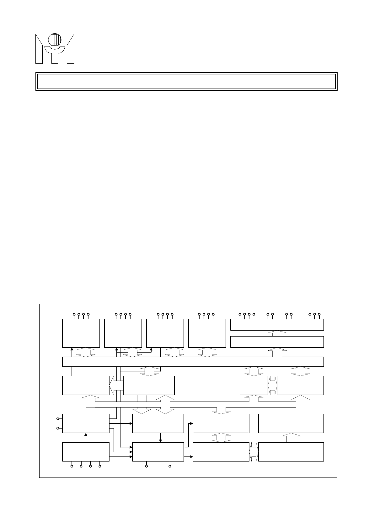
4-bit Microcontroller with LCD Driver
IOC 1~4
KEY SCAN
INPUT
SEG 31~33
RFC
SEG 29~30
EL-LIGHT
SEG 1~12
KEY SCAN
OUTPUT
LCD DRIVER
SEGMENT PLA
4 BITS DATA BUS
FREQUENCY
GENERATOR
ALU
DATA SRAM
(INDEX (L))
128 X 4 BITS
PREDIVIDER
6-BITS PRESET
TIMERX 2
8 LEVELS STACK
WATCHDOG
TIMER
OSCILLATOR
CONTROL
CIRCUIT
11-BIT PROGRAM
COUNTER
MASK ROM
2048 X 16 BITS
INSTRUCTION
DECODER
INDEX MASK
ROM
256 X 8 BITS
COM1~4 VDD1~3SEG1~33
........
INTPRESETCFOUT
CFIN
XTOUT
XTIN
CUP2
CUP1
This datasheet contains new product information. Myson Technology reserves the rights to modify the product specification without
notice. No liability is assumed as a result of the use of this procuts. No rights under any patent accompany the sales of the product.
BLOCK DIAGRAM
Page 2
MTU419B
(Preliminary)
MYSON
TECHNOLOGY
2/18 MTU419B Revision 3.0 28/Oct/1999
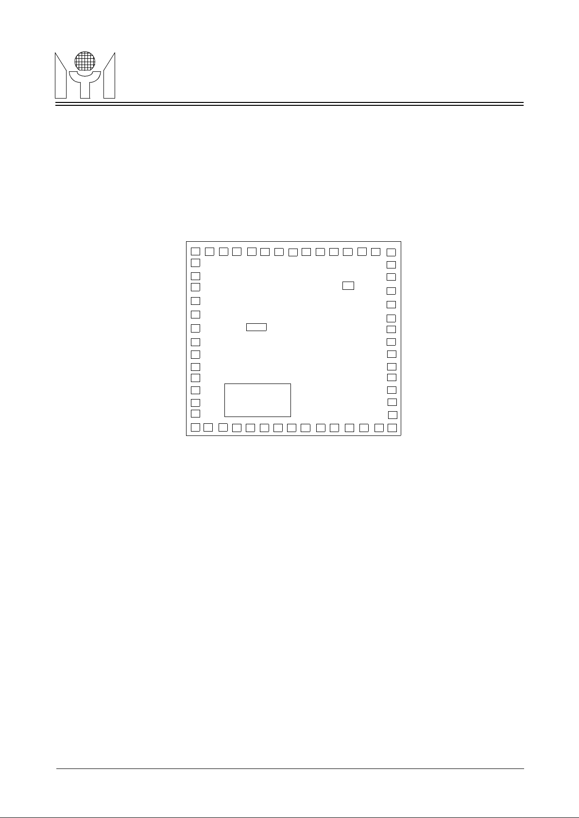
1.0 PAD DIAGRAM
Chip size : 1875 x 1875 µm
Pad size : 100 x 100 µm
Pad window : 90 x 90 µm
Pad pitch : min. 120 µm
IOC3 / KI3
IOC1 / KI1
XTOUT
XTIN
CFOUT
CFIN
BAK
VDD3
CUP1
CUP2
COM1
COM2
COM3
COM4
KO2 / SEG2
KO3 / SEG3
KO4 / SEG4
KO5 / SEG5
KO7 / SEG7
KO9 / SEG9
KO10 / SEG10
KO11 / SEG11
KO12 / SEG12
SEG13
SEG14
SEG15
SEG16
SEG17
SEG18
SEG19
SEG20
SEG21
SEG22
SEG23
SEG25
SEG26
SEG27
SEG28
SEG29 / ELC
SEG30 / ELP
SEG31 / RH
SEG32 / RT
SEG33 / RR
INT / CX
BZ
GND
KO6 / SEG6
KO8 / SEG8
SEG24
VDD1
IOC4 / KI4
IOC2 / KI2
RESET
TESTA
VDD2
ROM
LOGO
Code No.
KO1 / SEG1
Note: The substrate of die must connect to GND.
1
10
20
30 40
50
56
Page 3
MTU419B
(Preliminary)
MYSON
TECHNOLOGY
3/18 MTU419B Revision 3.0 28/Oct/1999
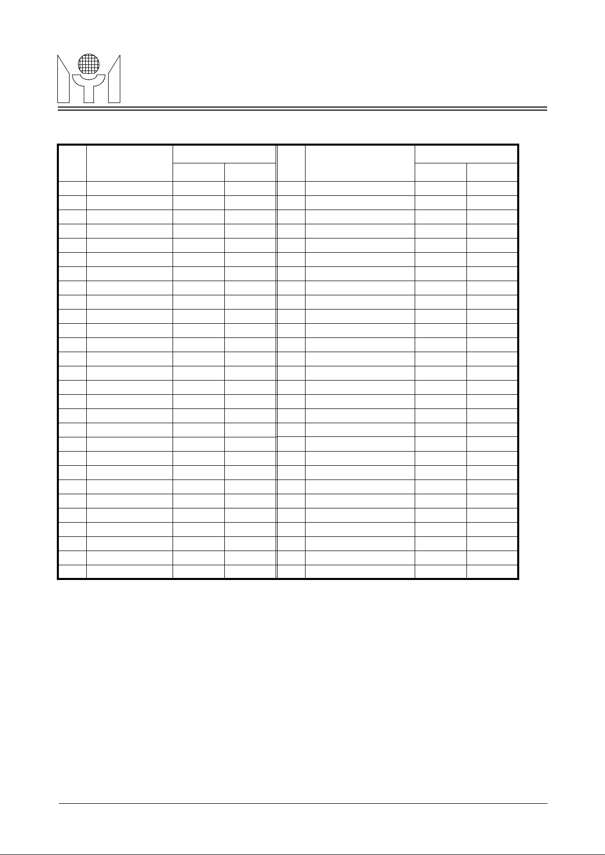
2.0 PAD ASSIGNMENT
Pad
No.
Pad Name
Coordinate
Pad
No.
Pad Name
Coordinate
X Y X Y
1 BAK 1657.5 1797.5 29 SEG9/KO9 217.5 77.5
2 CFIN 1537.5 1797.5 30 SEG10/KO10 337.5 77.5
3 CFOUT 1417.5 1797.5 31 SEG11/KO11 457.5 77.5
4 XTIN 1297.5 17975 32 SEG12/KO12 577.5 77.5
5 XTOUT 1177.5 1797.5 33 SEG13 697.5 77.5
6 TESTA 1057.5 1797.5 34 SEG14 817.5 77.5
7 RESET 937.5 1797.5 35 SEG15 937.5 77.5
8 IOC1/KI1 817.5 1797.5 36 SEG16 1057.5 77.5
9 IOC2/KI2 697.5 1797.5 37 SEG17 1177.5 77.5
10 IOC3/KI3 577.5 1797.5 38 SEG18 1297.5 77.5
11 IOC4/KI4 457.5 1797.5 39 SEG19 1417.5 77.5
12 VDD1 337.5 1797.5 40 SEG20 1537.5 77.5
13 VDD2 217.5 1797.5 41 SEG21 1657.5 77.5
14 VDD3 77.5 1797.5 42 SEG22 1797.5 77.5
15 CUP1 77.5 1657.5 43 SEG23 1797.5 217..5
16 CUP2 77.5 1537.5 44 SEG24 1797.5 337.5
17 COM1 77.5 1417.5 45 SEG25 1797.5 457.5
18 COM2 77.5 1297.5 46 SEG26 1797.5 577.5
19 COM3 77.5 1177.5 47 SEG27 1797.5 697.5
20 COM4 77.5 1057.5 48 SEG28 1797.5 817.5
21 SEG1/KO1 77.5 937.5 49 SEG29/ELC 1797.5 937.5
22 SEG2/KO2 77.5 817.5 50 SEG30/ELP 1797.5 1057.5
23 SEG3/KO3 77.5 697.5 51 SEG31/RH 1797.5 1177.5
24 SEG4/KO4 77.5 577.5 52 SEG32/RT 1797.5 1297.5
25 SEG5/KO5 77.5 457.5 53 SEG33/RR 1797.5 1417.5
26 SEG6/KO6 77.5 337.5 54 INT/CX 1797.5 1537.5
27 SEG7/KO7 77.5 217.5 55 BZ 1797.5 1657.5
28 SEG8/KO8 77.5 77.5 56 GND 1797.5 1797.5
Page 4
MTU419B
(Preliminary)
MYSON
TECHNOLOGY
4/18 MTU419B Revision 3.0 28/Oct/1999
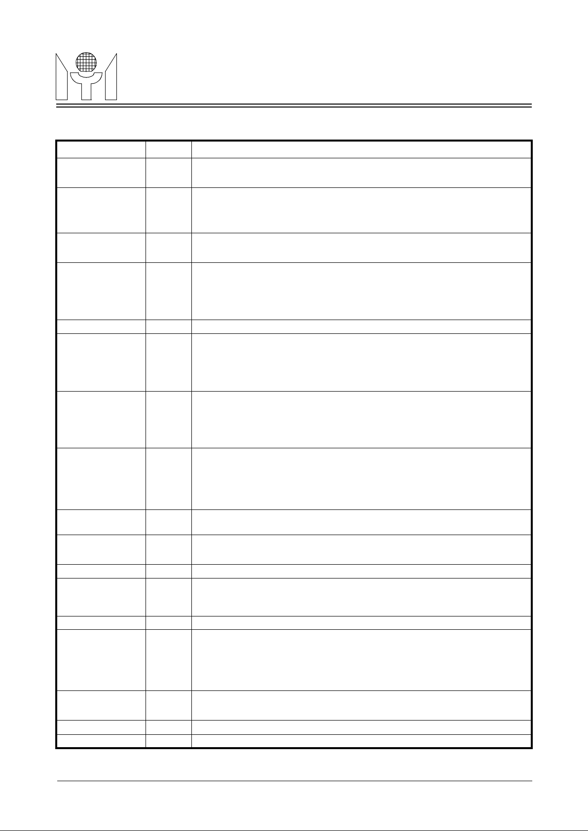
3.0 PAD DESCRIPTIONS
Name I/O Descriptions
BAK
Positive back-up voltage.
At Li mode, connects a 0.1u capacitance to GND.
VDD1,2,3
LCD drives voltage and positive supply voltage.
While Ag mode, connects +1.5V to VDD1.
While Li/ExtV mode, connects +3.0V to VDD2.
RESET I
Input pin from LSI reset request signal.
Internal pull-down resistor.
INT I
Input pin for external INT request signal.
Falling or rising edge triggered by mask option.
Internal pull-down or pull-up resistor or neither is selected by mask option
and shared with CX.
TESTA I Test signal input pin.
CUP1,2 O
Switching pins for supplying the LCD driving voltage to the VDD1, 2, 3 pins.
Connects the CUP1 and CUP2 pins with nonpolarized electrolytic capacitor if
1/2 or 1/3 bias mode has been selected.
In the static mode, these pins should be open.
XIN
XOUT
I
O
Time base counter frequency (clock specified, LCD alternating frequency,
alarm signal frequency) or system clock oscillation.
32KHz crystal oscillator.
Oscillation stops at the execution of stop instruction.
CFIN
CFOUT
I
O
System clock oscillation.
Connected with ceramic resonator.
Connected with RC oscillation circuit.
Oscillation stops at the execution of stop or slow instruction.
COM1,2,3,4 O
Output pins for supplying voltage to drive the common pins of the LCD or
LED panel.
SEG1-12 /
KO1~12
O
Output pins for LCD or LED panel segment.
Key strobe function, share pins as key scan output.
SEG13-33 O Output pins for LCD or LED panel segment.
IOC1-4 I/O
Input / Output port C, can use software to define internal pull-low / low-level
hold resistor and chattering clock to reduce input bounce and generate inter-
rupt.
KI1~4 I Key scan input, this port shares pins with IOC1~4 and is set by mask option.
RFC
CX
RR
RT
RH
I
O
O
O
1 input pin and 3 output pins for RFC application.
This port shares pins with SEG31~33 and INT, and is set by mask option.
EL
ELC
ELP
O
O
Output port for EL-light.
This port shares pins with SEG29,30, and is set by mask option.
ALM BZ O Output port for alarm, frequency or melody generator.
GND Negative supply voltage.
Page 5
MTU419B
(Preliminary)
MYSON
TECHNOLOGY
5/18 MTU419B Revision 3.0 28/Oct/1999
4.0 FUNCTIONAL DESCRIPTION
4.1 SRAM
The 128 X 4 bits SRAM is addressing by direct addressing or index addressing mode.
4.2 Index ROM
The 256 X 8 bits index ROM can be used in the 4-bit or 8-bit mode.
4.3 I/O Ports
The IOC port can be selected by software separately as input or output, and with/without internal pull-low and
different chattering clocks for halt release / interrupt trigger in order to reduce the input bounce for key scan:
PH6: 512Hz PH8: 128Hz PH10: 32Hz
The initial state of all IOC ports is input mode with pull-low.
Before setting the I/O ports from input to output, execute the output function first to ensure the output state.
4.4 Resistor to Frequency Converter
We use an RC oscillation circuit and a 16-bit counter to calculate the relative resistance of temperature and
humidity sensor. The diagram is shown below:
There are two kinds of methodology for measuring the input frequency: first, set FIN (i.e. CX) as the clock
input, using timer 2 or the software directly as interval control; second, if the FIN (CX) frequency is too low
(either because of a poor resolution for a fixed interval or a longer interval for better resolution but a longer
read-out rate [for example, 10 seconds per read-out]), you can switch the measure mode to set FIN (CX) as
interval control (it will enable the counter from the first FIN rising edge to the next rising edge, then will generate an interrupt) or use FREQ (internal frequency generator output) as clock input, hence you can count the
interval of CX.
To measure the resistor value of temperature and humidity sensor, first we measure the frequency of Rref,
then the frequency of Sensor:
Fref = K / Rref CX and
Fsensor = K / Rsensor CX, hence
Rsensor = Rref * Freq / Fsensor.
.
ELP
ENX
EHM
FIN
ERR
Timer
&
R/F Controller
16-Bit Counter
Freq
FreqCLCLLDLD
ENX
FIN
4-Bit Data Bus
RT
RH
RR
CX
RTP
RHM
Rref
CX
TMS
PH9
MRF
Where K is a coefficient for RC-oscillation and
will be a constant in a short time period.
Page 6
MTU419B
(Preliminary)
MYSON
TECHNOLOGY
6/18 MTU419B Revision 3.0 28/Oct/1999
4.5 Key_board Scanning Function
SEG1~12 shares the key_board scanning output, the output of the key_board scanning is a P open-drain to
VDDO (positive power supply) and all other SEGs and COMs are in Hi-z state during this period. This will minimize the effect of the LCD output.
The segment 1-12 also could be used as keyscan output and LCD still could be displayed with only slightly
affected.
SPK 00b5 b4 b3 b2 b1 b0.
b5: 1 will disable key-scan output.
b4: 1 will set all keyscan output as high, if b5=0.
b3~b0: will set the corresponding segment output as 1, if b5=0 and b4=0.
During power on, LCD off, STOP condition. All the common & segment output will be the chips supply power.
4.6 EL-light
Set ELC and ELP clock and duty cycle using ELC X instruction, then turn on and off ELC and ELP output by
SF X and RF X instruction. With external transistor, diode, inductor and resistor, we can pump the EL panel to
AC 100~250V.
When the EL-light is turned on, the ELC will turn on before ELP, but when the EL-light is off, the ELP and ELC
will turn off after the next falling edge of ELC in order to make sure no voltage is left on the EL plane.
4.7 TIMER
The 6-bit programmable timer can select PH3/PH9/PH15/FREQ (Timer 2 can also select PH5/ PH7/ PH11/
PH13 by TM2X instruction) as clock source. When it underflows, the halt release signals are generated.
4.8 Predivider
The predivider is a 15-sage counter that uses PH0 as clock source. The output of T-FF is changed when the
input signal is changed from H to L. PH11~15 are reset to L when PLC 100H instruction is executed or power
on reset or external reset is used. When PH14 is changed from H to L, the halt release signal is generated.
4.9 Alarm / Frequency / Melody
There is an 8-bit programmable counter and an 8-bit envelope control for alarm, frequency or melody output
from BZ/BZB.
The frequency counter can use software to select 1/2duty, 1/3duty,1/4duty drive modes.
LIT
ELP
ELC
L1
Q1
Q2
R1
R2
ELP
ELC
EL-plane
D1
Page 7

MTU419B
(Preliminary)
MYSON
TECHNOLOGY
7/18 MTU419B Revision 3.0 28/Oct/1999
4.10 INT Function
The INT pin can be selected by mask option as pull-high/pull-low or none and rising edge/falling edge trigger.
4.11 Watchdog Timer
The watchdog timer automatically generates a device reset when it overflows. The interval of overflow is 8/64/
512 x PH10 (set by mask option). You can use software to enable and disable this function. The watchdog
enable flag will be disabled by power on reset or reset pin reset condition, but can not be disabled by watchdog reset itself.
4.12 Halt Function
The halt instruction disables all clocks except predivider, timer, frequency counter, EL-light generator and
chattering clock to minimize the operating current.
4.13 Stop Function
The stop instruction disables all clocks to minimize the standby current, so only two external factors (INT, IOC
or key scan input) can release the stop condition.
FREQ
1/2 DUTY FREQ
1/3 DUTY FREQ
1/4 DUTY FREQ
Page 8

MTU419B
(Preliminary)
MYSON
TECHNOLOGY
8/18 MTU419B Revision 3.0 28/Oct/1999
5.0 BSOLUTE MAXIMUM RATINGS
at Ta = 0 to 70oC , GND = 0V
6.0 ALLOWABLE OPERATING CONDITIONS
at Ta = 0 to 70oC , GND = 0V
Name Symbol Range Unit
Maximum Supply Voltage
VDD1 -0.3 to 5.5 V
VDD2 -0.3 to 5.5 V
VDD3 -0.3 to 8.5 V
Maximum Input Voltage Vin -0.3 to VDD1/2+0.3 V
Maximum Output Voltage
Vout1 -0.3 to VDD1/2+0.3 V
Vout2 -0.3 to VDD3+0.3 V
Maximum Operating Temperature Topg 0 to +70
o
C
Maximum Storage Temperature Tstg -25 to +125
o
C
Name Symbol Condition Min. Max. Unit
Supply Voltage
VDD1 1.2 5.25 V
VDD2 2.4 5.25 V
VDD3 2.4 8.0 V
Oscillator Start-Up Voltage VDDB Crystal Mode 1.3 V
Oscillator Sustain Voltage VDDB Crystal Mode 1.2 V
Supply Voltage VDD1 Ag Mode 1.2 1.65 V
Supply Voltage VDD2 EXT-V , Li Mode 2.4 5.25 V
Input "H" Voltage Vih1 Ag Battery Mode VDD1 - 0.7 VDD1 + 0.7 V
Input "L" Voltage Vil1
Li Battery Mode
- 0.7 0.7 V
Input "H" Voltage Vih2 VDD2 - 0.7 VDD2 + 0.7 V
Input "L" Voltage Vil2 - 0.7 0.7 V
Input "H" Voltage Vih3
OSCIN at Ag Battery Mode
0.8 x VDD1 VDD1 V
Input "L" Voltage Vil3 0 0.2 x VDD1 V
Input "H" Voltage Vih4
OSCIN at Li Battery Mode
0.8 x VDD2 VDD2 V
Input "L" Voltage Vil4 0 0.2 x VDD2 V
Input "H" Voltage Vih5
CFIN at Li Battery or EXT-V
Mode
0.8 x VDD2 VDD2 V
Input "L" Voltage Vil5 0 0.2 x VDD2 V
Input "H" Voltage Vih6
RC Mode
0.8 x VDDO VDDO V
Input "L" Voltage Vil6 0 0.2 x VDDO V
Operating Freq
Fopg1 Crystal Mode 32 3580 KHz
Fopg2 External RC Mode 32 1000 KHz
Fopg3 CF Mode 1000 3580 KHz
Page 9

MTU419B
(Preliminary)
MYSON
TECHNOLOGY
9/18 MTU419B Revision 3.0 28/Oct/1999
7.0 ELECTRICAL CHARACTERICTICS
7.1 Input Resistance
at #1 : VDD1 = 1.2V ( Ag )
7.2 DC Output Characteristics
at #2 : VDD2 = 2.4V ( Li )
Name Symbol Condition Min. Typ. Max. Unit
"L" Level Hold Tr (IOC)
Rllh1 Vi = 0.2VDD1 , #1 10 40 100 Kohm
Rllh2 Vi = 0.2VDD2 , #2 10 40 100 Kohm
Rllh3 Vi = 0.2VDD2 , #3 5 20 50 Kohm
IOC Pull-Down Tr
Rmad1 Vi = VDD1 , #1 200 500 1000 Kohm
Rmad2 Vi = VDD2 , #2 200 500 1000 Kohm
Rmad3 Vi = VDD3 , #3 100 250 500 Kohm
INT Pull-up Tr
Rintu1 Vi = VDD1 , #1 200 500 1000 Kohm
Rintu2 Vi = VDD2 , #2 200 500 1000 Kohm
Rintu3 Vi = VDD3 , #3 100 250 500 Kohm
INT Pull-Down Tr
Rintd1 Vi = GND , #1 200 500 1000 Kohm
Rintd2 Vi = GND , #2 200 500 1000 Kohm
Rintd3 Vi = GND , #3 100 250 500 Kohm
RES Pull-Down R
Rres1 Vi = GND or VDD1 , #1 5 20 50 Kohm
Rres2 Vi = GND or VDD2 , #2 5 20 50 Kohm
Rres3 Vi = GND or VDD2 , #3 5 20 50 Kohm
Name Symbol Condition Port Min. Typ. Max. Unit
Output "H" Voltage
Voh1a Ioh = -10uA, #1
SEG1~33
0.8 0.9 1.0 V
Voh2a Ioh = -50uA, #2 1.5 1.8 2.1 V
Voh3a Ioh = -200uA, #3 2.5 3 3.5 V
Output "L" Voltage
Vol1a Iol = 20uA, #1 0.2 0.3 0.4 V
Vol2a Iol = 100uA, #2 0.3 0.6 0.9 V
Vol3a Iol = 400uA, #3 0.5 1 1.5 V
Output "H" Voltage
Voh1c Ioh = -200uA, #1
IOC-n
0.8 0.9 1.0 V
Voh2c Ioh = -1mA, #2 1.5 1.8 2.1 V
Voh3c Ioh = -3mA, #3 2.5 3 3.5 V
Output "L" Voltage
Vol1c Iol = 400uA,#1 0.2 0.3 0.4 V
Vol2c Iol = 2mA, #2 0.3 0.6 0.9 V
Vol3c Iol = 6mA, #3 0.5 1 1.5 V
Page 10

MTU419B
(Preliminary)
MYSON
TECHNOLOGY
10/18 MTU419B Revision 3.0 28/Oct/1999
7.3 Segment Driver Output Characteristic
at #3 : VDD2 = 4V ( Ext-V )
Name Symb. Condition For Min. Typ. Max. Unit
Static Display Mode
Output 'H' Voltage
Voh1d Ioh=-1uA, #1
SEG-n
1.0 V
Voh2d Ioh=-1uA, #2 2.2 V
Voh3d Ioh=-1uA, #3 3.8 V
Output 'L' Voltage
Vol1d Iol=1uA, #1 0.2 V
Vol2d Iol=1uA, #2 0.2 V
Vol3d Iol=1uA, #1 0.2 V
Output 'H' Voltage
Voh1e Ioh=-10uA, #1
COM-n
1.0 V
Voh2e Ioh=-10uA, #2 2.2 V
Voh3e Ioh=-10uA, #3 3.8 V
Output 'L' Voltage
Vol1e Ioh=10uA, #1 0.2 V
Vol2e Ioh=10uA, #2 0.2 V
Vol3e Ioh=10uA, #3 0.2 V
1/2 Bias Display Mode
Output 'H' Voltage
Voh12f Ioh=-1uA, #1, #2
SEG-n
2.2 V
Voh3f Ioh=-1uA, #3 3.8 V
Output 'L' Voltage
Vol12f Iol=1uA, #1, #2 0.2 V
Vol3f lol=1uA, #3 0.2 V
Output 'H' Voltage
Voh12g Ioh=-10uA, #1, #2
COM-n
2.2 V
Voh3g Ioh=-10uA, #3 3.8 V
Output 'M' Voltage
Vom12g Iol/h=+/-10uA, #1, #2 1.0 1.4 V
Vom3g Iol/h=+/-10uA, #3 1.8 2.2 V
Output 'L' Voltage
Vol12g lol=10uA, #1, #2 0.2 V
Vol3g lol=10uA, #3 0.2 V
1/3 Bias Display Mode
Output 'H' Voltage
Voh12i loh=-1uA, #1, #2
SEG-n
3.4 V
Voh3i loh=-1uA, #3 5.8 V
Output 'M1' Voltage
Vom12i lol/h=+/-10uA, #1, #2 1.0 1.4 V
Vom13i lol/h=+/-10uA, #3 1.8 2.2 V
Output 'M2' Voltage
Vom22i lol/h=+/-10uA, #1, #2 2.2 2.6 V
Vom23i lol/h=+/-10uA, #3 3.8 4.2 V
Output 'L' Voltage
Vol12i lol=1uA, #1, #2 0.2 V
Vol3i lol=1uA, #3 0.2 V
Output 'H' Voltage
Voh12j loh=-10uA, #1, #2
COM-n
3.4 V
Voh3j loh=-10uA, #3 5.8 V
Output 'M1' Voltage
Vom12j lol/h=+/-10uA, #1, #2 1.0 1.4 V
Vom13j lol/h=+/-10uA, #3 1.8 2.2 V
Output 'M2' Voltage
Vom22j lol/h=+/-10uA, #1, #2 2.2 2.6 V
Vom23j lol/h=+/-10uA, #3 3.8 4.2 V
Output 'L' Voltage
Vol12j loh=10uA, #1, #2 0.2 V
Vol3j loh=10uA, #3 0.2 V
Page 11

MTU419B
(Preliminary)
MYSON
TECHNOLOGY
11/18 MTU419B Revision 3.0 28/Oct/1999
8.0 INSTRUCTION TABLE ( Total 135 instructions )
Instruction Machine Code Functions Flag/Remark
NOP 0000 0000 0000 0000 No Operation
LCT Lz, Ry 0000 001Z ZZZZ YYYY Lz ⇐ { 7SEG ⇐ Ry}
LCB Lz, Ry 0000 010Z ZZZZ YYYY Lz ⇐ { 7SEG ⇐ Ry}
LCP Lz, Ry 0000 011Z ZZZZ YYYY Lz ⇐ Ry , AC
LCD Lz, @HL 0000 100Z ZZZZ 0000 Lz ⇐ T@HL
OPC Rx 0000 1101 0XXX XXXX Port(C) ⇐ Rx
FRQ Rx, D 0001 00DD 0XXX XXXX
FREQ
DD=00
DD=01
DD=10
⇐ Rx, AC
: 1/4 Duty
: 1/3 Duty
: 1/2 Duty
FRQ D,@HL 0001 01DD 0000 0000 FREQ ⇐ T@HL
FRQX D,X 0001 10DD XXXX XXXX FREQ ⇐ X
MVL Rx 0001 1100 0XXX XXXX L ⇐ Rx
MVH Rx 0001 1101 0XXX XXXX H ⇐ Rx
ADC Rx 0010 0000 0XXX XXXX AC ⇐ Rx+AC+CF CF
ADC @HL 0010 0000 1000 0000 AC ⇐ @HL+AC+CF CF
ADC* Rx 0010 0001 0XXX XXXX AC, Rx ⇐ Rx+AC+CF CF
ADC* @HL 0010 0001 1000 0000 AC, @HL ⇐ @HL+AC+CF CF
SBC Rx 0010 0010 0XXX XXXX AC ⇐ Rx+ACB+CF CF
SBC @HL 0010 0010 1000 0000 AC ⇐ @HL+ACB+CF CF
SBC* Rx 0010 0011 0XXX XXXX AC, Rx ⇐ Rx+ACB+CF CF
SBC* @HL 0010 0011 1000 0000 AC, @HL ⇐ @HL+ACB+CF CF
ADD Rx 0010 0100 0XXX XXXX AC ⇐ Rx+AC CF
ADD @HL 0010 0100 1000 0000 AC ⇐ @HL+AC CF
ADD* Rx 0010 0101 0XXX XXXX AC, Rx ⇐ Rx+AC CF
ADD* @HL 0010 0101 1000 0000 AC, @HL ⇐ @HL+AC CF
SUB Rx 0010 0110 0XXX XXXX AC ⇐ Rx+ACB+1 CF
SUB @HL 0010 0110 1000 0000 AC ⇐ @HL+ACB+1 CF
SUB* Rx 0010 0111 0XXX XXXX AC, Rx ⇐ Rx+ACB+1 CF
SUB* @HL 0010 0111 1000 0000 AC,@HL ⇐ @HL+ACB+1 CF
ADN Rx 0010 1000 0XXX XXXX AC ⇐ Rx+AC
ADN @HL 0010 1000 1000 0000 AC ⇐ @HL+AC
ADN* Rx 0010 1001 0XXX XXXX AC, Rx ⇐ Rx+AC
ADN* @HL 0010 1001 1000 0000 AC,@HL ⇐ @HL+AC
AND Rx 0010 1010 0XXX XXXX AC ⇐ Rx AND AC
AND @HL 0010 1010 1000 0000 AC ⇐ @HL AND AC
AND* Rx 0010 1011 0XXX XXXX AC, Rx ⇐ Rx AND AC
AND* @HL 0010 1011 1000 0000 AC,@HL ⇐ @HL AND AC
EOR Rx 0010 1100 0XXX XXXX AC ⇐ Rx EXOR AC
EOR @HL 0010 1100 1000 0000 AC ⇐ @HL EXOR AC
EOR* Rx 0010 1101 0XXX XXXX AC, Rx ⇐ Rx EXOR AC
EOR* @HL 0010 1101 1000 0000 AC,@HL ⇐ @HL EXOR AC
OR Rx 0010 1110 0XXX XXXX AC ⇐ Rx OR AC
OR @HL 0010 1110 1000 0000 AC ⇐ @HL OR AC
OR* Rx 0010 1111 0XXX XXXX AC, Rx ⇐ Rx OR AC
Page 12

MTU419B
(Preliminary)
MYSON
TECHNOLOGY
12/18 MTU419B Revision 3.0 28/Oct/1999
OR* @HL 0010 1111 1000 0000 AC,@HL ⇐ @HL OR AC
ADCI Ry,D 0011 0000 DDDD YYYY AC ⇐ Ry+D+CF CF
ADCI* Ry,D 0011 0001 DDDD YYYY AC, Ry ⇐ Ry+D+CF CF
SBCI Ry,D 0011 0010 DDDD YYYY AC ⇐ Ry+DB+CF CF
SBCI* Ry,D 0011 0011 DDDD YYYY AC, Ry ⇐ Ry+DB+CF CF
ADDI Ry,D 0011 0100 DDDD YYYY AC ⇐ Ry+D CF
ADDI* Ry,D 0011 0101 DDDD YYYY AC, Ry ⇐ Ry+D CF
SUBI Ry,D 0011 0110 DDDD YYYY AC ⇐ Ry+DB+1 CF
SUBI* Ry,D 0011 0111 DDDD YYYY AC, Ry ⇐ Ry+DB+1 CF
ADNI Ry,D 0011 1000 DDDD YYYY AC ⇐ Ry+D
ADNI* Ry,D 0011 1001 DDDD YYYY AC, Ry ⇐ Ry+D
ANDI Ry,D 0011 1010 DDDD YYYY AC ⇐ Ry AND D
ANDI* Ry,D 0011 1011 DDDD YYYY AC, Ry ⇐ Ry AND D
EORI Ry,D 0011 1100 DDDD YYYY AC ⇐ Ry EXOR D
EORI* Ry,D 0011 1101 DDDD YYYY AC, Ry ⇐ Ry EXOR D
ORI Ry,D 0011 1110 DDDD YYYY AC ⇐ Ry OR D
ORI* Ry,D 0011 1111 DDDD YYYY AC, Ry ⇐ Ry OR D
INC* Rx 0100 0000 0XXX XXXX AC, Rx ⇐ Rx+1
INC* @HL 0100 0000 1000 0000 AC, @HL ⇐ @HL+1
DEC Rx 0100 0001 0XXX XXXX AC, Rx ⇐ Rx-1
DEC* @HL 0100 0001 1000 0000 AC, @HL ⇐ @HL-1
IPC Rx 0100 0111 0XXX XXXX AC, Rx ⇐ Port(C)
MAF Rx 0100 1010 0XXX XXXX AC,Rx ⇐ STS1
B3 : CF
B2 : AC=0
B1 : (No use)
B0 : (No use)
MSB Rx 0100 1011 0XXX XXXX AC,Rx ⇐ STS2
B3 : (No use)
B2 : SCF2(HRx)
B1 : SCF1(CPT)
B0 : BCF
MSC Rx 0100 1100 0XXX XXXX AC,Rx ⇐ STS3
B3 : SCF7(PDV)
B2 : PH15
B1 :
SCF5(TMR1)
B0 : SCF4(INT)
MCX Rx 0100 1101 0XXX XXXX AC,Rx ⇐ STS3X
B3 :SCF9(RFC)
B2: (no use)
B1 :SCF6(TMR2)
B0 :(No use)
MSD Rx 0100 1110 0XXX XXXX AC,Rx ⇐ STS4
B3 : (No use)
B2 : RFOVF
B1 : WDF
B0 : CSF
SR0 Rx 0101 0000 0XXX XXXX
ACn, Rxn
AC3, Rx3
⇐ Rx(n+1)
⇐ 0
SR1 Rx 0101 0001 0XXX XXXX
ACn, Rxn
AC3, Rx3
⇐ Rx(n+1)
⇐ 1
SL0 Rx 0101 0010 0XXX XXXX
ACn, Rxn
AC0, Rx0
⇐ Rx(n-1)
⇐ 0
Instruction Machine Code Functions Flag/Remark
Page 13

MTU419B
(Preliminary)
MYSON
TECHNOLOGY
13/18 MTU419B Revision 3.0 28/Oct/1999
SL1 Rx 0101 0011 0XXX XXXX
Can, Rxn
AC0, Rx0
⇐ Rx(n-1)
⇐ 1
DAA 0101 0100 0000 0000 AC ⇐ BCD(AC)
DAA* Rx 0101 0101 0XXX XXXX AC, Rx ⇐ BCD(AC)
DAA* @HL 0101 0101 1000 0000 AC, @HL ⇐ BCD(AC)
DAS 0101 0110 0000 0000 AC ⇐ BCD(AC)
DAS* Rx 0101 0111 0XXX XXXX AC, Rx ⇐ BCD(AC)
DAS* @HL 0101 0111 1000 0000 AC, @HL ⇐ BCD(AC)
LDS Rx,D 0101 1DDD DXXX XXXX AC, Rx ⇐ D
LDH Rx,@HL 0110 0000 0XXX XXXX AC, Rx ⇐ H(T@HL)
LDH* Rx,@HL 0110 0001 0XXX XXXX
AC, Rx
HL
⇐ H(T@HL)
⇐ HL + 1
LDL Rx,@HL 0110 0010 0XXX XXXX AC, Rx ⇐ L(T@HL)
LDL* Rx,@HL 0110 0011 0XXX XXXX
AC, Rx
HL
⇐ L(T@HL)
⇐ @HL + 1
MRF1 Rx 0110 0100 0XXX XXXX AC,Rx ⇐ RFC3-0
MRF2 Rx 0110 0101 0XXX XXXX AC,Rx ⇐ RFC7-4
MRF3 Rx 0110 0110 0XXX XXXX AC,Rx ⇐ RFC11-8
MRF4 Rx 0110 0111 0XXX XXXX AC,Rx ⇐ RFC15-12
STA Rx 0110 1000 0XXX XXXX Rx ⇐ AC
STA @HL 0110 1000 1000 0000 @HL ⇐ AC
LDA Rx 0110 1100 0XXX XXXX AC ⇐ Rx
LDA @HL 0100 1100 1000 0000 AC ⇐ @HL
MRA Rx 0110 1101 0XXX XXXX CF ⇐ Rx3 CF
MRW @HL,Rx 0110 1110 0XXX XXXX AC,@HL ⇐ Rx
MWR Rx,@HL 0110 1111 0XXX XXXX AC,Rx ⇐ @HL
MRW Ry,Rx 0111 0YYY YXXX XXXX AC,Ry ⇐ Rx
MWR Rx,Ry 0111 1YYY YXXX XXXX AC,Rx ⇐ Ry
JB0 X 1000 0XXX XXXX XXXX PC ⇐ X if AC0 = 1
JB1 X 1000 1XXX XXXX XXXX PC ⇐ X if AC1 = 1
JB2 X 1001 0XXX XXXX XXXX PC ⇐ X if AC2 = 1
JB3 X 1001 1XXX XXXX XXXX PC ⇐ X if AC3 = 1
JNZ X 1010 0XXX XXXX XXXX PC ⇐ X if AC ≠ 0
JNC X 1010 1XXX XXXX XXXX PC ⇐ X if CF = 0
JZ X 1011 0XXX XXXX XXXX PC ⇐ X if AC = 0
JC X 1011 1XXX XXXX XXXX PC ⇐ X if CF = 1
CALL X 1100 0XXX XXXX XXXX
STACK
PC
⇐ PC+1
⇐ X
JMP X 1101 0XXX XXXX XXXX PC ⇐ X
RTS 1101 1000 0000 0000 PC ⇐ STACK CALL Return
SCC X 1101 1001 0X0X 0XXX
X6 = 1
X6 = 0
X4 = 0
X2,1,0=001
X2,1,0=010
X2,1,0=100
: Cfq = BCLK
: Cfq = PH0
: Set P(C)
: Cch = PH10
: Cch = PH8
: Cch = PH6
SCA X 1101 1010 000X 0000 X4 : C1-4 Enable (SEF4)
Instruction Machine Code Functions Flag/Remark
Page 14

MTU419B
(Preliminary)
MYSON
TECHNOLOGY
14/18 MTU419B Revision 3.0 28/Oct/1999
SPC X 1101 1110 000X XXXX
X4
X3~0
: Set C4-1 Pull-Low
/ Low-Level-Hold
: Set C4-1 I/O
SPK Rx 1100 0011 00XX XXXX
X5=1
X4=1
X3~0
: Set all Hi-z
: Set all 1
: Set n of 12
SPKI X 0000 101X 0000 0000
X8=0
X8=1
: Set HRF5 from port C
/ key scan input
: Set HRF5 from key
strobe signal
IPI Rx 0100 0010 1XXX XXXX [Rx] AC ⇐ 11160 HRF5 control bit
TMS Rx 1110 0000 0XXX XXXX Timer1 ⇐ Rx, AC
TMS @HL 1110 0001 0000 0000 Timer1 ⇐ T@HL
TMSX X 1110 0010 XXXX XXXX
X7,6 = 11
X7,6 = 10
X7,6 = 01
X7,6 = 00
X5~0
: Ctm = FREQ
: Ctm = PH15
: Ctm = PH3
: Ctm = PH9
: Set Timer1 Value
TM2 Rx 1110 0100 0XXX XXXX Timer2 ⇐ Rx, AC
TM2 @HL 1110 0101 0000 0000 Timer2 ⇐ T@HL
TM2X X 1110 011X XXXX XXXX
X8,7,6=111
X8,7,6=110
X8,7,6=101
X8,7,6=000
X8,7,6=011
X8,7,6=010
X8,7,6=001
X8,7,6=000
X5~0
: Ctm = PH13
: Ctm = PH11
: Ctm = PH7
: Ctm = PH5
: Ctm = FREQ
: Ctm = PH15
: Ctm = PH3
: Ctm = PH9
: Set Timer2 Value
SHE X 1110 1000 0XXX XXX0
X6
X5
X4
X3
X2
X1
: Enable HEF6(RFC)
: Enable HEF5(KEY)
: Enable HEF4(TMR2)
: Enable HEF3(PDV)
: Enable HEF2(INT)
: Enable HEF1(TMR1)
SIE* X 1110 1001 0XXX XXXX
X6
X5
X4
X3
X2
X1
X0
: Enable IEF6(RFC)
: Enable IEF5(KEY)
: Enable IEF4(TMR2)
: Enable IEF3(PDV)
: Enable IEF2(INT)
: Enable IEF1(TMR1)
: Enable IEF0(A,CPT)
PLC X 1110 101X 0XXX XXXX
X8
X6~0
: Reset PH15~11
: Reset HRF6~0
SRF X 1110 1100 00XX XXXX
X5
X4
X3
X2
X1
X0
: Enable Cx Control
: Enable Timer2 Control
: Enable Counter
: Enable RH Output
: Enable RT Output
: Enable RR Output
ENX
EHM
ETP
ERR
Instruction Machine Code Functions Flag/Remark
Page 15

MTU419B
(Preliminary)
MYSON
TECHNOLOGY
15/18 MTU419B Revision 3.0 28/Oct/1999
SRE X 1110 1101 X0XX 0000 X6~4 : Enable SRF7,5-4
SRF7 (KEY)
SRF5 (HRF2)
SRF4 (M Port)
FAST 1110 1110 0000 0000 SCLK : High Speed Clock
SLOW 1110 1111 0000 0000 SCLK : Low Speed Clock
SF X 1111 0000 X00X XXXX
X7
X4
X3
X2
X1
X0
: Reload Set
: WDT Enable
: HALT after EL LIGHT
: EL LIGHT On
: BCF Set
: CF Set
RL1
WDF
BCF
CF
RF X 1111 0100 X00X 0XXX
X7
X4
X2
X1
X0
: Reload Reset
: WDT Reset
: EL LIGHT Off
: BCF Reset
: CF Reset
RL1
WDF
BCF
CF
SF2 X 1111 1000 0000 0XXXX0X1
X2
: Reload Set
: Dis-ENX Set
: Close all segments
RL2
DED
RSOFF
RF2 X 1111 1001 0000 0XXXX0X1
X2
: Reload Reset
: Dis-ENX Reset
: Release all Segments
RL2
DED
RSOFF
ALM X 1111 101X XXXX XXXX
X8,7,6=111
X8,7,6=100
X8,7,6=011
X8,7,6=010
X8,7,6=001
X8,7,6=000
X5~0
: FREQ
: DC1
: PH3
: PH4
: PH5
: DC0
⇐ PH15~10
ELC X 1111 110X XXXX XXXX
X8=1
X8=0
X7,6=11
X7,6=10
X7,6=01
X7,6=00
X5,4=11
X5,4=10
X5,4=01
X5,4=00
X3,2=11
X3,2=10
X3,2=01
X3,2=00
X1,0=11
X1,0=10
X1,0=01
X1,0=00
BCLKX
PH0
BCLK/8
BCLK/4
BCLK/2
BCLK
1/1
1/2
1/3
1/4
PH5
PH6
PH7
PH8
1/1
1/2
1/3
1/4
ELP - CLK
BCLKX
ELP - DUTY
ELC - CLK
ELC - DUTY
HALT 1111 1110 0000 0000 Halt Operation
STOP 1111 1111 0000 0000 Stop Operation
Instruction Machine Code Functions Flag/Remark
Page 16

MTU419B
(Preliminary)
MYSON
TECHNOLOGY
16/18 MTU419B Revision 3.0 28/Oct/1999
8.1 Symbol Description
AC : Accumulator D : Immediate data
ACn : Accumulator bit-n PC : Program counter
X : Address CF : Carry flag
Rx : Memory of address X Rxn : Memory bit-n of address X
WDF : Watchdog timer enable flag Ry : Memory of working register Y
HL : Index register BCF : Back-up flag
BCLK : System clock address @HL : Memory of index RAM
IEFn : Interrupt enable flag HRFn : Halt release flag
SRFn : Stop release enable flag HEFn : Halt release enable flag
SCFn : Start condition flag Cfq : Clock source of frequency generator
Cch : Clock source of chartering detector Ctm : Clock source of timer
TMR : Timer overflow release flag PDV : Predivider
SEFn : Switch enable flag Lz : LCD latch
FREQ : Frequency generator setting value T@HL : Memory of index ROM
ADF : ADC flag CSF : Clock source flag
DAC : Digital-to-analog converter output signal
LBR : Low-battery voltage reference L : Low address of index
H : High address of index RFOVF : RFC overflow flag
HT@HL : High nibble of index ROM LT@HL : Low nibble of index ROM
Page 17

MTU419B
(Preliminary)
MYSON
TECHNOLOGY
17/18 MTU419B Revision 3.0 28/Oct/1999
9.0 APPENDIX ( Important Issue for MTU419/419B/428/429B )
9.1 Chip’s internal vlotage V.S. power mode and external connection
Note *1: VDD3 is only used for LCD operating in 1/3 bias and 1/4 bias. If 1/2 bias chosen, VDD3 need be
connected to VDD2 (VDD3 is equal to VDD2).
*2: VDD4 is only used for LCD operating in 1/4 bias. If 1/3 bias chosen, VDD4 need be connected to
VDD3 (VDD4 is equal to VDD3). If 1/2 bias chosen, VDD4 need be connected to VDD2 (VDD4 is
equal to VDD2).
*3: BAK is defined as chip’s internal power supply node, which is used only for internal logic circuitry.
A. Whatever the power mode used, all external VDD# pins must connect a capacitor (0.05uF or 0.1uF) to
GND for decoupling power noise using.
B. All VDD# pins other than Vsupply are from voltage charge pump, i.e. If no clock, then VDD# pins can not
supply out.
C. Vsupply is the power supply for Chip and depends on the power mode used, all the input and output pins
voltage range follow the Vsupply.
9.2 The capacitor connected between CUP2 and CUP3 is only when MTU429B operating in 1/4 bias.
9.3 Some notes for BCF flag
BCF is always set to “High” automatically after Power on, Reset and Stop mode.
A. For power saving use, BCF may be set to “Low” which can reduce chip’s current consumption.
B. Ag and Li battery mode applications:
After Power on, Reset or release from Stop mode. Need to wait 2 seconds long, then can set BCF to
“Low”.
C. Larger current load and fast clock:
a. BCF should be set to “High” for the case of fast clock or larger current load (such as RFC, ADC, DAC,
EL-light and Buzzer output) use.
b. After set BCF to “high”, need wait 2 ms long at least, then can enable larger current load. Or after
disable Larger current load, need wait 2ms long at least, then can set BCF to “Low”
D. Li battery mode applications:
Especially for Li battery mode, BCF switching will cause a temporary current surge (or power noise)
on BAK. Furthermore if not necessary, don’t switch BCF too often as possible.
E. Improperly use of BCF will cause malfunction to chips.
AG LI EXT-V
VDD1 Vsupply 1/2 x Vsupply 1/2 x Vsupply
VDD2 2 x VDD1 Vsupply Vsupply
VDD3 *1 3 x VDD1 3/2 x Vsupply 3/2 x Vsupply
VDD4 *2 4 x VDD1 2 x Vsupply 2 x Vsupply
BAK *3 VDD1 BCF = 0 BCF=1 VDD2
VDD1 VDD2
Page 18

MTU419B
(Preliminary)
MYSON
TECHNOLOGY
18/18 MTU419B Revision 3.0 28/Oct/1999
F. Lower current consumption and reliability:
The chip’s reliability will greatly decrease if invalid use BCF, especially for Li-battery mode. Because the
chip’s internal power also switches between VDD1 and VDD2, which also cause a temporary power
noise.
9.4 Input pin
Any input pins floating will cause chips in malfunction and large current consumption.
9.5 32.768KHz X’tal oscillator
Always layout the X’tal as close the Chips as possible and don’t place any signals across the layout routing.
Since X’tal oscillation circuit consumes current only 0.5uA to 1uA, any power noise will disturb the oscillation.
The proper external capacitors for Xin and Xout are necessary for the accuracy and stability of oscillation.
1/( Cin+Cpcb ) + 1/( Cout+Cpcb ) = 1/CL
The Chip’s Xout pin has an internal capacitor around 10~20pf connected to BAK (chip’s internal Node).
For example
Epson’s C-001R 20ppm, CL=12.5pf
Cin = 25pf
Cout = 15pf
The time accuracy will be around +/- 0.5 second/day
Note: The parasitic capacitors of X’tal pins in PCB layout need be considered in above calculation.
9.6 RFC / Event counter / IOA for MTU429B
If anyone uses RFC / Event counter function and IOAs in the same application, make sure the pin IOA1
(which is corresponding to CX by mask option) must set as IOA’s output mode by SPA instruction. Or the
signal changes on CX pin may cause halt release or interrupt for IOA’s port. In this case the program couldn’t
function properly.
Myson Technology, Inc.
No. 2, Industry E. Rd. III, Science-Based Industrial Park, Hsinchu, Taiwan, R. O. C.
Tel: +886-3-5784866 Fax: +886-3-5785002 http://www.myson.com.tw
 Loading...