

Page 1

MYSON
TECHNOLOGY
MTU410
4-Bit Micro-Controller with LCD Driver, 1K Word
FEATURES
• Very low current dissipation.
• Wide operating voltage range.
• Supports both Ag and Li batteries.
• Powerful instruction set.
• 4-level subroutine nesting (including interrupt).
• 4 event driven interrupts, 2 external and 2 internal.
• ROM size: 1024 x 15 bits.
• RAM size: 64 x 4 bits.
• Input ports: 2 ports/ 8 pins (S and M).
• Output port: 1 port/ 4 pins (P).
• Pseudo serial output port (P).
• Input/output ports: 2 ports/ 8 pins (I/OA and I/OB).
• Control outputs: ALARM, LIGHT.
• LCD driver outputs (can drive up to 75 LCD segments).
• Mask option to select 4 LCD drive modes: static, duplex (1/2 duty 1/2 bias, 1/3 duty 1/2 bias
or 1/3 duty 1/3 bias).
• Mask option permits LCD driver output pins to be used for DC output ports; up to 25 pins are available.
• Segment PLA circuit permits any layout on LCD panel.
• Built-in clock generator (crystal or RC).
• Built-in voltage doubler, halver, tripler.
GENERAL DESCRIPTION
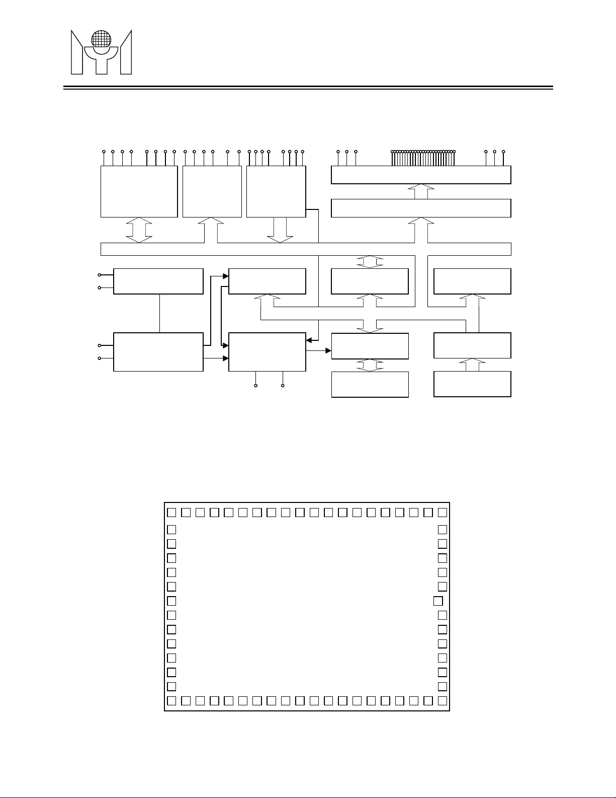
The MTU410 is a single chip 4-bit microcontroller with LCD drivers. It can drive up to 3 common times or 25
segments, i.e. a 75-segment LCD driver. This 4-bit microcontroller contains a 4-bit parallel processing ALU,
1024 x 15-bit program ROM, 64 x 4-bit data RAM, input/output ports, alarm driver, timer, clock generator,
crystal and RC oscillator circuit, LCD driver and 79 powerful instructions in a single chip. The HALT instruction
can be used to stop all internal operations other than timer, clock generator, crystal/RC oscillator and LCD
driver. Very low current dissipation can be easily achieved by combining 4 kinds of interrupt functions and HALT
instruction to minimize the operation cycle.
This datasheet contains new product information. Myson Technology reserves the rights to modify the product specification without notice.
No liability is assumed as a result of the use of this product. No rights under any pat ent accompany the sale of the produc t .
1/10
MTU410 Revision 2.7 04/28/1998
Page 2
MYSON
TECHNOLOGY
BLOCK DIAGRAM
I/O
A1~4
BIDIRECTION
I/O PORT
OSC
IN
OSC
OUT
CUP 1
CUP 2
I/O
B1~4
OSCILLATOR
PREDIVIDER
P1~4
OUTPUT
PORT
ALARM
S1~4
LIGHT
6-BIT PRESET
TIMER
CONTROL
CIRCUIT
INPUT
PORT
4-BIT DATA BUS
COM 1~3M1~4
ALU
10-BIT PROGRAM
COUNTER
SEG1~25
LCD DRIVER
SEGMENT PLA
RAM 64 X 4 BITS
INSTRUCTION
MTU410
VSS1~3
DECODER
RESET
1.0 PACKAGE & CHIP INFORMATION
Chip size 3245um X 2325um
Pad open 90um X 90um
Pad pitch min. 160um
20
30
INT
4-LEVEL STACK
Pad No. 1
PROM
1024 X 15-BIT
10
40
2/10
50
60
MTU410 Revision 2.6 04/28/1998
Page 3
MYSON
TECHNOLOGY
2.0 PIN/PAD ASSIGNMENT
Unit : um
Pad Name Coordinate Pad Name Coordinate
No. X Y No. X Y
1 VDD 3118 1010 33 OSCIN 50 1170
2 GND 3087 1170 34 CAP 50 1010
3 VSS1 3113 1330 35 OSCOUT 50 850
4 VSSO 3118 1490 36 COM1 50 690
5 VSS2 3118 1650 37 SEG1 50 530
6 ALARM 3118 1810 38 SEG2 50 370
7 LIGHT 3118 1970 39 SEG3 50 210
8 S4 3118 2196 40 SEG4 50 50
9 S3 2935 2196 41 SEG5 210 50
10 IOA1 2775 2196 42 SEG6 370 50
11 IOA2 2615 2196 43 SEG7 530 50
12 IOA3 2455 2196 44 SEG8 690 50
13 IOA4 2295 2196 45 SEG9 850 50
14 IOB1 2135 2196 46 SEG10 1010 50
15 IOB2 1975 2196 47 SEG11 1170 50
16 IOB3 1815 2196 48 SEG12 1330 50
17 IOB4 1655 2196 49 SEG13 1490 50
18 RESET 1495 2196 50 SEG14 1650 50
19 INT 1335 2196 51 SEG15 1810 50
20 P1 1175 2196 52 SEG16 1970 50
21 P2 1015 2196 53 SEG17 2130 50
22 P3 855 2196 54 SEG18 2290 50
23 P4 695 2196 55 SEG19 2450 50
24 M1 535 2196 56 SEG20 2610 50
25 M2 375 2196 57 SEG21 2770 50
26 M3 215 2196 58 SEG22 2930 50
27 M4 50 2196 59 SEG23 3118 50
28 TESTA 50 1970 60 SEG24 3118 210
29 CUP1 50 1810 61 SEG25 3118 370
30 CUP2 50 1650 62 COM3 3118 530
31 S2 50 1490 63 COM2 3118 690
32 S1 50 1330 64 VSS3 3118 850
MTU410
*Note: The substrate must connect to VDD.
MTU410 Revision 2.6 04/28/1998
3/10
Page 4

MYSON
TECHNOLOGY
MTU410
3.0 PIN DESCRIPTION
Name Type Description
OSCIN
OSCOUT
CAP I Connected to OSCOUT for compensation capacitor.
S1 - 4 I Port for input only with chattering eliminator for CK10 (32ms), CK8 (8ms) &
M1 - 4 I Input ports.
P1 - 4 O Output ports.
IOA1 - 4 I/O Input/Output ports. After power-on reset, sets as input mode.
IOB1 - 4 I/O Input/Output ports. After power-on reset, sets as input mode.
INT I External interrupt request control input pin.
RESET I System reset pin.
LIGHT O Output only for outputting signal to drive transistor for light.
ALARM O Output only for outputting 4kHz/2kHz/1kHz modulation signal. Also can be
VDD (+)Power supply pin.
GND Power supply pin for logic unit inside LSI. When using Li version, a capacitor
VSS0
VSS1
VSS2
VSS3
CUP1 - 2 O Pins for connecting the voltage step-up (step-down) capacitor.
COM1 - 3 O
I
Typical 32.768kHz crystal is connected across OSCIN/OSCOUT for
O
Oscillation; R/C oscillation mode also available.
CK6 (2ms). (PLA mask option).
used to output a non-modulation signal.
must be connected across GND and VDD to prevent the logic unit from
malfunctioning.
(--)Power supply pin.
* For Ag version, apply (--) side to both VSS0 & VSS1.
For other than Ag version, apply (--) side to both VSS0 & VSS2.
LCD power supply pin.
Output pins for LCD panel common plate.
The following pin is used in each case.
Static 1/2 duty 1/3 duty
COM1
COM2
COM3
Alternating
frequency
* Frequency can be doubled, quadrupled with PLA.
SEG1 - 25 O Output pins for LCD panel segments.
* Also used as output ports with mask option.
TESTA * Test pin (for internal testing only).
Ο
32Hz*
Ο
Ο
32Hz*
Ο
Ο
Ο
43Hz*
4/10
MTU410 Revision 2.6 04/28/1998
Page 5

MYSON
TECHNOLOGY
4.0 ABSOLUTE MAXIMUM RATINGS
at Ta = 0 to 70oC, VDD = 0V
Name Symbol Range Unit
Maximum Supply Voltage VSS1 -5.5 to +0.3 V
VSS2 -5.5 to +0.3 V
VSS3 -8.5 to +0.3 V
Maximum Input Voltage Vin1 VSS1-0.3 to +0.3 V
Vin2 VSS2-0.3 to +0.3 V
Maximum Output Voltage Vout1 VSS1-0.3 to +0.3 V
Vout2 VSS2-0.3 to +0.3 V
Vout3 VSS3-0.3 to +0.3 V
Maximum Operating Temperature Topg 0 to +70 o
Maximum Storage Temperature Tstg -25 to +125 o
5.0 ALLOWABLE OPERATING CONDITIONS
MTU410
C
C
at Ta = 0 to 70oC, VDD = 0V
Name Symb. Condition Min. Max. Unit
VSS1 -5.25 -1.7 V
VSS2 -5.25 -3.5 VSupply Voltage
VSS3
VSS1 -5.25 -1.2 V
VSS2 -5.25 -2.4 VSupply Voltage
VSS3
Oscillator Start-Up
Supply Voltage
Input "H" Voltage Vih1 0.3 x VSS1 0 V
Input "L" Voltage Vil1
Input "H" Voltage Vih2 0.3 x VSS2 0 V
Input "L" Voltage Vil2
Input "H" Voltage Vih3 0.2 x VSS1 0 V
Input "L" Voltage Vil3
Input "H" Voltage Vih4 0.2 x VSS2 0 V
Input "L" Voltage Vil4
VSS1 -1.35 V
VSS2
Fopg1
Fopg2
Fopg3
External RC Mode
Crystal Mode
Crystal Mode
Ag Battery Mode
Li Battery Mode
OSCIN at Ext. RC &
Ag Battery Mode
OSCIN at Ext. RC &
Li Battery Mode
Ag Battery Mode
Li Battery Mode
External RC Mode
-8.0 -3.5 V
-8.0 -2.4 V
-2.4 V
VSS1 0.7 x VSS1 V
VSS2 0.7 x VSS2 V
VSS1 0.8 x VSS1 V
VSS2 0.8 x VSS2 V
32 32 KHz
32 100 KHzOperating Freq.
32 1000 KHz
5/10
MTU410 Revision 2.6 04/28/1998
Page 6

MYSON
TECHNOLOGY
6.0 ELECTRICAL CHARACTERISTICS
at Ta = 0 to 70oC, VDD = 0V
6.1 Input Resistance
at #1 : VSS1 = -1.2V ( Ag ); #2 : VSS2 = -2.4V ( Li ); #3 : VSS2 = -4V (ExtV).
Name Symb. Condition Min. Typ. Max. Unit
"L"-Level Hold Tr
M/S Pull-Down Tr
INT Pull-Up Tr
INT Pull-Down Tr
RES Pull-Down R
Rllh1
Rllh2
Rllh3
Rmsd1
Rmsd2
Rmsd3
Rintu1
Rintu2
Rintu3
Rintd1
Rintd2
Rintd3
Rres1
Rres2
Rres3
Vi = 0.8VSS1, #1
Vi = 0.8VSS2, #2
Vi = 0.8VSS2, #3
Vi = VDD, #1
Vi = VDD, #2
Vi = VDD, #3
Vi = VSS1, #1
Vi = VSS2, #2
Vi = VSS2, #3
Vi = VDD, #1
Vi = VDD, #2
Vi = VDD, #3
Vi = VDD or VSS1, #1
Vi = VDD or VSS2, #2
Vi = VDD or VSS2, #3
10 40 100 Kohm
10 40 100 Kohm
5 20 50 Kohm
200 500 1000 Kohm
200 500 1000 Kohm
100 250 500 Kohm
200 500 1000 Kohm
200 500 1000 Kohm
100 250 500 Kohm
200 500 1000 Kohm
200 500 1000 Kohm
100 250 500 Kohm
5 20 50 Kohm
5 20 50 Kohm
5 20 50 Kohm
MTU410
6.2 DC Output Characteristics
at #1 : VSS1 = -1.2V ( Ag ); #2 : VSS2 = -2.4V ( Li ); #3 : VSS2 = -4V (ExtV).
Name Symb. Condition for Min. Typ. Max. Unit
Voh1a
Voh2a
Voh3a
Vol1a
Vol2a
Vol3a
Voh1b
Voh2b
Voh3b
Vol1b
Vol2b
Vol3b
Ioh = -200uA, #1
Ioh = -1mA, #2
Ioh = -3mA, #3
Iol = 400uA, #1
Iol = 2mA, #2
Iol = 6mA, #3
Ioh = -100uA, #1
Ioh = -500uA, #2
Ioh = -1.5mA, #3
Iol = 200uA, #1
Iol = 1mA, #2
Iol = 3mA, #3
Alarm
Light
P port
IOAn
IOBn
-0.5 -0.3 -0.1 V
-1 -0.6 -0.3 VOutput "H" Voltage
-1.5 -1.0 -0.5 V
-1.1 -0.9 -0.7 V
-2.1 -1.8 -1.4 VOutput "L" Voltage
-3.5 -3.0 -2.5 V
-0.5 -0.3 -0.1 V
-1 -0.6 -0.3 VOutput "H" Voltage
-1.5 -1.0 -0.5 V
-1.1 -0.9 -0.7 V
-2.1 -1.8 -1.4 VOutput "L" Voltage
-3.5 -3.0 -2.5 V
6/10
MTU410 Revision 2.6 04/28/1998
Page 7

MYSON
TECHNOLOGY
6.3 Segment Driver Output Characteristics
at #1 : VSS1 = -1.2V ( Ag ); #2 : VSS2 = -2.4V ( Li ); #3 : VSS2 = -4V (ExtV).
Name Symb. Condition for Min. Typ. Max. Unit
CMOS Output Mode
Output "H" Voltage
Output "L" Voltage
Output "H" Voltage
Output "M" Voltage
Output "L" Voltage
Output "H" Voltage
Output "L" Voltage
Output "H" Voltage
Output "M" Voltage
Output "L" Voltage
Output "H" Voltage
Output "M1" Voltage
Voh1c
Voh2c
Voh3c
Vol1c
Vol2c
Vol3c
Voh1d
Voh2d
Voh3d
Vol1d
Vol2d
Vol3d
Voh1e
Voh2e
Voh3e
Vol1e
Vol2e
Vol3e
Duplex (1/2 Bias, 1/2 Duty) Display Mode
Voh12f
Voh3f
Vol12f
Vol3f
Voh12g
Voh3g
Vom12g
Vom3g
Vol12g
Vol3g
Voh12h
Voh3h
Vol12h
Vol3h
Voh12i
Voh3i
Vom12i
Vom3i
Vol12i
Vol3i
Voh12j
Voh3j
Vom12j
Ioh = -10uA, #1
Ioh = -50uA, #2
Ioh = -200uA, #3
Iol = 20uA, #1
Iol = 100uA, #2
Iol = 400uA, #3
Static Display Mode
Ioh = -1uA, #1
Ioh = -1uA, #2
Ioh = -1uA, #3
Iol = 1uA, #1
Iol = 1uA, #2
Iol = 1uA, #3
Ioh = -10uA, #1
Ioh = -10uA, #2
Ioh = -10uA, #3
Iol = 10uA, #1
Iol = 10uA, #2
Iol = 10uA, #3
Ioh = -1uA, #1, #2
Ioh = -1uA, #3
Iol = 1uA, #1, #2
Iol = 1uA, #3
Ioh = -10uA, #1, #2
Ioh = -10uA, #3
Iol/h= +/-10uA, #1, #2
Iol/h= +/-10uA, #3
Iol = 10uA, #1
Iol = 10uA, #3
1/2 Bias, 1/3 Duty Display Mode
Ioh = -1uA, #1 ,#2
Ioh = -1uA, #3
Iol = 1uA, #1 ,#2
Iol = 1uA, #3
Ioh = -10uA, #1, #2
Ioh = -10uA, #3
Iol/h= +/-10uA, #1, #2
Iol/h= +/-10uA, #3
Iol = 10uA, #1, #2
Iol = 10uA, #3
1/3 Bias, 1/3 Duty Display Mode
Ioh = -1uA, #1, #2
Ioh = -1uA, #3
Iol/h= +/-10uA, #1, #2
SEGn
SEGn
COMn
SEGn
COMn
SEGn
COMn
SEGn
MTU410
-0.5 -0.3 -0.1 V
-1 -0.6 -0.3 VOutput "H" Voltage
-1.5 -1.0 -0.5 V
-1.1 -0.9 -0.7 V
-2.1 -1.8 -1.4 VOutput "L" Voltage
-3.5 -3.0 -2.5 V
-0.2 V
-0.2 VOutput "H" Voltage
-0.2 V
-1.0 V
-2.2 VOutput "L" Voltage
-3.8 V
-0.2 V
-0.2 VOutput "H" Voltage
-0.2 V
-1.0 V
-2.2 VOutput "L" Voltage
-3.8 V
-0.2 V
-0.2 V
-2.2 V
-3.8 V
-0.2 V
-0.2 V
-1.4 -1.0 V
-2.2 -1.8 V
-2.2 V
-3.8 V
-0.2 V
-0.2 V
-2.2 V
-3.8 V
-0.2 V
-0.2 V
-1.4 -1.0 V
-2.2 -1.8 V
-2.2 V
-3.8 V
-0.2 V
-0.2 V
-1.4 -1.0 V
MTU410 Revision 2.6 04/28/1998
7/10
Page 8

MYSON
TECHNOLOGY
Vom13j
Output "M2" Voltage
Output "L" Voltage
Output "H" Voltage
Output "M1" Voltage
Output "M2" Voltage
Output "L" Voltage
6.4 Instruction Table
Instruction Machine Code Function Remark Flag
NOP 000 0000 0000 0000 No Operation
LCT Y,X 000 00YY YYXX XXXX (Ly) <= (Rx) Y=000- No Use
OPPS X,D 000 1110 1DXX XXXX P1,2,3,4 <= (Rx0,1),D,Pulse
MRA X 000 1101 01XX XXXX CF <= (Rx3)
OPP X 000 1110 00XX XXXX Port(P) <= (Rx)
OPA X 000 0100 01XX XXXX Port(A) <= (Rx)
OPB X 000 1000 01XX XXXX Port(B) <= (Rx)
LCB Y,X 000 01YY YYXX XXXX (Ly) <= (Rx) Y=000- No Use
LCP Y,X 001 10YY YYXX XXXX abcd,efgh <= (Rx),(AC) Y=000- No Use
ADC X 001 0000 00XX XXXX (AC) <= (Rx)+(AC)+(CF) CF
ADC* X 001 0000 10XX XXXX (AC),(Rx) <= (Rx)+(AC)+(CF) CF
SBC X 001 0001 00XX XXXX (AC) <=
SBC* X 001 0001 10XX XXXX (AC),(Rx) <=
ADD X 001 0010 00XX XXXX (AC) <= (Rx)+(AC) CF
ADD* X 001 0010 10XX XXXX (AC),(Rx) <= (Rx)+(AC) CF
SUB X 001 0011 00XX XXXX (AC) <= (Rx)+(AC)B+1 CF
SUB* X 001 0011 10XX XXXX (AC),(Rx) <= (Rx)+(AC)B+1 CF
ADN X 001 0100 00XX XXXX (AC) <= (Rx)+(AC)
ADN* X 001 0100 10XX XXXX (AC),(Rx) <= (Rx)+(AC)
AND X 001 0101 00XX XXXX (AC) <= (Rx) AND (AC)
AND* X 001 0101 10XX XXXX (AC),(Rx) <= (Rx) AND (AC)
EOR X 001 0110 00XX XXXX (AC) <= (Rx) EOR (AC)
EOR* X 001 0110 10XX XXXX (AC),(Rx) <= (Rx) EOR (AC)
OR X 001 0111 00XX XXXX (AC) <= (Rx) OR (AC)
OR* X 001 0111 10XX XXXX (AC),(Rx) <= (Rx) OR (AC)
ADCI Y,D 001 1000 0DDD DYYY (AC) <= (Ry)+(D)+(CF) CF
ADCI* Y,D 001 1000 1DDD DYYY (AC),(Ry) <= (Ry)+(D)+(CF) CF
SBCI Y,D 001 1001 0DDD DYYY (AC) <= (Ry)+(D)B+(CF) CF
SBCI* Y,D 001 1001 1DDD DYYY (AC),(Ry) <= (Ry)+(D)B+(CF) CF
ADDI Y,D 001 1010 0DDD DYYY (AC) <= (Ry)+(D) CF
ADDI* Y,D 001 1010 1DDD DYYY (AC),(Ry) <= (Ry)+(D) CF
SUBI Y,D 001 1011 0DDD DYYY (AC) <= (Ry)+(D)B+1 CF
Vom22j
Vom23j
Vol2j
Vol3j
Voh2k
Voh3k
Vom12k
Vom13k
Vom22k
Vom23k
Vol2k
Vol3k
Iol/h= +/-10uA, #1, #2
Iol/h= +/-10uA, #1, #2
Iol/h= +/-10uA, #1, #2
Iol = 1uA, #2
Iol = 1uA, #3
Ioh = -10uA, #2
Ioh = -10uA, #3
Iol/h= +/-10uA, #1, #2
Iol/h= +/-10uA, #3
Iol/h= +/-10uA, #1, #2
Iol/h= +/-10uA, #3
Iol = 10uA, #2
Iol = 10uA, #3
(Rx)+(AC)B+(CF)
(Rx)+(AC)B+(CF)
COMn
-2.2 -1.8 V
-2.6 -2.2 V
-4.2 -3.8 V
-0.2 V
-0.2 V
-1.4 -1.0 V
-2.2 -1.8 V
-2.6 -2.2 V
-4.2 -3.8 V
MTU410
-3.4 V
-5.8 V
-3.4 V
-5.8 V
CF
CF
8/10
MTU410 Revision 2.6 04/28/1998
Page 9

MYSON
TECHNOLOGY
Instruction Machine Code Function Remark Flag
SUBI* Y,D 001 1011 1DDD DYYY (AC),(Ry) <= (Ry)+(D)B+1 CF
ADNI Y,D 001 1100 0DDD DYYY (AC) <= (Ry)+(D)
ADNI* Y,D 001 1100 1DDD DYYY (AC),(Ry) <= (Ry)+(D)
ANDI Y,D 001 1101 0DDD DYYY (AC) <= (Ry) AND (D)
ANDI* Y,D 001 1101 1DDD DYYY (AC),(Ry) <= (Ry) AND (D)
EORI Y,D 001 1110 0DDD DYYY (AC) <= (Ry) EOR (D)
EORI* Y,D 001 1110 1DDD DYYY (AC),(Ry) <= (Ry) EOR (D)
ORI Y,D 001 1111 0DDD DYYY (AC) <= (Ry) OR (D)
ORI* Y,D 001 1111 1DDD DYYY (AC),(Ry) <= (Ry) OR (D)
MRW Y,X 011 100Y YYXX XXXX (AC),(Ry) <= (Rx)
MWR X,Y 011 110Y YYXX XXXX (AC),(Rx) <= (Ry)
LDS X,D 010 01DD DDXX XXXX (AC),(Rx) <= (D)
IPS X 010 0000 00XX XXXX (AC),(Rx) <= Port(S)
IPM X 010 0000 10XX XXXX (AC),(Rx) <= Port(M)
IPA X 010 0001 00XX XXXX (AC),(Rx) <= Port(A)
IPA* X 010 0001 01XX XXXX (AC),(Rx) <= Port(A) I/OA <= I/P
IPB X 010 0001 10XX XXXX (AC),(Rx) <= Port(B)
IPB* X 010 0001 11XX XXXX (AC),(Rx) <= Port(B) I/OB <= I/P
MAF X 011 0001 00XX XXXX (AC),(Rx) <= STS1 TF2 : AC=0
TF3 : CF
MSB X 010 0010 00XX XXXX (AC),(Rx) <= STS2 B0 : BCF
B1 : SCF1(MPT)
B2 : SCF2(HRF)
B3 : SCF3(SPT)
MSC X 011 0000 00XX XXXX (AC),(Rx) <= STS3 B0 : SCF4(INT)
B1 : SCF5(TMR)
B2 : PH15
B3 : SCF7(PDV)
STA X 010 0010 10XX XXXX (Rx) <= (AC)
SR0 X 010 0011 00XX XXXX (ACn),(Rxn)
(AC3),(Rx3)
SR1 X 010 0011 01XX XXXX (ACn),(Rxn)
(AC3),(Rx3)
SL0 X 010 0011 10XX XXXX (ACn),(Rxn)
(AC0),(Rx0)
SL1 X 010 0011 11XX XXXX (ACn),(Rxn)
(AC0),(Rx0)
LDA X 011 0111 10XX XXXX (AC) <= (Rx)
JB0 X 100 00XX XXXX XXXX (PC) <= X if (AC0) = 1
JB1 X 100 01XX XXXX XXXX (PC) <= X if (AC1) = 1
JB2 X 100 10XX XXXX XXXX (PC) <= X if (AC2) = 1
JB3 X 100 11XX XXXX XXXX (PC) <= X if (AC3) = 1
JNZ X 101 00XX XXXX XXXX (PC) <= X
JNC X 101 01XX XXXX XXXX (PC) <= X if (CF) = 0
JZ X 101 10XX XXXX XXXX (PC) <= X if (AC) = 0
JC X 101 11XX XXXX XXXX (PC) <= X if (CF) = 1
JMP X 110 00XX XXXX XXXX (PC) <= X
CALL X 110 01XX XXXX XXXX (STACK)
(PC)
RTS 110 1000 0000 0000 (PC) <= (STACK)
<= (Rxn+1)
<= 0
<= (Rxn+1)
<= 1
<= (Rxn-1)
<= 0
<= (Rxn-1)
<= 1
if (AC) ≠ 0
<= (PC)+1
<= X
MTU410
9/10
MTU410 Revision 2.6 04/28/1998
Page 10

MYSON
TECHNOLOGY
Instruction Machine Code Function Remark Flag
SMS X 111 0000 000X XXXX SEF0-3
SEF4
TMS X 111 0010 00XX XXXX TIMER <= X HRF1
SF X 111 0100 0XXX XXXX X6
X5
X3
X2
X1
X0
RF X 111 0110 0XXX XXXX X6
X5
X2
X1
X0
ALM X 111 0111 XXXX XXXX
SIE X 111 1000 XXXX XXXX X5-7
SIE* X 111 1010 0000 XXXX X0-3 : IEF0-3 is Enabled
PLC X 111 110X XXXX XXXX X0-3
HALT 111 1111 1111 1111
X7,X6 0 , 1 1 , 0 1 , 1
Signal DC 1K/2K 4K Hz
Xn = 1 X5 X4 X3
Signal 1 Hz 2 Hz 4 Hz
Xn = 1 X2 X1 X0
Signal 8 Hz 16 Hz 32 Hz
X0-3
X8
<= X0-3
<= X4
: M-PORT Pull-Low
: S-PORT Pull-Low
: HALT After Light
: LIGHT ON
: BCF Set
: CF Set
: M-PORT Low-L-H
: S-PORT Low-L-H
: LIGHT OFF
: BCF Reset
: CF Reset
: HEF1-3 is Enabled
: IEF0-3 is Enabled
: Reset HRF0-3
: Reset PH11-15
S1-4 is Enabled
M1-4 Enable
MTU410
SCF3
SCF1
HRF0
BCF
CF
Symbol Description
AC : Accumulator CF : Carry Flag
ACn : Accumulator Bit N BCF : Backup Flag
Rx : Memory of Address X IEFn : Interrupt Enable Flag
Rxn : Memory Bit N of Address X HEFn : HALT Release Enable Flag
Ry : Memory of Working Register Y HRFn : HALT Release Flag
D : Immediate Data SEFn : Switch Enable Flag
PC : Program Counter SCFn : Start Condition Flag
Ly : LCD Latch
MTU410 Revision 2.6 04/28/1998
10/10
 Loading...