

Page 1
CMOS ST-BUS FAMILY
MT8986
Multiple Rate Digital Switch
Features
• 256 x 256 or 512 x 256 sw i tc hi ng configurat i ons
• 8-bit or 4-bit ch annel swi tching c apab ility
• Guarantee s fram e integ rity for w ideba nd
channels
• Automatic identification of ST-BUS/GCI
inter fa ces
• Accepts serial streams with data rates up to
8.192 Mb/s
• Rate conve rsi on fro m 2.048 Mb/ s to 4.09 6 or
8.192 Mb/s an d vi ce-ve rsa
• Programmable frame offset on inputs
• Per-channel three-s tate control
• Per-channel mess age mode
• Control interface compatible to Intel/Motorola
CPUs
• Low power co nsu mptio n
Applications
• Medium si ze digi tal sw itch matric es
• Hyperchann el s witch ing (e.g ., ISDN H0)
•MVIP
• Serial bus co ntrol an d mon itoring
• Centralized voice processing systems
• Voice/Data multip lexer
• 32 kbit/s channel switching
™
interface functions
ISSUE 3 May 1995
Ordering Information
MT8986AC 40 Pin Ceramic DIP
MT8986AE 40 Pin Plastic DIP
MT8986AP 44 Pin PLCC
MT8986A L 44 Pin QFP
-40°C to +85°C
Description
The Multiple Rate Digital Switch (MRDX) is an
upgraded version of MITEL's MT8980D Digital
Switch (DX). It is pin compatible with the MT8980D
and retains all of its functionality. This device is
designed to provide simultaneous connections (nonblocking) for up to 256 64kb/s channels or blocking
connections for up to 512 64kb/s channels. The
serial inputs and outputs connected to MT8986 may
have 32 to 128 64kb/s channels per frame with data
rates ranging from 2048 up to 8192 kb/s. The
MT8986 provides per-channel selection between
variable and constant throughput delays allowing
voice and grouped data channels to be switched
without corrupting the data sequence integrity.
In addition, the MT8986 can be used for switching of
32 kb/s channels in ADPCM applications. The
MT8986 is ideal for medium size mixed voice and
data switching/processing applications.
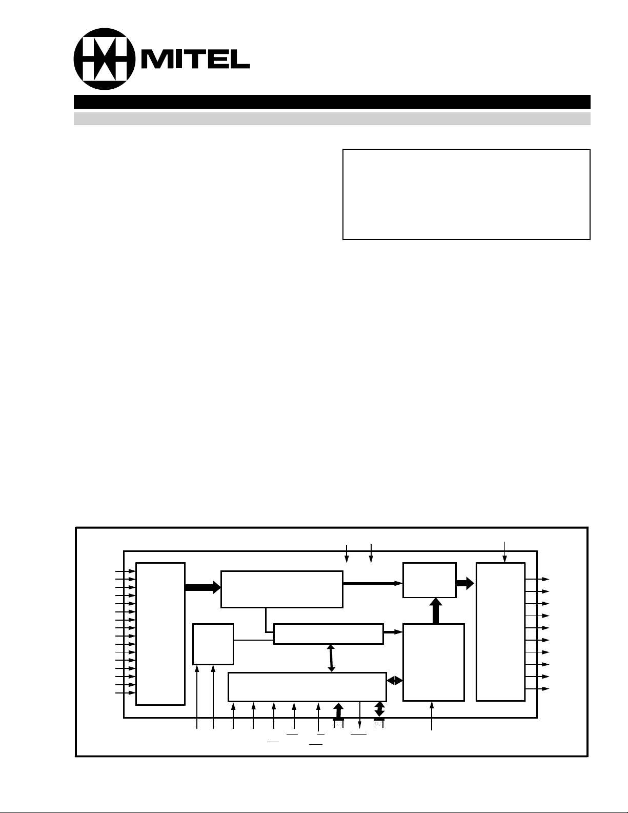
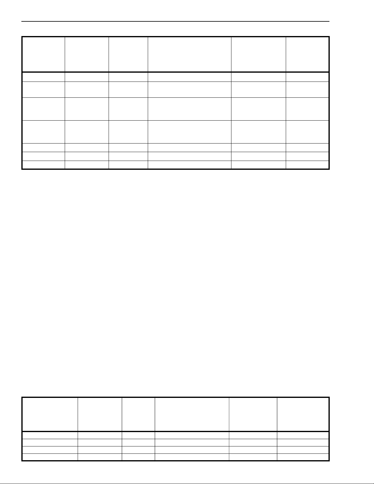
STi0
STi1
STi2
STi3
STi4
STi5
STi6
STi7
STi8
STi9
* STi10
* STi11
* STi12
* STi13
* STi14
* STi15
* 44 Pin only
Serial
to
Parallel
Converter
Timing
Unit
CLK FR AS/
ALEIM*
V
DDVSS
Multiple Buffer Data
Memory
Internal Registers
Microprocessor
Interface
DS
CS R/W
RD
WR
A0/
A7
DTA
AD7/
AD0
Connection
Figure 1 - Functional Block Diagram
Output
MUX
Memory
CSTo
ODE
Parallel
to
Serial
Converter
STo0
STo1
STo2
STo3
STo4
STo5
STo6
STo7
STo8 *
STo9 *
2-63
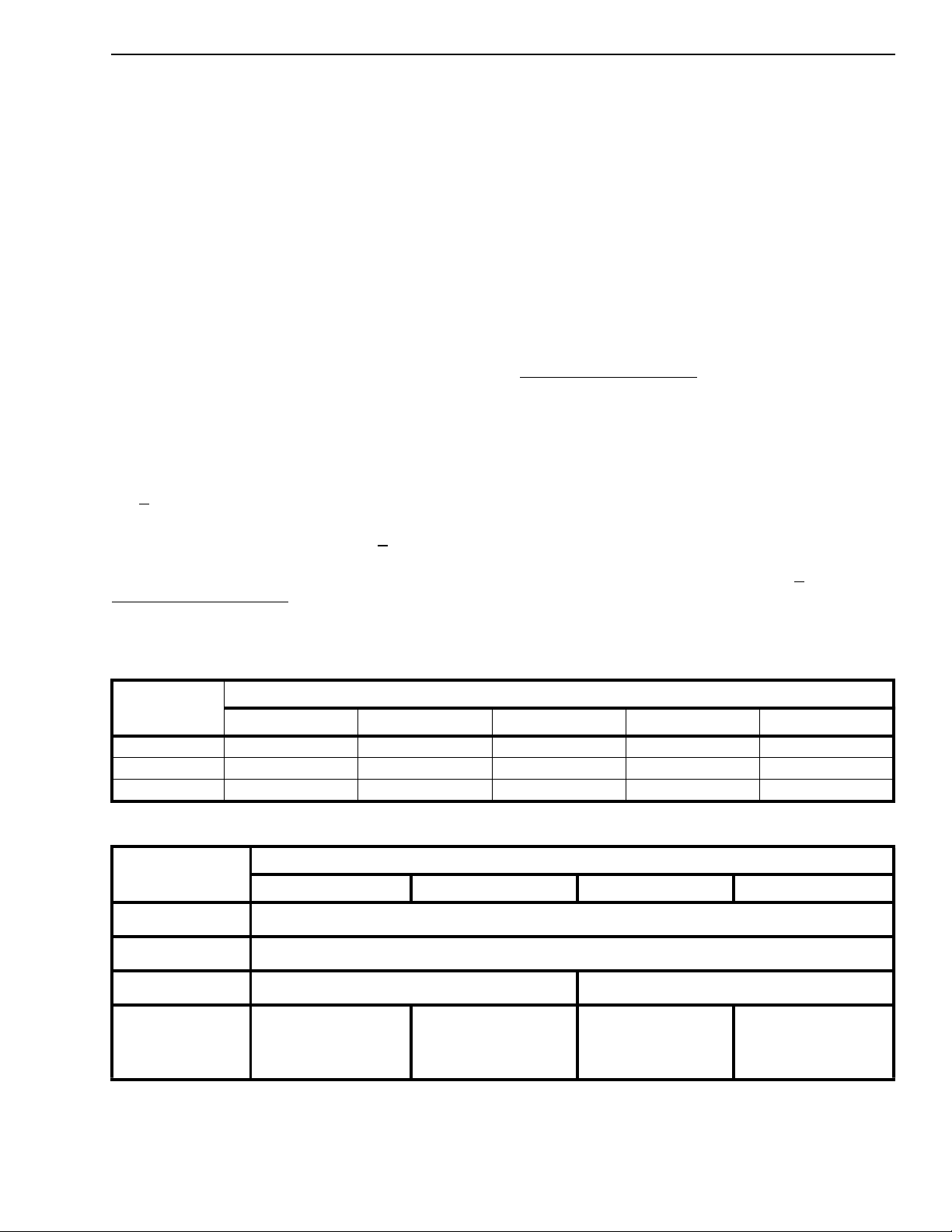
Page 2
MT8986
AS/ALE
ODE
STo0
STo1
STo2
CSTo
STi4/STo8
DTA
STi0
STi1
STi2
AS/ALE
ODE
STo0
STo1
STo2
CSTo
STi4/STo8
DTA
STi0
STi1
STi2
STi3
STi4
STi5
STi6/A6
STi7/A7
VDD
FR
CLK
STi8/A0
STi9/A1
STi10/A2
7
8
9
10
11
12
13
14
15
16
17
IM
STi11/A3
165432 44434241
231819 20 21 22 24 25 26 2728
DS/RD
STi3/A5
STi12/A4
R/W/WR
44 PIN PLCC
CS
40
STo3
39
38
STo4
37
STo5
36
STo6/A6
35
STo7/A7
34
VSS
33
AD0
32
AD1
31
AD2
30
AD3
29
AD4
AD5
AD6
AD7
STi15/STo9
FR
A0
A1
A2
A3
A4
A5
1
2
3
4
5
6
7
8
9
10
11
12
13
14
15
16
17
18
19
20
DTA
STi0
STi1
STi2
STi3
STi4
STi5
STi6/A6
STi7/A7
VDD
CLK
DS/RD
R/W\WR
STi6/A6
STi7/A7
STi8/A0
STi9/A1
STi10/A2
40
39
38
37
36
35
34
33
32
31
30
29
28
27
26
25
24
23
22
21
STi3
STi4
STi5
VDD
FR
CLK
CSTo
ODE
STo0
STo1
STo2
STo3
STo4
STo5
STo6/A6
STo7/A7
VSS
AD0
AD1
AD2
AD3
AD4
AD5
AD6
AD7
CS
4443424140
1
2
3
4
5
6
7
8
9
10
11
1213141516
IM
STi11/A3
STi12/A4
STi3/A5
44 PIN QFP
3837363534
39
17
1819202122
CS
DS/RD
R/W/WR
AD7
AD6
33
32
31
30
29
28
27
26
25
24
23
AD5
STo3
STo4
STo5
STo6/A6
STo7/A7
VSS
AD0
AD1
AD2
AD3
AD4
STi15/STo9
40 PIN DIP
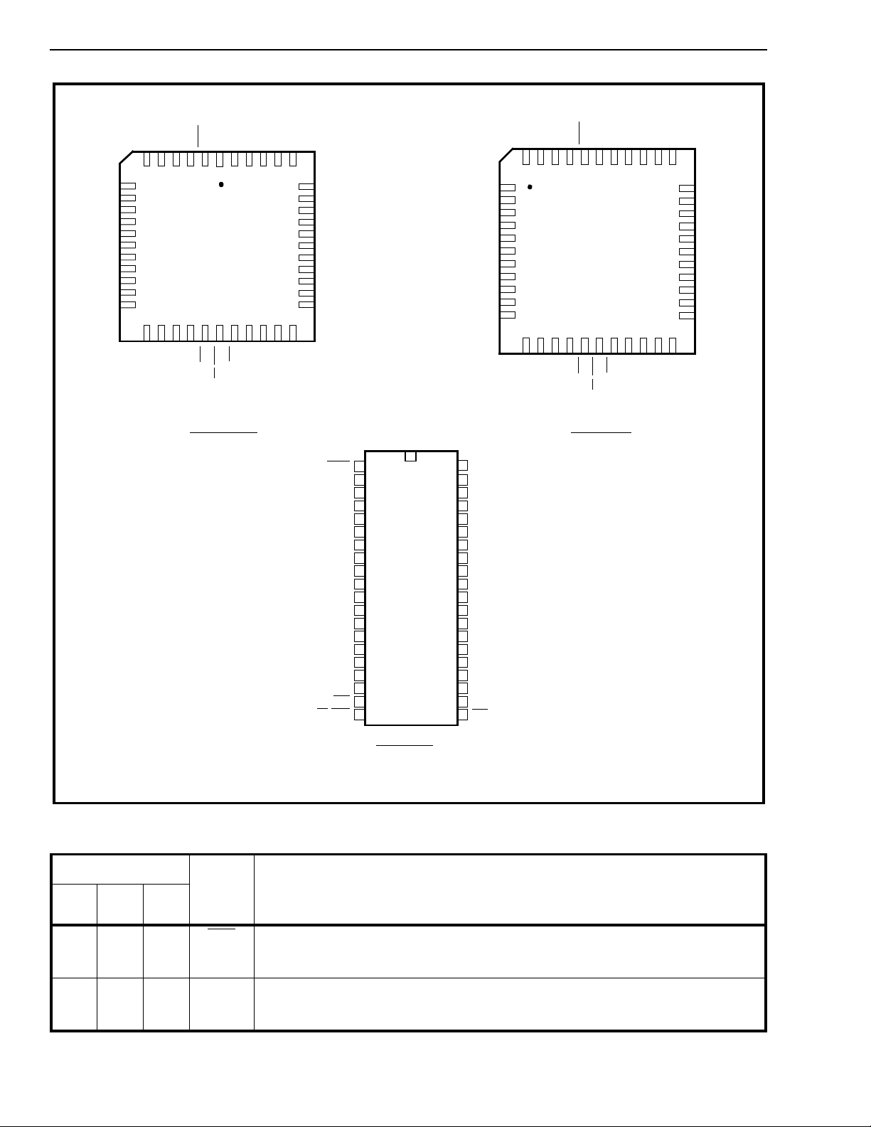
Figure 2 - Pin Connections
Pin Description
Pin #
40
DIP44PLCC44QFP
1240DTAData Acknowledgeme nt (Open Drain Out put ). This act ive l ow output indicates
2-7 2-5
2-64
7-9
41-43
1-3
Name Descri ption
that a data bus transfer is complete . A 10kΩ pull-up resistor is required at this
output.
STi0-5 ST-BUS Inputs 0 to 5 (Inputs). Serial data input streams. These streams may
have data rates of 2.048, 4.096 or 8.192 Mbi t/s with 32, 64 or 128 channels,
respectively.
Page 3
MT8986
Pin Description (continued)
Pin #
40
DIP44PLCC44QFP
8 10 4 STi6/ A6 ST-BUS Input 6/Ad dr.6 input (Input). The function of this pin is determined by
9 11 5 STi7/ A7 ST-BUS Input 7/Ad dr.7 input (Input): The function of this pin is determined by
Name Descri ption
the switching configura tion enabled . If non-multiplexed CP U bus is used along
with a higher input rate of 8.192 or 4.096 Mb/s, this pin provides A6 address
input function. For 2.048 and 4.096 Mb/s (8x4) applicati ons or when multiplexed
CPU bus (44 pin only) is selected, this pin assum es STi6 function. S ee Cont rol
Register bits description and Tables 1, 2, 6 & 7 for more details.
Note that for applicati ons where both A6 and STi6 inputs are required
simultaneously (e. g., 8 x 4 swi tching conf igura tion at 4.09 6 Mb/ s or rate
conversion between 2.048Mb/ s to 4.196 or 8.192 Mb/ s) the A6 input shoul d be
connected to pin STo6/A6.
the switching configura tion enabled . If non-multiplexed CP U bus is used along
with a higher input rate of 8.192 Mb/s, this pin provides A7 address input
function.
For 2.048 and 4.096 Mb/s (8x4 ) applications or when multiple xe d CPU bus
(44 pin only) is selected, this pin assumes STi7 function. See Control Register
bits descriptio n and Tables 1, 2, 6 & 7 for more details.
Note that for applicati ons where both A7 and STi7 inputs are required
simultaneously (e.g., 2.048 to 8.192 Mb/s rate co nversion) the A 7 input should
be connected to pin STo7/A7.
10 12 6 V
11 13 7 FR F ram e Pulse (Input). This input accepts and aut omatical ly ident ifies frame
12 14 8 CLK Clock (Input). Serial clock for shiftin g data in/out on the serial streams.
13-15 15-17 9-11 A0-2/
STi8-1 0
16-18 19-21 13-15 A3-5/
STi11-13
19 22 16 DS/RD
20 23 17 R/ W
+5 Volt Power Supply.
DD
synchronization signals formatted ac cording to ST-BUS and GCI interface
specifications.
Depending on the serial interface speed selected by IMS (Interface Mode Select)
register, the clock at this pin can be 4.096 or 8.192 MHz.
Address 0-2 / Input Stre ams 8-1 0 (Input). When non-multiplexe d CPU bus is
selected, these lines provide the A0-A2 address lines to MT8986 inte rnal
registers. When 16x8 switching conf iguration is se lecte d (in 44 pin only), then
these pins are ST-BUS serial inputs 8 to 10 receiving data at 2.048 Mb/s.
Address 3-5 / Input Stre ams 11-13 (Input). When non-multi plexed CP U bus is
selected, these lines provide the A3-A5 address lines to MT8986 internal
registers. When 16x8 switching conf iguration is se lecte d (in 44 pin only), then
these pins are ST-BUS serial inputs 11 to 13 receiving data at 2.048 Mb/s.
Data Strobe/Read (Input). When non-m ult iplexed CPU bus or Motoro la
multiplexed bus (44 pin only) are selected, this input is DS. This active high input
works in conjunction with CS
For Intel/Natio nal mu lti plexed bus (44 pin only), th is input is RD
input configures the data bus lines (AD0-AD7) as outputs.
\WR Read/Write \ Write (Input). In case of non-multiplexed and Motorol a multipl exed
buses (44 pin only), this input is R/W
bus lines (AD0-AD7) during a microprocessor access.
With Intel/Nat ion al multip lexed ti min g (44 pin only), thi s input is WR
low signal configures the data bus lines (AD0-AD7) as inputs.
to enable read and write operation.
. This active low
. This input controls the direction of the data
. This active
21 24 18 CS
22-29 25-27
29-33
30 34 28 V
19-21
23-27
AD7-
AD0
SS
Chip Se le c t (Input ). Active low input enabling a microprocessor read or write of
the control register or internal memories.
Data Bus (Bidirectional): These pins provide mic roprocessor access to the
internal control registers, connection memories high and low and data memories.
In multiplexed bus mode (44 pin) these pins also provide the input address t o the
internal Address Latch circuit.
Ground.
2-65
Page 4
MT8986
Pin Description (continued)
Pin #
40
DIP44PLCC44QFP
31 35 29 STo7/A7 ST-BUS Output 7/Address 7 inpu t (Three-state output/input). The function of
32 36 30 STo6/A6 ST-BUS Output 6/Address 6 inpu t (Three - state output/input). The function of
33-38 37-39
41-43
31-33
35-37
Name Descri ption
this pin is determined by the switching configurat ion enab led. If non-multipl exed
CPU bus is used along with data rates employing 8. 192 Mb /s rates, this pin
provides A7 address input function. For 2.048 Mb/s applications or when
multiplexe d CPU bus (44 pin only) is selected, t his pin as sumes S To7 function.
See Tables 1, 2, 6 & 7 for more details.
Note that for applicati ons where A7 input and STo7 outpu t are required
simultaneously (e.g., 8.19 2 to 2.048 Mb/s rate conver sion), the A7 input should
be connected to pin STi7/A7.
this pin is determined by the switching configurat ion enab led. If non-multipl exed
CPU bus is used along with a higher data rate employing 8.192 or 4.096 Mb/s,
this pin provides the A6 address input function. F or 2.048 Mb/s appli ca tio ns or
when multiplexed CPU bus (44 pin only) is selected, this pin assumes S To6
function. See Tables 1, 2, 6 & 7 for more details.
Note that for applicati ons where both A6 input and STo6 output are required
simultaneously (e.g., 4.096 to 2.048 Mb/s or 8.192 to 2.048 Mb/s rate conversion
applications), the A6 input should be connected to pin STi6/A6.
STo5-0 ST-BUS Outputs 5 to 0 (Three-state Output s). Serial data output stream s.
These serial streams may be composed of 32, 64 and 128 channels at data rates
of 2.048, 4.096 or 8.192 Mbit/s, respectively.
39 44 38 ODE Output Drive Enable (Input). This is the output enable input for the STo0 to
40 1 39 CSTo Control ST-BUS Output (Output). This is a 2.048 Mb/s o utput containing 256
- 6 AS/ALE Address Strobe or Latc h Enabl e (Inpu t). This input is only used if multiplexed
- 18 IM CPU Interface Mode (Input). If HIGH, this input configures MT 8986 in
- 28 STi15/
STo9
- 40 STi14/
STo8
STo9 serial outputs. If this input is low STo0-9 are high impedance. I f this input is
high each channel may still be put into high impedance by using per-channel
control bits in Connect Memory High.
bits per frame. The level of each bit is determined by the CSTo bit in the Connect
Memory high locations.
bus is selected via the IM input pin (44 pin only).
The falling edge of this signal is used to sample the add ress into the address
latch circuit. In case of non-multiplexed bus, this input is not required and should
be left open.
multiplexed microprocessor bus mode. If this input pin is not connected or
grounded, the MT8986 assumes non-mul tiplexed CP U interf ac e.
ST-BUS Input 15 / ST-BUS Output 9 (Input/three-stat e out put ). This pin is only
used if multiplexed CPU bus is selected. If 16-input x 8-output switching
configuration is enabl ed in the SCB bits (IMS register), th is pin is an input
receiving serial ST-BUS stream 15 at a data rate of 2.048 Mb it/s.
If Stream Pair Select ion capab ilit y is enabled (see switching conf igurat ion
section), this pin is the ST-BUS stream 9 output.
When non-multiplexed bus structu re is used, this pin should be left open.
ST-BUS Input 14 / ST-BUS Output 8 (Input/three-stat e out put ). This pin is only
used if multiplexed CPU bus is selected. If 16-input x 8-output switching
configuration is enabl ed in the SCB bits (IMS register), th is pin is an input that
receives serial ST-BUS stream 14 at a data rate of 2.048 Mbit/s.
If Stream Pair Select ion capab ilit y is enabled (see switching conf igurat ion
section), this pin is the ST-BUS stream 8 output.
When non-multiplexed bus structu re is used, this pin should be left open.
2-66
Page 5

MT8986
DEVICE OVERVIEW
With the integration of voice, video and data services
in the same network, there has been an increasing
demand for systems which ensure that data at N x
64 kbit/s rates maintain sequence integrity while
being transported through time-slot interchange
circuits. This requirement demands time-slot
interchange devices which perform switching with
constant throughput delay for wideband data
applications while guaranteeing minimum delay for
voice channels.
The MT8986 device meets the above requirement
and allows existing systems based on the MT8980D
to be easily upgraded to maintain the data integrity
when wideband data is transported. The device is
designed to switch 32, 64 or N x 64 kbit/s data. The
MT8986 can provide frame integrity for data
applications and minimum throughput switching
delay for voice applications on a per channel basis.
The serial streams of the MT8986 device can
operate at 2.048, 4.096 or 8.192 Mbit/s and are
arranged in 125 µs wide frames which contain 32, 64
and 128 channels, respectively. In addition, a built-in
rate conversion circuit allows the user to
interconnect various backplane speeds like 2.048 or
4.096 or 8.192 Mb/s while maintaining the control of
throughput delay function on a per-channel basis.
MT8986 device receives TDM serial data at different
rates and from different number of serial streams.
Data and Con nect Memo ries
For all data rates, the received serial data is
converted to parallel format by the serial to parallel
converters and stored sequentially in a Data
Memory. Depending on the selected operation
programmed in the IMS (Interface Mode Select)
register, the Data Memory may have up to 512 bytes
in use. The sequential addressing of the Data
Memory is performed by an internal counter which is
reset by the input 8 kHz frame pulse (FR) marking
the frame boundaries of the incoming serial data
streams.
Data to be output on the serial streams may come
from two sources: Data Memory or Connect Memory.
Locations in the Connect Memory, which is split into
HIGH and LOW parts, are associated with particular
ST-BUS output streams. When a channel is due to
be transmitted on an ST-BUS output, the data for the
channel can either be switched from an ST-BUS
input as in connection mode or it can be from the
Connect Memory Low as in message mode. Data
destined for a particular channel on the serial output
stream is read from the Data Memory or Connect
Memory Low during the previous channel time-slot.
This allows enough time for memory access and
parallel to serial conversion.
By using Mitel Message mode capability, the
microprocessor can access input and output timeslots on a per channel basis to control external
circuits or other ST-BUS devices. The MT8986
automatically identifies the polarity of the frame
synchronization input signal and configures its serial
port to be compatible to both ST-BUS and GCI
formats.
In the 44 pin packages, two different microprocessor
bus interfaces can be selected through an input
mode pin (IM): Non-Multiplexed or Multiplexed.
These interfaces provide compatibility with Intel/
National m ultiplexed and Motorola Multiplexed/NonMultiplexed buses. In 44 pin, the MT8986 provides a
16 x 8 switching configuration to form a 512 x 256
channel blocking matrix. Also, a flexible Stream Pair
Selection operation allows the software selection of
which pair of input and output streams can be
connected to an internal 128 x 128 matrix. See
Switching Configurations section for details.
Functional Description
A functional Block Diagram of the MT8986 device is
shown in Figure 1. Depending on the application, the
Connection and Mess age Mo des
In connection mode, the addresses of the input
source data for all output channels are stored in the
Connect memories High (CMH) and Low (CML). The
CML and CMH are mapped so that each location
corresponds to an output channel on the output
streams. The number of source address bits in CMH
and CML to be utilized varies according to the
switching configuration selected in the IMS register.
For details on the use of the source address data
(CAB and SAB bits), see CMH and CML bit description (Figures 5 & 6). Once the source address bits
are programmed by the CPU, the contents of the
Data Memory at the selected address are transferred
to the parallel-to-serial converters. By having the
output channel specify the source channel through
the connect memory, the user can route the same
input channel to several output channels, allowing
broadcast fa c i lity w ith i n th e switch.
In message mode the CPU writes data to the
Connect Memory Low locations corresponding to the
output link and channel number. The contents of the
Connect Memory Low are transferred directly to the
parallel-to-serial converter one channel before it is to
2-67
Page 6

MT8986
be output. The Connect Memory Low data is
transmitted on to the output every frame until it is
changed by the CPU with a new data.
The features of each output channel in the MT8986
are controlled by the Connect Memory High bits.
These bits determine individual output channels to
be in message or connection mode, select
throughput delay types and enable/disable output
drivers. The Connect Memory High also provides
additional stream and channel address bits for some
configurations. In addition, the Connect Memory
High provides one bit to allow the user to control the
CSTo output in 2.048 Mb/s applications.
If an output channel is set to high-impedance, the
TDM serial stream output will be placed in high
impedance during that channel time. In addition to
the per-channel control, all channels on the TDM
outputs can be placed in high impedance by pulling
the ODE input pin LOW. This overrides the individual
per-channel programming by the Connect Memory
High bits.
The Connect Memory data is received via the
Microprocessor Interface through the data I/O lines.
The addressing of the MT8986 internal registers,
Data and Connect memories is performed through
address input pins and some bits of the device's
Control register. The higher order address bits come
from the Control register, which may be written or
read through the microprocessor interface. The
lower order address bits come directly from address
input pins. For deta ils on the device addr essing, see
Software Control and Control register bits
description (Figure 3 & Tables 5, 6 and 7).
Serial D ata Interface
The master clock (CLK) can be either at 4.096 or
8.192 MHz allowing serial data link operations at
2.048, 4.096 and 8.192 Mb/s. These data rates can
be independently selected on input and output
streams allowing the MT8986 device to be used in
various speed backplanes and in rate conversion
applications. The selected data rates apply to the
inputs or the output streams. Different bit rates
among input streams or among output streams are
not allowed. Due to the I/O data rate selection
flexibility, two major operations can be selected:
Identica l or D i fferen t I/O data rate s.
and the number of the device's input and output
streams can be selected through the SCB bits
(Switching Configuration Bits) in the IMS register.
See Switching Configurations section for details.
Depending on the appl ication, the interface clock can
be selected to be twice the data rate or equal to the
data rate. This selection is performed through bit
CLKM in the IMS register. For applications where
both serial inputs and outputs are at 2.048 Mb/s (STBUS or GCI format), the CLKM bit should be set
LOW enabling the interface clock to be twice the bit
rate. In applications where both inputs and outputs
are at 4.096 or 8.192 Mb/s, CLKM should be set
HIGH enabling the interface clock to be equal to the
bit rate. In applications where inputs and outputs are
at different rates, the CLKM bit has no effect.
In applications with serial links at 2.048 Mb/s (see
Figures 16 to 19), the input 8 kHz frame pulse can be
in either ST-BUS or GCI format. The MT8986 device
automatically detects the presence of an input frame
pulse and identifies what type of backplane is
present on the serial interface. Upon determining the
interface connected to the serial port, the internal
timing unit establishes the appropriate transmit and
sampling edges. In ST-BUS format, every second
falling edge of the 4.096 MHz clock marks a bit
boundary and the input data is clocked in by the
rising edge, three quarters of the way into the bit cell.
In GCI format, every second rising edge of the 4.096
MHz clock marks the bit boundary while data
sampling is performed during the falling edge, at
three quarters of the bit boundaries.
For identical I/O rates at 4.096 and 8.192 Mb/s (see
Figure 20), the clock and interface data rates are
equal. The bit transmit and sampling edges vary
according to the applied frame pulse polarity. For
example, if the FR pulse polarity is positive, the bit
transmit operation is done on every rising edge of
CLK and the bit sampling on every falling edge. If
the FR pulse polarity is negative, these edges are
inverted. For different I/O rates, the MT8986 side
operating at 2.048 Mb/s data rate will comply with
ST-BUS or GCI interfaces for transmit and s ampling
procedures. The MT8986 side operating at 4.096 or
8.192 Mb/s behaves according to the frame pulse
polarity applied. See Figures 22 to 25.
Switching Configurations
The DMO bit (Device Main Operation) in the IMS
register is used for selecting between Identical I/O
rates or D i fferen t I/O rates. O n s yste m p ow e r- u p, th e
CPU should set up the DMO, the IDR (Input Data
Rate) and ODR (Output Data Rate) bits located in
the IMS register. When Identical I/O data rates are
selected by the DMO bit, the switching configuration
2-68
Switching configurations are determined basically by
the interface rates selected at the serial inputs and
outputs. To specify the switching configuration
required, the IMS register has to be initialized on
system power-up. In case of Identical I/O rates
(DMO bit LOW) at both inputs and outputs, the
switching configuration is selected by the two SCB
Page 7

MT8986
bits as shown in table 8 (see IMS register). In case of
different I/O rates (DMO bit HIGH), the switching
configuration is always non-blocking with different
number of I/O streams which is defined by the IDR
and ODR bits (see IMS register).
Identical Input/Output Data Rates
When identical input/output data rate is selected by
the DMO bit, th e I/O rate is de term ined b y th e ID R01 bits, and the ODR0-1 bits are ignored. For each
data rate specified by the IDR bits, different
switching configurations can be selected in the
SCB1-0 bits.
Serial Links with Data Rates at 2.048 Mb/s
When 2.048 Mb/s data rate is selected at the IDR
bits, four different I/O configurations can be selected
by the SCB1-0 bits (see Table 8); 8 x 8, 16 x 8, 4 x 4
with stream pair selection and nibble switching.
If 8 x 8 switching configuration is selected, a 256 x
256 channel non-blocking switching matrix is
available. In this configuration, the MT8986 device is
configured with 8 input and 8 output data streams
with 32 64 Kbit/s channels each. The interface clock
for this operation is 4.096 MHz with both ST-BUS
and GCI compatibilities and the per-channel
selection between variable and constant throughput
delay functions is provided. This configuration is
available in both the 40 and 44 pin packages.
register (SPS). The device clock for this operation is
4.096 MHz compatible to ST-BUS and GCI
interfaces. In addition, the per-channel selection
between variable or constant throughput delay is
available. This configuration is only provided in the
44 pin packages.
In case of nibble switching, 4-bit wide 32 kb/s data
channels can be switched within the device. In this
case, every serial stream is run at 2.048 Mb/s and
transports 64 nibbles per frame. When Nibble
Switching is selected at SCB bits, the MT8986
automatically assumes a 8 input x 4 output stream
configuration, providing a blocking switch matrix of
512 x 256 nibbles. If a non-blocking switch matrix is
required for nibble switching, the switch capacity is
reduced to 256 x 256 channel with a 4 input x 4
output configuration; the non-blocking matrix can be
arranged by the user by selecting any four of the 8
input streams. In nibble switching the interface clock
is 4.096 MHz.
Serial Links with Data Rates at 4.096 Mb/s
Two I/O configurations can be enabled by the SCB
bits when input and output data rates are 4.096 Mb/s
on each serial stream: 8 x 4 and 4 x 4. When 8 x 4
switching configuration is selected, a 512 x 256
channel blocking switch is available with serial
streams carrying 64, 64 Kb/s channels each. For this
operation, a 4.096 MHz interface clock equal to the
bit rate should be provided to MT8986. Only variable
throughput delay mode is provided.
In 16 x 8 switching configuration, a 512 x 256
channel blocking switch matrix is available. This
configuration is only provided in the 44 pin package
and when the CPU interface is configured in
multiplexed bus mode. The device clock in this
application is 4.096 MHz, ST-BUS or GCI
compatible. This configuration only provides variable
throughput delay.
If the stream pair selection switching configuration is
selected, only four input and four outputs (4 pairs of
serial streams) can be selected by the CPU to be
internally connected to the switch matrix, totalling a
128 x 128 channel non-blocking switch. From the 10
serial link pairs available, two pairs are permanently
connected to the internal matrix (STi0/STo0 and
STi1/STo1). An internal stream pair selection
capability allows two additional pairs of serial links to
be selected from the remaining 8 pairs (from STi/
STo2 to STi9/STo9) and be connected to the internal
matrix along with the permanently connected STi0/
STo0 and STi1/STo1 streams. The two additional pair
of streams called stream pair A and stream pair B,
should be selected in the Stream Pair Selection
In case of 4 x 4 switching configuration, a 256 x 256
channel non-blocking switch is available with serial
streams carrying 64, 64 Kb/s channels each. In this
configuration, the interface clock is 4.096 MHz and
the per-channel selection between variable and
constant throughput delay operation is provided.
Figure 20 shows the timing for 4.096 Mb/s operation.
Serial Links with Data Rates at 8.192 Mb/s
Only 2 input x 2 output stream configuration is
available for 8.192 Mb/s, allowing a 256 x 256
channel non-blocking switch matrix to be
implemented. To enable this operation, the IDR bits
should be programmed to select 8.192 Mb/s rates
and the SCB bits have no effect. At 8.192 Mb/s,
every input and output stream provides 128 timeslots per frame. The interface clock for this operation
should be 8.192 MHz. Figure 20 shows the timing for
8.192 Mb/s operation.
Table 1 summarizes the MT8986 switching
configurations for identical I/O data rates.
2-69
Page 8
MT8986
Interface
Serial
Interface
Data Rate
2 Mb/s 4.096 8x8 256x256 Non-Blocking STi0-7/STo 0-7 Yes
2 Mb/s
*
2 Mb/s
*
Nibble
Switching
(2 Mb/s)
4 Mb/s 4.096 8x4 512x256 Bloc king STi0-7/STo0-3 No
4 Mb/s 4.096 4x4 256x256 Non-Blocking STi0-3/STo0-3 Yes
8 Mb/s 8.192 2x2 256x256 Non-Blocking STi0-1/STo0-1 Yes
Table 1. Switching Configurations for Identical Input and Output Data Rates
* - only in the 44 pin packages
Different Inpu t/Outpu t Data Rat es
When Differen t I/O rate is selec ted by the DMO bit,
the input and output data rates should be selected at
the IDR and ODR bits, respectively. The Switching
Configuration Bits (SCB) are ignored with this
operation. This selection allows the user to multiplex
conventional 2.048 Mb/s serial streams into two
higher rates and vice-versa. In addition to the rate
conversion itself, the MT8986 allows for a complete
256 x 256 channel non-blocking switch at different
rates. In this operation, the per-channel variable/
constant throughput delay selection is provided.
Clock
required at
CLK Pin
(MHz)
4.096 16x8
4.096 10x10
4.096 8x4 512x256 Nibbles STi0-7/STo0-3 No
Number of
Input x
Output
Streams
*
*
Matrix
Channel
Capacity
512x256 Blocking STi0-15/STo0-7 No
128x128 Non-Bloc king
(on ly 4 inpu t x 4-output
can be selected)
Input Frame Offset Selection
When 4.096 or 8.192 Mb/s serial interfaces are
selected, the MT8986 device provides a feature
called Input Frame Offset allowing the user to
compensate for the varying delays at the incoming
serial inputs while building large switch matrices.
Usually, different delays occur on the digital
backplanes causing the data and frame
synchronization signals to be skewed at the input of
the switch device. This may result in the system
frame synchronization pulse to be active at the
MT8986 FR input before the first bit of the frame is
received at the serial inputs.
Input/Outpu t
Streams Used
STi0-9/STo0-9 Yes
Variable/
Constant
throughp ut
Delay
Selection
Depending on which data rates are programmed for
input and output streams, the number of data
streams used on the input and output as well as the
serial interface clock (CLK input pin) is different.
Once the CPU defines the data rates at the IDR and
ODR bits, the MT8986 automatically configures itself
with the appropriate number of input and output
streams for the desired operation. Table 2
summarizes the four options available when MT8986
is used with different I/O rates. Figures 22 to 25
show the timing for each of the four modes shown in
Table 2.
Interface
Input and
Output
Data Rates
2 Mb/s to 4 Mb/s 4.096 8x4 256x256 Non-Blocking STi0-7/STo0-3 Yes
2 Mb/s to 8 Mb/s 8.192 8x2 256x256 Non-Blocking STi0-7/STo0-1 Yes
4 Mb/s to 2 Mb/s 4.096 4x8 256x256 Non-Blocking STi0-3/STo0-7 Yes
8 Mb/s to 2 Mb/s 8.192 2x8 256x256 Non-Blocking STi0-1/STo0-7 Yes
2-70
Clock
require d at
CLK Pin
(MHz)
Table 2. Switching Configurations for Different I/O Data Rates
Number
of Input
x Output
Streams
When the input frame offset is enabled, an "internal
delay" of up to four clock periods is added to the
actual data input sampling, providing the MT8986
serial timing unit a new input frame reference. An
internal virtual frame is created which is aligned with
the framing of the actual serial data coming in at the
serial inputs and not with the FR frame pulse input.
In this operation, the transmission of the output
frame on the serial links is still aligned to the frame
pulse input signal (FR).
The selection of the data input sampling delay is
defined by the CPU in the Frame Input Offset
Variable/
Matrix
Channel Cap aci ty
Input/Outpu t
Streams Used
Constant
throughput
Selection
Delay
Page 9
MT8986
Register (FI O). If this functi on is not require d in the
user's applications, the FIO register should be set up
during system initialization to a state where offset
functions are disabled.
Delay Through the MT8 986
The switching of information from the input serial
streams to the output serial streams results in a
delay. Depending on the type of information to be
switched, the MT8986 device can be programmed to
perform time-slot interchange functions with different
throughput delay capabilities on a per-channel basis.
For voice applications, variable throughput delay can
be selected ensuring minimum delay between input
and output data. In wideband data applications,
constant throughput delay can be selected
maintaining the frame integrity of the information
through the switch.
The delay through the MT8986 device varies
according to the type of throughput delay selected in
the V
/C bit of the connect memory high.
Variable Throughput Delay Mode (V
/C b it = 0)
it is independent of the input and output streams.
The minimum delay achievable in the MT8986
depends on the data rate selected for the serial
streams. For instance, for 2.048 Mb/s the minimum
delay achieved corresponds to three time-slots. For
4.096 M b/s i t co rrespond s to five ti me-slots wh ile fo r
8.192 Mb/s it is nine time-slots. Switching
configurations with input and output channels that
provides more than its corresponding minimum
throughput delay, will have a throughput delay equal
to the difference between the output and input
channels; i.e., the throughput delay will be less than
one frame period. Table 3a shows the MT8986
throughpu t d e l ay fo r each data rate operat i on.
Different I/O Data Rates
Except for 2 Mb/s to 4 Mb/s and 2 Mb/s to 8 Mb/s
rate conversion operations, the throughput delay in
the MT8986 may vary according to the output stream
used for switching.
Table 3b explains the worst case conditions for the
throughput delay when different I/O data rate
switching configurations are used.
Identical I/O Data Rates
The delay in this mode is dependent on the
combination of source and destination channels and
Constant Throughput Delay mode (V
In this mode frame sequence integrity is maintained
in both Identical and Different I/O Data Rate
/C bit = 1)
Output Channel (# m)
Input Rate
m < n m=n, n+1, n+2 m= n+3, n+4 m=n+5, .. n+8 m > n+8
2.048 Mb/s 32-(n-m) t.s. m-n + 32 t.s. m-n t.s. m-n t.s. m -n t.s.
4.096 Mb/s 64-(n-m) t.s. m-n + 64 t.s. m -n+64 t.s. m-n t.s. m-n t.s.
8.192 Mb/s 128-(n-m) t.s. m-n + 128 t.s. m-n+128 t.s. m-n+128 t.s. m-n t.s.
Table 3a. Variable Throughput Delay Values for Identical I/O Rate Applications
n= inpu t channel, t.s . = time-s lo t
I/O Data Rate
Configu rati on
2 Mb/s to 4 Mb/s
2 Mb/s to 8 Mb/s
4 Mb/s to 2 Mb/s
8 Mb/s to 2 Mb/s
0, 1 2, 3 4, 5 6, 7
dmin=5x 4Mb/s t.s.
dmax=1 fr.+(4x 4Mb/s t.s.)
dmin=9x 8Mb/s t.s.
dmax=1 fr.+(8x 8Mb/s t.s.)
dmin=3x 2Mb/s t.s.
dmax=1 fr.+(2x 2Mb/s t.s.)
dmin=3x 2Mb/s t.s.
dmax=1 fr.+(2x 2Mb/s
t.s.)
dmin=(2x 2Mb/s t.s.)+
(3x 8Mb/s t.s.)
dmax=1 fr.+(1x 2Mb/s
t.s.)+(3x 8Mb/s t.s.)
Output Str eam U sed
dmin=(2x 2Mb/s t.s.)+(1x 4Mb/s t.s.)
dmax=1 fr.+(1x 2Mb/s t.s.)+(1x 4Mb/s t.s.)
dmin=(2x 2Mb/s t.s.)+
(2x 8Mb/s t.s.)
dmax=1 fr.+(1x 2Mb/s
t.s.)+(2x 8Mb/s t.s.)
dmin=(2x 2Mb/s t.s.)+
(1x 8Mb/s t.s.)
dmax=1 fr.+(1x 2Mb/ s
t.s.)+(1x 8Mb/s t.s.)
Table 3b. Min/Max Throughput Delay Values for Different I/O Rate Applications
Notes: dmin and dmax are measured in time-slots and at the point in time when the output channel is completely shifted out.
t.s. = tim e- sl ot
fr. = 125 µs frame
2 Mb/s t.s . = 3 .9 µs
4 Mb/s t. s. = 1.9 5 µs
8 Mb/ s t. s . = 0. 97 5 µs
2-71
Page 10
MT8986
Data Rate Throughput Delay (d)
2.048 Mb/s d=[32 + (32 - IN) + (OUT - 1)]; (expressed in # time-slot s)
2.048 Mb/s time-sl ot: 3.9µs
IN: input time-slot (from 1 to 32)
OUT: output time-slot (from 1 to 32)
4.096 Mb/s d=[64 + (64 - IN) + (OUT - 1)]; (expressed in # time-slot s)
4.096 Mb/s time-sl ot: 1.95 µs
IN: input time-slot (from 1 to 64)
OUT: output time-slot (from 1 to 64)
8.192 Mb/s d=[128 + (128 - IN) + (OUT - 1)]; (expressed in # time-slots)
8.192 Mb/s time-sl ot: 0.975 µs
IN: input time-slot (from 1 to 128)
OUT: output time-slot (from 1 to 128)
Table 4. Constant Throughput Delay values
operations by making use of a multiple Data-Memory
buffer techn ique. The input channels written in any of
the buffers during frame N will be read out during
frame N+2. In applications at 2.048 Mb/s for
instance, the minimum throughput delay achievable
in constant delay mode will be 32 time-slots; for
example, when input time-slot 32 (channel 31) is
switched to output time-slot 1 (channel 0). Likewise,
the maxim um delay is a chieved when the first tim e
slot in a frame (channel 0) is switched to the last
time-slot in the frame (channel 31), resulting in 94
time-slots of delay.
To summarize, any input time-slot from input frame N
will always be switched to the destination time-slot
on output frame N+2. Table 4 describes the MT8986
constant throughput delay values for different data
rates.
Microprocessor Port
The non-multiplexed bus interface provided by the
MT8986 device is identical to that provided in
MT8980 Digital Switch device. In addition to the nonmultiplexed bus, the MT8986 device provides an
enhanced microprocessor interface with multiplexed
bus structure compatible to both Motorola and Intel
buses. The multiplexed bus structure is available
only in the 44 pin packages and it is selected by the
CPU Interface Mode (IM) input pin.
If IM input pin is not connected (left open) or
grounded, the MT8986 parallel port assumes its
default Motorola non-multiplexed bus mode identical
to that of MT8980. If IM input is connected HIGH, the
internal parallel microport provides compatibility to
MOTEL interface allowing direct connection to Intel,
National and Motorola CPUs.
The MOTEL circuit (MOtorola and InTEL compatible
bus) automatically identifies the type of CPU Bus
connected to the MT8986 device. This circuit uses
the level of the DS/RD
input pin at the rising edge of
the AS/ALE to identify the appropriate bus timing
connected to the MT8986. If DS/RD
is LOW at the
rising edge of AS/ALE then Motorola bus timing is
selected . If DS/RD
is HIGH at the rising edge of AS/
ALE, then Intel bus timing is selected.
When MT8986 parallel port is operating in Motorola,
National or Intel multiplexed bus interfaces, the
signals available for controlling the device are: AD0AD7 (Data and Address), ALE/AS (Address Latch
Enable/Address Strobe), DS/RD
Read), R/W
Select) and DTA
\WR (Read/Write\Write), CS (Chip
(Data Acknowledgement). In
(Data Strobe/
Motorola non-multiplexed bus, the interface control
signals are: data bus (AD0-AD7), six address input
lines (A0-A5) and four control lines (CS
, DS, R/W
and DTA). See Figures 26 to 28 for each CPU
interface timin g.
The MT8986 parallel microport provides the access
to the IMS, Control registers, the Connection
Memory High, the Connection Memory Low and the
Data Memory. All locations can be read or written
except for the data memory which can be read only.
Softwar e Cont rol
The address bus on the microprocessor interface
selects the internal registers and memories of the
MT8986. If the A5 address input is LOW, then the
MT8986 Internal Control, Interface Mode, Stream
Pair Selection and Frame Input Offset registers are
addressed by the A4 to A0 bits according to Table 5.
If A5 input is HIGH, then the remaining address input
lines are used to select memory subsections of up to
128 locations corresponding to the maximum
number of channels per input or output stream. The
address input lines and the Stream Address bits
(STA) of the Control register give the user the
capability of accessing all sections of the MT8986
Data and Connect memories.
2-72
Page 11
MT8986
The Control and Interface Mode Selection registers
together control all the major functions of the device.
The Interface Mode Select register should be set up
during system power-up to establish the desired
switching configuration as explained in the Serial
Interface and Switching Configurations sections.
The Control register is dynamically used by the CPU
to control switching operations in the MT8986. The
Control register selects the device's internal
memories and its subsections to specify the input
and output channels selected for switching
procedures.
The data in the Control register consists of Split
memory and Message mode bits, Memory select and
Stream Address bits. The memory select bits allow
the Connect Memory HIGH or LOW or the Data
Memory to be chosen, and the Stream Address bits
define an internal memory subsections
corresponding to input or output ST-BUS streams.
Bit 7 (Slip Memory) of the Control register allows split
memory operation whereby reads are from the Data
memory and writes are to the Connect Memory
LOW.
The Message Enable bit (bit 6) places every output
channel on every output stream in message mode;
i.e., the contents of the Connect Memory LOW
(CML) are output on the ST-BUS output streams
once every frame unless the ODE input pin is LOW.
If ME bit is HIGH, then the MT8986 behaves as if bits
2 (Message Channel) and 0 (Output Enable) of every
Connect M emory H IGH ( CMH) loca tions we re set to
HIGH, regardless of the actual value. If ME bit is
LOW, then bit 2 and 0 of each Connect Memory
HIGH loc ation funct ion norm ally. In this case, if bit 2
of the CMH is HIGH, the associated ST-BUS output
channel is in Message mode. If bit 2 of the CMH is
LOW, then the contents of the SAB and CAB bits of
the CMH and CML define the source information
(stream and channel) of the time-slot that is to be
switched to an output.
If the ODE input pin is LOW, then all serial outputs
are high-impedance. If ODE is HIGH, then bit 0
(Output Enable) of the CMH location enables (if
HIGH) or disables (if LOW) the output drivers for the
corresponding individual ST-BUS output stream and
channel.
The contents of bit 1 (CSTo) of each Connection
Memory High location is output on CSTo pin once
every frame. The CSTo pin is a 2048 Mbit/s output
which carr ies 2 56 bits . If CSTo bi t is set HIGH, th e
corresponding bit on CSTo output is transmitted
HIGH. If CSTo bit is LOW, the corresponding bit on
the CSTo output is transmitted LOW. The contents of
the 256 CSTo bits of the CMH are transmitted
sequentially on to the CSTo output pin and are
synchron ous to t he 2.04 8 Mb /s ST-BUS stre ams. To
allow for delay in any external control circuitry the
contents of the CSTo bit is output one channel before
the corresponding channel on the ST-BUS streams.
For example, the contents of CSTo bit in position 0
(ST0, CH0) of the CMH, is transmitted
synchronously with ST-BUS channel 31, bit 7. The
contents of CSTo bit in position 32 (ST1, CH0) of the
A7 A6 A5 A4 A3 A2 A1 A0 Location
XX000000 Control Register
XX000001 Interface Mode Select Regist er
XX000010 Stream Pair Select Register
XX000011 Frame Input Offset Register
00100000 Channel 0*
0
•
•
0
01100000 Channel 32**
0
•
•
0
1
•
•
1
*: c h annels 0 to 31 are used i n 2 .0 48 M b/s (8 x 8, 16 x 8 an d 1 0 x 10)
**: channels 0 to 63 are used i n 4 .0 96 M b/s (N ib bl e Switching , 4 x 4 , 8 x 4 or D iffer en t I/O rates)
***: ch annels 0 to 127 are used in 8.192 Mb /s (2 x 2 or Di fferent I/O rates)
0
•
•
0
1
•
•
1
0
•
•
1
1
1
1
1
1
1
1
1
1
1
1
1
0
•
•
1
0
•
•
1
0
•
•
1
0
•
•
1
0
•
•
1
0
•
•
1
0
•
•
1
0
•
•
1
0
•
•
1
Table 5 . Add ress Me mory Map
0
•
•
1
0
•
•
1
0
•
•
1
1
•
•
1
1
•
•
1
0
•
•
1
Channel 1*
•
•
Channel 31*
Channel 33**
•
•
Channel 63**
Channel 64***
•
•
Channel 127***
2-73
Page 12

MT8986
CMH is transmitted during ST-BUS channel 31 bit
6. For more detailed description of the CSTo
operation, see section 6 of Application Note MSAN-
123.
The Bit V
Connect Memory High location allows the perchannel selection between Variable and Constant
throughput delay modes.
Initialization of the MT8986
On initialization or power up, the contents of the
Connection Memory High can be in any state. This
is a potentially hazardous condition when multiple
MT8986 ST-BUS outputs are tied together to form
matrices, as these outputs may conflict. The ODE
pin should be held low on power up to keep all
outputs in the high impedance condition.
During the microprocessor initialization routine, the
microprocessor should program the desired active
paths through the matrices, and put all other
channels into the high impedance state. Care
should be taken that no two ST-BUS outputs drive
the bus simultaneously. When this process is
complete, the microprocessor controlling the
matrices can bring the ODE signal high to relinquish
high impedance state control to the CMH
/C (Variable/Constant Delay) of each
0s.
b
2-74
Page 13

MT8986
Control Re giste r - Rea d/Write
76543210
SM ME STA3 MS1 MS0 STA2 STA1 STA0
BIT NAME DESCRIPTION
7 S M Split Memory. When 1, all subsequent reads are from the Data Memory and writes are to
the Connection Memory Lo w, except when the Control Register is accessed again. When
0, the Memory Select bits specify the m em o ry for subsequent opera tio ns. In either case,
the Stream Address Bits select the subsection of the memo ry which is made available .
6 ME Message Enable. When 1, the contents of the Connection Memory Low are output on the
Serial Output stream s except when in High Imped ance as set by the ODE inp ut. When 0,
the Connection Memory bits for each channel determine what is output.
5 STA3 Stream Address Bit 3. This bit is used in the 44 pin packages when 16 x 8 switching
configuration is selected. It is used with STA2-0 to select one of the 16 input data streams
whenever the Data Memor y is to be read. The programming of this bit has no effect in
other switching configurations.
4-3 MS1-0 Memory Select Bits. The memory select bits operate as follows:
0-0 - Not to be used
0-1 - Data Memory (read only from the CPU)
1-0 - Connection Memory Low
1-1 - Connection Memory High
2-0 STA2-0 The number expressed in binary notati on on these bits refers to the inp ut or output ST-
BUS stream which corresponds to the subsection of memory made accessible for
subsequent operations.
The use of these bits depends on the switching configuration as well as the device’s main
operation defined by the DMO bit of the Interface Mode Selection register. Tables 6 and 7
show the utilization of these bits according to the device’s main operation.
Figure 3 - Control Register Description
2-75
Page 14

MT8986
Input Address pi ns used to
select indivi dual
Connectio n and Data
Memory positions within the
selected sub section
Identical
I/O
Rate
# of Input x
Output
Streams
STA bits us ed to
select subsections
of the Data
Memory
STA bits used to
select
subsections of the
Connection
Memory
2 Mb/s 8x8 STA2, STA1, STA0 STA2, STA1, STA0 A4, A3, A2, A1, A0
2 Mb/s * 4x4 * STA1, STA0 STA1, STA0 A4, A3, A2, A1, A0
2 Mb/s * 16x8 * STA3, STA2, STA1,
STA2, STA1, STA0 A4, A3, A2, A1, A0
STA0
4 Mb/s 4x4 STA1, STA0 STA1, STA0 A6, A4, A3, A2, A1, A0
4 Mb/s 8x4 STA2, STA1, STA0 STA1, STA0 A6, A4, A3, A2, A1, A0
8 Mb/s 2x2 STA0 STA0 A7, A6, A4, A3, A2, A1, A0
Nibble Switch
8x4 STA2, STA1, STA0 STA1, STA0 A6, A4, A3, A2, A1, A0 **
(2 Mb/s)
Table 6. Use o f STA Bits for Identical I/O Data Rate Ope ration
* - only in the 44 pin packages.
** - for D a ta M em o ry R ea d o p era tio ns A0 is not r e qu ired since tw o ni bb le s are provid ed p er read acce ss .
Different
I/O
Rate
2 Mb/s to
4 Mb/s
2 Mb/s to
8 Mb/s
4 Mb/s to
2 Mb/s
8 Mb/s to
2 Mb/s
Input x
Output
Streams
Config.
STA bits used
to select
Data
Memory
subsections
8x4 STA2, STA1,
STA bits used
to select
Connectio n
Memory
subsections
STA1, STA0 A4, A3, A2, A1, A0 A6,
STA0
8x2 STA2, STA1,
STA0 A4, A3, A 2, A1, A0 A7, A6 , A4, A 3, A 2, A1,
STA0
4x8 STA1, STA0 STA2, STA1,
STA0
2x8 STA0 STA2, STA1,
STA0
Input Address pins used
to access individual
Data Memory
positio ns withi n the
selected subsection
A6,
A4, A3, A2, A1, A0 A4, A3, A2, A1, A0
A7, A6, A4, A3, A2, A1, A0A4, A3, A2, A1, A 0
Input Address pins used
to access individ ual
Connection Memo ry
positions within the
selected subsection
A4, A3, A2, A1, A0
A0
Table 7. Us e of STA Bits for Different I/O Da ta Ra te Opera tion
Note: In rate conver s io n ap pl ic ati on s , D a ta Me m ory s ub s ec ti on s h a ve di ff ere nt s iz es th an C o nn ec ti on M em ory subsec ti on s. T his
implies th at different ad dr e s s inp u ts are u se d to select in di vi du al position s w ith in th e su bs e ct io ns fo r each type of m em ory.
2-76
Page 15

MT8986
Interface Mod e Selection Regist er - Read/Write
76543210
DMO IDR1 IDR0 ODR1 ODR0 SCB1 SCB0 CLKM
BIT NAME DESCRIPTION
7 DMO Device Main Operation . This bit is used by the CPU to define one of the two main
operations of the MT8986 device. If this bit is LOW, the MT8986 is configured for
identical I/O data rates. For this operation, the user should also specify the switching
configuration thro ugh the SCB bits.
If this bit is HIGH, the MT8986 device is configured in Different I/O data rate. This allows
combinations of input and output data rat es as shown in Table 2. The SCB bit s have no
effect in this application and the device is in Non-Blocking switch configuration with a 256
x 256 channel capacity.
6-5 IDR1-0 Input Data Rate Selection. These two bits select three different data rates for the inputs
of the MT8986. In the case of identical I/O rates (DMO bit = 0), these bits also determine
the serial output data rate.
IDR1 IDR0 Input Rate
0 0 2.048 Mb/ s
0 1 4.096 Mb/ s
1 0 8.192 Mb/ s
1 1 reserved
4-3 ODR1-0 Ou tput Data Rate Selection . These bits are only used when Different I/O rates are
selected (DMO bit=1 ). These tw o bits select t hree differen t data rates for the serial
outputs of the MT8986. These bits are ignored if DMO bit = 0.
ODR1
0 0 2.048 Mb/s
0 1 4.096 Mb/s
1 0 8.192 Mb/s
1 1 reserved
2-1 SCB1-0 Switchi ng Confi guratio n Bits 1-0. These bits should only be used when DMO is set
LOW. The use of these bits to select the switching configuration of the MT8986 device is
described in Table 8.
0 CLKM Clock Mode. This bit is only used when the MT8986 device is set to operate in identical
I/O data rates. When set High, thi s bit selects the interf ace clo c k to be equal to the bit
rate. If Low, this bit sele cts the interf a ce clock to be twice the bit rate.
For Different I/O data rate app lications, this bit is ignored.
Figure 4 - IMS Register Description
ODR0 Ou tput R ate
2-77
Page 16

MT8986
DMO Bit
Data Rate Selected
at IDR bits (M b/ s)
LOW
Identical
I/O
Rates
HIGH
Different I/O
Rates
** 44 pin packages only
Input/Outp ut Rate
SCB1 SCB0 Configuration
0 0 8 inputs x 8 output s - Non Blocking
0 1 16 inputs x 8 outputs - Blocking**
2.048
1 0 Stream pair selection capability (internal channel
capacity = 128 x 128) -
Non Blocking**
1 1 Nibble Switching - 8 inputs x 4 outputs - Blocking
0 0 8 inputs x 4 outputs - Blocking
0 1 4 inputs x 4 outputs - Non-Blocking
4.096
1 0 Reserved
1 1 Reserved
8.192
no
effectnoeffect
2 inputs x 2 outputs - Non-Blocking
no
selected in
effectnoeffect Reserved
IDR/ODR bits
Table 8. Switching Configurations for Identical I/O Rates
2-78
Page 17

Connection Mem ory High - Read/Writ e
76543210
XV/C SAB3 CAB6 CAB5 MC CSTo OE
(CM high bits)
BIT NAME DESCRIPTION
MT8986
6V
/C Variable/Constant Throughput Delay Mode. This bit is used to select between Variable
(LOW) and Constant Delay (HIGH) modes in a per-channel basis. Tables 1 and 2
describe the switching configuration s that have this function. In the modes where this
function is not availabl e, th is bit has not effect.
5 SAB3 Source Stre am Addr ess bit 3. This bit is used along with bits SAB0 -2 in CML to select
up to 16 different source streams for the connection. Depending on the state of DMO bit
and the switching configuration enabled, not all SAB 3-0 bits have to be used.
See Tables 9 and 10 for details on the utilization of the SAB bits.
4-3 CAB6-5 Source Chan nel Addr ess bits 5 and 6. These two bits are used together with bit s
CAB0-4 in Connect M emo ry Low to select up 128 different sou rce channels for the
connection. Dependin g on the data rate used in the inp ut/out put streams, 5, 6 or all 7
CAB bits can be used respectively, to select 32, 64 or 128 different channe l s.
See Tables 9 and 10 for detail s on the utilizati on of the CAB bits.
2 MC Message Channel. When 1, the conten ts of the corresponding locat ion in Connection
Memory Low are output on the corresponding channel and stream. When 0, the contents
of the programmed location in Connection Mem ory Low act as an address for the Data
Memory and so determine the sour ce of the connection to the location’s channel and
stream.
1 CSTo CSTo Bit. This bit is only available in 2.048 Mb/s applications. It drives a bit time on the
CSTo output pin.
0 OE Output Enable. This bit enables the output drivers on a per-channel basis. This allows
individual channels on individual streams to be made high-impedance, allowing switch
matrices to be constructed. A HIGH enables the driver and a LOW disables it.
Figure 5 - Connection Memory High (CMH) Bits
x=Do n’t c a r e
2-79
Page 18

MT8986
Connection M em ory L ow - Re ad/Write
76543210
SAB2 SAB1 SAB0 CAB4 CAB3 CAB2 CAB1 CAB0
(CM low bits)
BIT NAME DESCRIPTION
7-5 SAB2-0* Source Stre am Addr ess bits. These three bit s are used together wit h SAB 3 in CMH to
select up to 16 different source streams for the connection. Depending on the switching
configuration and the data rate selected in the application, 1, 2, 3 or all 4 SAB bits can be
used. See Tabl es 9 and 10 for detail s.
4-0 CAB4-0* Sou rce Chan nel Addr ess bi ts 0-4. These five bits are use d together wit h CAB 5-6 in
CMH to select up 128 different source channels fo r the connection. Depe nding on th e
switching confi gurat ion and the data rate used in the application, 5, 6 or all 7 CAB bits
can be used to select respectively 32, 64 or 128 different channels.
See Tables 9 and 10 for details.
If bit two (MC) of the corresponding Connection High locations is 1, or if bit 6 of the Control Register is 1, then these entire eight bits are output
on the corresponding output chann el and stream associated with this location . Otherwise, the bits are used as indicated to define the source
of the connection which is outp ut on the channe l and stream as sociat ed with this loca tion.
Figure 6 - Conne ction Mem ory Low (CML) Bi ts
Identical
I/O
Rate
# of Input x
Output
Streams
CAB bits used to determine the source
channel for the conne ctio n
SAB bits used to
determine the sou rce
stream for the
connection
2 Mb/s 8x8 CAB4 to CAB0 (32 channel/inp. stream) SAB2, SAB1, SAB0
2 Mb/s * 4x4 * CAB4 to CAB0 (32 channel/inp. stream) SAB2, SAB1
2 Mb/s * 16x8 * CAB 4 to CAB0 (32 channel/ inp. stream) SAB3, SAB2, SAB1, SAB0
4 Mb/s 4x4 CAB5 to CAB0 (64 channel/inp. stream ) SAB2, SAB1
4 Mb/s 8x4 CAB5 to CAB0 (64 channel/inp. stream) SAB2, SAB1, SAB0
8 Mb/s 2x2 CAB6 to CAB0 (128 channel/ inp. stream ) SAB2
Nibble Switch
8x4 CAB5 to CAB0 (64 nibble/inp. stream) SAB2, SAB1, SAB0
(2 Mb/s)
Table 9. CAB and SAB Bits Programming for Identical I/O Rate Applications
* - only in 44 pin package
Different
I/O
Rate
# of Input x
Output Streams
CAB bits used to determine the sour ce
channel for the connec tion
SAB bits used to
determine the sou rce
stream for the
connection
2 Mb/s to 4 Mb/s 8x4 CAB4 to CAB0 (32 channel/inp. stream) SAB2, SAB1, SAB0
2 Mb/s to 8 Mb/s 8x2 CAB4 to CAB0 (32 channel/inp. stream) SAB2, SAB1, SAB0
4 Mb/s to 2 Mb/s 4x8 CAB5 to CAB 0 (64 channel/inp. stream) SAB2, SAB1
8 Mb/s to 2 Mb/s 2x8 CAB6 to CAB0 (128 channel/inp. stream ) SAB2
Table 10. CAB and SAB Bits Programming for Different I/O Rate Applications
2-80
Page 19

MT8986
Stream Pair Selection Register - Read/Write (ONLY PROVIDED IN THE 44 PIN PACKAGES)
76543210
X X SPA2 SPA1 SPA0 SPB2 SPB1 SPB0
BIT NAME DESCRIPTION
5-3 SPA2-0 S tream Pair A sele ctio n. These three bits define which pair of streams a re going to be
connected to the switch matrix, together with the permanent ly connected strea ms
STi0-1 / STo0-1.
SPA2
0 0 0 STi 2 / STo2
0 0 1 STi 3 / STo3
0 1 0 STi 4 / STo4
0 1 1 STi 5 / STo5
1 0 0 STi 6 / STo6
1 0 1 STi 7 / STo7
1 1 0 STi 8 / STo8
1 1 1 STi 9 / STo9
2-0 S PB 2-0 Stream Pair B selection. These three bits define which pair of streams are going to be
connected to the switch matrix, together with the permanent ly connected strea ms
STi0-1 / STo0-1.
SPB2
0 0 0 STi2 / STo2
0 0 1 STi3 / STo3
0 1 0 STi4 / STo4
0 1 1 STi5 / STo5
1 0 0 STi6 / STo6
1 0 1 STi7 / STo7
1 1 0 STi8 / STo8
1 1 1 STi9 / STo9
These bits are only used when the Switching Configuration bits enable stream pair selection capability (SCB 1-0 =10) and the Input Data Rate
Selectio n bits enab le 2 Mb/s operati on (IDR-0 = 00). In all other modes, the cont en ts of this regist er are ignored .
Figure 7 - Stream Pair Selection (SPS) Register
x=Do n’t c a r e
Frame Input Offset Register - Read/Write
SPA1 SPA0 Stream Pair A Connected
SPB1 SPB0 Stream Pair B Connected
76543210
OFB2 OFB1 OFB0 X X X X X
BIT NAME DESCRIPTION
7-5 OFB2-0 Offset Bits 2-0. These three bits defi ne the time it takes the Serial Interface receiver to
recognize and store the first bit of the serial input streams; i.e., to start assuming a new
internal frame. The input frame offset can be selected to be up to 4 CK clock periods from
the time when frame pulse input signal is applied to the FR input .
OFB2
OFB1 OFB0 Number of Clock Periods
0 0 0 Normal Operat ion. No bit offsetting.
00 1 1
01 0 2
01 1 3
10 0 4
1 0 1 Reserved
1 1 0 Reserved
1 1 1 Reserved
If frame input offset operation is not requi red, this reg ister shou ld be cleared by the CPU during system initializa tio n.
Figure 8 - F rame In put O ffset (FIO ) Regist er
x=Do n’t c a r e
2-81
Page 20

MT8986
Applications
delay. This can be selected by the V
Connection Memory High locations.
Switch Matrix Architectures
Different connectivities at different data rates can be
The MT8986 is an ideal device for designs of
medium size switch matrix. For applications where
voice and grouped data channels are transported
within the same frame , th e voice sample s ha v e to b e
time interchanged with a minimum delay while
built to accommodate Non-Blocking matrices of up to
512 channels while maintaining the per channel
selection of the device's throughput delay. Some
examples of such Non-Blocking configurations are
given in Figures 9 to 11.
maintaining the integrity of grouped data. To
guarantee the integrity of grouped data during
switching and to provide a minimum delay for voice
connections, the MT8986 provides the per-channel
selection between variable and constant throughput
8 Streams
@ 2.048 Mb/s
IN OUT
8 Streams
@ 2.048 Mb/s
For applications where voice and data samples are
encoded into individual 64 kb/s time-slots on an
8kHz frame b a si s, th e s w itch ma trix can opera te with
time interchange procedures where only variable
8 Streams
MT8986
#1
MT8986
#2
@ 2.048 Mb/s
8 Streams
@ 2.048 Mb/s
/C bit of the
MT8986
#3
MT8986
#4
Figure 9 - 512-Channel Switch with Serial Streams at 2.048 Mb/s
STi0
STi1
STi2
STi3
MT8986
STo0
STo7
•
•
•
•
•
•
8 Streams
@ 2.048 Mb/s
IN
8 Streams
@ 2.048 Mb/s
STi0
•
•
•
•
•
•
STi7
MT8986
STo0
STo1
STo2
STo3
4 Streams
@ 4.096 Mb/s
Figure 10 - 256-Ch ann el Switc h with Rate Co nvers ion b etwee n 2.048 and 4.0 96 Mb/ s
IN
8 Streams
@ 2.048 Mb/s
STi0
•
•
•
•
•
•
STi7
MT8986
STo0
STo1
2 Streams
@ 8.192 Mb/s
STi0
STi1
MT8986
STo0
STo7
•
•
•
•
•
•
8 Streams
@ 2.048 Mb/s
OUT
OUT
2-82
Figure 11 - 256-Chan nel Swi tch w ith Ra te Con vers ion be tween 2.048 an d 8. 192 M b/s
Page 21

MT8986
throughput delay is guaranteed. For such
applications, the MT8986 device allows cost
effective implementations of Non-Blocking matrices
ranging up to 1024 channels. Figures 12 and 13
show the block diagram of implementations with
Non-Blocking capacities of 512 and 1024-channel,
respectively.
Interfacing MT8986 with 8051
The Intel 8051 is a very cost effective solution for
many applications that do not require a large CPU
interaction and processing overhead. However, in
applications where 8051 is connected to peripherals
operating on a synchronous 8 kHz time-base like the
MT8986, some connectivity issues have to be
addressed. The MT8986 may hold the CPU read/
write cycle due to internal contention between the
MT8986 microport and the internal serial to parallel
8 Streams
16 Streams
@2. 048 Mb/s
16
IN OUT
MT8986
512 x 256
MT8986
512 x 256
@2.048 Mb/s
8
8
8 Streams
@2.048 Mb/s
and parallel to serial converters. Since the 8051
family of CPUs do not provide Data Ready type of
inputs, some external logic and software
intervention have to be provided between the
MT8986 and the 8051 microcontrollers to allow read/
write operation. The external logic described in
Figure 14 is a block diagram of a logical connection
between MT8986 and 8051. Its main function is to
store the 8051 data during a write and the MT8986
data during a read.
For a write, MT8986 address is latched by the
internal address latch on the falling edge of the ALE
input. Whenever a read or write operation is done to
the MT8986 device, the address decoded signal
(MTA
) is used to latch or "freeze" the state of RD,
, and the ALE signals, until the data acknow-
WR
ledge output signal is provided by the MT8986
device, releasing the latches for a new read/write
cycle. Latch U5 is used to hold the 8051 data for a
write until the CPU is ready to accept it (when DTA
4 Streams
8 Streams
@4.096 Mb/s
8
IN OUT
MT8986
512 x 25 6
MT8986
512 x 25 6
@4. 096 Mb/s
4
4
4 Streams
@4. 096 Mb/s
Figure 12 - 51 2-C hanne l Non -Block ing S witc h Matri x with Serial S trea ms at 2.048 or 4.09 6 Mb /s
8
8
8
8
8 Streams
@2. 048 Mb/s
8 Streams
@2. 048 Mb/s
8 Streams
@2. 048 Mb/s
8 Streams
@2. 048 Mb/s
OUT
OUT
IN
IN
16 Streams
@2.048 Mb/s
16 Streams
@2.048 Mb/s
16
16
MT89 86
512 x 256
MT89 86
512 x 256
MT89 86
512 x 256
MT8986
512 x 256
MT8986
512 x 256
MT8986
512 x 256
MT8986
512 x 256
MT89 86
512 x 256
Figure 13 - 1024-Channel Non-Blocking Switch Matrix with Serial Streams at 2.048 Mb/s
2-83
Page 22

MT8986
RES
RST
8051
AD0
AD1
AD2
AD3
AD4
AD5
AD6
AD7
ALE
RD
WR
8
MT8986
8
Address
Decode
CS
DCKQ
PR
DCKQ
PR
DCKQ
MTA
MT8986
Access
LRD
LWR
LATCH LATCH
LE OE
OE LE
MT8986
AD0
AD1
AD2
AD3
AD4
AD5
AD6
AD7
ALE
WR
RD
CS
RD
MTA
DTA
MTA
AD0-AD7
DTA
PR
DTA
Figure 14 - Inte rfacin g the MT 89 86 to the 80 51 Mi cro cont roller
goes low). Latch U4 stores the MT8986 output data
during a read cycle wh enever DTA
goes low. When
writing to the MT8986, one write operation is
sufficient. However, when reading MT8986, two read
operations with the same address are required, with
the second being valid.
RES
R
C
Enough time need to be provided between two CPU
accesses to allow th e first access to complete; i.e.,
to allow for an internal MT8986 reaction over the first
RD
/WR access. For a read operation, a minimum of
1220 ns have to be guaranteed between two
successive accesses. For write, at least 800 ns has
to be respected.
2-84
Page 23

Absolute Maximum Ratings*
Parameter Symbol Min Max Units
MT8986
1V
2 Voltage on Digital Inputs V
3 Voltage on Digital Output s V
4 Current at Digital Outputs I
5 Storage Temperature T
6 Package Power Dissipation P
* Exceeding these values may cause perm an ent dama ge. Functi onal operati on under these cond ition s is not implie d.
Recommended Operating Conditions - Voltages are with respect to ground (V
1 Operating Temperature T
2 Positive Supply V
3 Input Voltage V
‡ Typ ical figures are at 25°C and are for desi gn aid only: not guarante ed and not subject to prod ucti on testin g.
DC Electrical Characteristics - Voltages are with respect to ground (V
1
2 Input High Voltage V
3 Input Low Voltage V
4 Input Leakage (input pins)
5 Input Pin Capacitance C
6
7 Outpu t High Current I
8 Outpu t Low Voltage V
9 Outpu t Low Current I
10 High Impedance Leakage I
11 Output Pin Capacitance C
‡ Typ ical figures are at 25°C and are for desi gn aid only: not guarante ed and not subject to prod ucti on testin g.
- V
DD
SS
Characteristics Sym Min Typ
Characteristics Sym Min Typ
Supply Current I
I
N
P
U
T
Input Leakage (I/O pins)
S
Output High Voltage V
O
U
T
P
U
T
S
‡
OP
DD
-40 25 +85 °C
4.75 5.0 5.25 V
I
DD
I
0V
‡
10 15 mA Outputs unloaded
2.0 V
IH
IL
IL
34
8pF
8pF
OH
OH
OL
OZ
I
2.4 V IOH = 10 mA
10 15 mA Sourcing. VOH=2.4V
OL
5 10 mA Sinking . VOL = 0.4V
O
-0.3 7 V
I
O
O
S
D
VSS-0.3 VDD+0.3 V
VSS-0.3 VDD+0.3 V
-65 +150 °C
) unless otherwise stated.
SS
Max Units Test Con ditio ns
DD
) unless otherwise stated.
SS
V
Max Units Test Conditio ns
0.8 V
5
µAV
between VSS and V
I
100
0.4 V IOL = 5 mA
5 µAVO between VSS and V
40 mA
2W
DD
DD
Output
Pin
Test Point
C
L
R
L
S1
V
SS
Figure 15 - Output Test Load
S2
V
SS
V
DD
S1 is open circuit except
when testing output levels
or high impedance states.
S2 is switched to V
when tes ting output
V
SS
levels or high impedance
states.
DD
or
2-85
Page 24

MT8986
_
AC Electrical Characteristics
Voltages are with respect to ground (VSS) unless otherwise stated.
Characteristics Sym Min Typ
†
ST-BUS Timing (2.048 Mb/s)
‡
Max Units Test Conditions
1 Fra me Pulse widt h t
2 Frame Pulse setup time t
3 Fra me Pulse hold t im e t
4 STo delay Active to Active t
5 STi setup time t
6 STi hold time t
7 Clock period t
8 CK Inpu t Low t
9 CK Inpu t High
10 Clock Rise/Fall Time
† Timing is over recommended temperature & power supply voltages (V
‡ Typ ical figures are at 25°C and are for desi gn aid only: not guarante ed and not subject to producti on testin g.
t
FRW
FR
t
FRH
FRW
FRS
FRH
DAA
STIS
STIH
CLK
CL
t
CH
t
r,tf
10 190 ns
20 190 ns
20 ns
20 ns
190 244 300 ns
85 122 150 ns
85 122 150 ns
244 ns
45 100 ns CL=150 pF
10 ns
=5V±5%, VSS=0V, TA=–40 to 85°C).
DD
t
CLK
t
CH
t
CL
2.0V
0.8V
STi
STo
STi
Ch. 31
Bit 0
Ch. 31
Bit 0
t
FRS
t
DAA
Ch. 0
Bit 7
t
STIS
Ch. 0
Bit 7
t
STIH
Figure 16 - ST-BUS Timing (CLKM bit=0)
t
r
Ch. 0
Bit 6
t
f
Ch. 0
Bit 6
Ch.0
Bit 5
Ch. 0
Bit 5
2.0V
0.8V
2.0V
0.8V
2.0V
0.8V
2-86
Page 25

AC Electrical Characteristics
Voltages are with respect to ground (VSS) unless otherwise stated.
†
- GCI Timing (2.048 Mb/s)
Characteristics Sym Min Typ
‡
Max Units Test Conditions
MT8986
1 Clock Period t
2 Pulse Width t
CL
3 Frame Width High t
4 Frame Setup t
5 Frame Hold t
6 Data Delay/Clock Active to
WFH
FRS
FRH
t
DAA
CK
, t
CH
150 244 300 ns
73 122 150 ns
244 ns
10 190 ns
20 190 ns
45 100 ns CL=150 pF
Active
7 Serial Input Setup t
8 Serial Input Hold t
9 Clock Rise/Fall Time t
† Timing is over recommended temperature & power supply voltages (V
‡ Typ ical figures are at 25°C and are for desi gn aid only: not guarante ed and not subject to prod ucti on testin g.
CLK
FR
STIS
STIH
r, tf
20 ns
20 ns
10 ns
=5V±5%, VSS=0V, TA=–40 to 85°C).
DD
STi/
STo
CLK
FR
STo
STi
Ch. 31
Bit 0
See Detail a
t
r
t
f
Detail a
t
DAA
t
FRS
Ch. 0
Bit 7
t
t
WFH
t
FRH
CL
Ch. 0
Bit 6
Note: bit 0 identifies the first bit of the GCI frame
t
CH
STIS
t
STIH
t
Ch. 0
Bit 5
t
CK
2.0V
0.8V
Ch. 0
Bit 4
2.0V
0.8V
2.0V
0.8V
2.0V
0.8V
Figure 17 - GCI Timing (CLKM bit=0)
2-87
Page 26

MT8986
AC Electrical Characteristics† - Serial Stream s fo r ST-BUS and GCI Backplanes (2.048 Mb/s)
Characteristics Sym Min Typ
‡
Max Uni ts Test Conditions
O
1
2 STo0/9 Delay - High Z to Active t
3 Output Driver Enable Delay t
4 CSTo Output Delay t
† Timing is over recommended temperature & power supply voltages.
‡ Typ ical figures are at 25°C and are for desi gn aid only: not guarante ed and not subject to producti on testin g.
* High Impedance is measured by pulling to the appropriate rail with R
CLK
STo0
to
STo9
STo0
to
STo9
STo0/9 Delay - Active to High Z
U
T
P
U
T
S
Bit Cell Boundary
t
SAZ
*
(GCI)
(ST-BUS)
*
t
SZA
t
SAZ
SZA
OED
XCD
100 ns RL=1 KΩ*, CL=150 pF
100 ns CL=150 pF
65 ns RL=1 KΩ*, CL=150 pF
060nsC
, with timing corrected to cancel time taken to discharge CL.
L
2.0V
0.8V
2.4V
0.4V
2.4V
0.4V
ODE
STo0
to
STo9
t
OED
L
Figure 19 - Output Dr iver Enab le
CSTo
2.4V
0.4V
=150 pF
t
OED
2.0V
0.8V
2.4V
**
0.4V
t
XCD
Figure 18 - Serial Outputs and External Control
.
AC Electrical Characteristics - Serial Streams at 4.096 and 8.192 Mb/s
(refer to Figures 20-25)
Characteristics S ym Min Typ Max Units Test Conditions
1 Clock Period
4.096Mb/ s
8.192Mb/ s
2 Clock Pulse High
4.096Mb/ s
8.192Mb/ s
3 Clock Pulse Low
4.096Mb/ s
8.192Mb/ s
4 Frame Sync Setup
4.096Mb/s
8.192Mb/s
5 Frame Sync Hold
4.096Mb/s
8.192Mb/s
t
CK
t
CH
t
CL
t
FS
t
FH
190
110
85
50
85
50
10
10
20
20
244
122
122
60
122
60
300
150
150
70
150
70
190
90
190
90
ns
ns
ns
ns
ns
ns
ns
ns
ns
ns
2-88
Page 27

AC Electrical Characteristics - Serial Streams at 4.096 and 8.192 Mb/s
(refer to Figures 20-25)
Characteristics S ym Min Typ Max Units Test Conditions
MT8986
6 Frame Sync Width
t
FW
4.096Mb/s
8.192Mb/s
7 Valid Data Delay from CK Input
t
DD
4.096Mb/ s
8.192Mb/ s
8 Input Data Setup
t
DS
4.096Mb/ s
8.192Mb/ s
9 Input Data Hol d
t
DH
4.096Mb/ s
8.192Mb/ s
10 STo Delay from Active to High Z
t
AZ
4.096Mb/ s
8.192Mb/ s
11 STo Delay from High Z to Active
t
ZA
4.096Mb/ s
8.192Mb/ s
12 Output Drive Enable Delay
t
OED
4.096Mb/ s
8.192Mb/ s
* High Impedance is measured by pulling to the appropriate rail with R
244
122
40
30
80
45
0
0
20
20
80
45
80
45
65
65
, with timing corrected to cancel time taken to discharge C
L
ns
ns
nsnsCL=150 pF
C
= 50 pF
L
ns
ns
ns
ns
nsnsCL=150 pF, RL=1 KΩ*
C
= 50 pF, RL=1 KΩ*
L
nsnsCL=150 pF
= 50 pF]
C
L
nsnsCL=150 pF, RL=1 KΩ*
C
= 50 pF, RL=1 KΩ*
L
L.
2-89
Page 28

MT8986
t
CK
CLK
(4.096 or
8.19 2
MHz)
FR
(positive )
STo
STi
CLK
(4.096
MHz)
t
CH
Ch. 63 or 127
Bit 5
t
FS
t
DD
t
FW
Ch. 0
Bit 7
t
FH
Ch. 0
Bit 6
t
t
DS
DH
B0B0 B7 B6 B5
Ch. 0
Bit 5
2.0V
0.8V
t
CL
2.0V
0.8V
t
AZ
t
ZA
2.0V
High Z
0.8V
2.0V
0.8V
2.0V
0.8V
t
FH
t
FW
t
DD
Ch. 0
Bit 7
Ch. 0
Bit 6
t
DStDH
Ch. 0
Bit 5
FR
(negativ e)
STo
STi
t
FS
Ch. 63
Bit 0
B0 B7 B6 B5
Figure 20 - Ser ial Inte rface Timn g (CLK M bit= 1, DMO bit=0) - 4.0 96 a nd 8.1 92 Mb/ s
Note: For 8.192 Mb/s clock , o nl y the p os it iv e p o larity fram e pu ls e i s ac c ep ted b y the M T8 986 device .
ODE
2.0V
0.8V
2.0V
0.8V
2.0V
0.8V
2.0V
0.8V
2-90
STo0
to
STo9
**
t
OED
t
OED
2.4V
0.4V
Figure 21 - Output Driver Enable for Streams at 4.096 and 8.192 Mb/s
Page 29

MT8986
t
CK
CLK
(4.096
MHz)
FR
(positive)
STo
STi
CLK
(4.096
MHz)
Ch. 63
Bit 0
Ch. 31
Bit 0
2.0V
0.8V
t
t
FS
t
FH
CH
t
CL
2.0V
0.8V
t
FW
t
DS
Ch. 0
Bit 7
t
DD
Ch. 0
Bit 7
Ch. 0
Bit 6
t
DH
Ch. 0
Bit 5
Ch. 0
Bit 6
t
AZ
High Z
t
ZA
2.0V
0.8V
2.0V
Ch. 0
Bit 5
0.8V
2.0V
0.8V
FR
(negative)
STo
STi
Ch. 31
Bit 0
t
FS
Ch. 63
Bit 0
t
FH
t
FW
t
DD
Ch. 0
Bit 7
Ch. 0
Bit 7
t
DS
Ch. 0
Bit 6
t
DH
Ch. 0
Bit 5
Ch. 0
Bit 6
Figure 22 - Rate Conversion Mode (DMO bit=1) - 4 Mb/s to 2 Mb/s
2.0V
0.8V
2.0V
0.8V
2.0V
0.8V
2-91
Page 30

MT8986
t
CK
CLK
(4.096
MHz)
FR
(positive)
STo
STi
CLK
(4.096
MHz)
FR
(negative)
Ch. 31
Bit 0
Ch. 63
Bit 0
2.0V
0.8V
t
CH
t
FS
t
FH
t
CL
2.0V
0.8V
t
t
DD
FW
Ch. 0
Bit 7
Ch. 0
Bit 6
t
DS
Ch. 0
Bit 7
t
DH
Ch. 0
Bit 5
Ch. 0
Bit 6
t
AZ
High Z
Ch. 0
Bit 5
t
ZA
2.0V
0.8V
2.0V
0.8V
2.0V
0.8V
t
FS
t
FH
2.0V
0.8V
t
FW
t
DD
STo
STi
2-92
Ch. 31
Bit 0
Ch. 63
Bit 0
Ch. 0
Bit 7
Ch. 0
Bit 6
t
DS
Ch. 0
Bit 7
t
DH
Ch. 0
Bit 5
Ch. 0
Bit 6
Figure 23 - Rate Conversion Mode (DMO bit=1) - 2 Mb/s to 4 Mb/s
2.0V
0.8V
2.0V
0.8V
Page 31

MT8986
t
CK
CLK
(8.192
MHz)
FR
STi
STo
Ch. 127
Bit 0
Ch. 31
Bit 0
t
CH
t
FS
t
DD
t
FH
t
FW
Ch. 0
Bit 7
t
DS
Ch. 0
Bit 6
t
DH
Ch. 0
Bit 7
Ch. 0
Bit 5
t
CL
Figure 24 - Rate Conversion Mode (DMO bit=1) - 8 Mb/s to 2 Mb/s
2.0V
0.8V
2.0V
0.8V
t
AZ
t
ZA
2.0V
High Z
Ch. 0
Bit 6
0.8V
2.0V
0.8V
CLK
(8.192
MHz)
FR
STo
STi
Ch. 127
Bit 0
Ch. 31
Bit 0
t
CK
2.0V
0.8V
t
CH
t
FS
t
FH
t
CL
2.0V
0.8V
t
FW
t
DD
Ch. 0
Bit 7
Ch. 0
Bit 6
t
DS
Ch. 0
Bit 5
t
DH
Ch. 0
Bit 7
t
AZ
t
ZA
2.0V
High Z
Ch. 0
Bit 6
0.8V
2.0V
0.8V
Figure 25 - Rate Conversion Mode (DMO bit=1) - 2 Mb/s to 8 Mb/s
2-93
Page 32

MT8986
AC Electrical Characteristics† - Intel/National- HPC Multiplexed Bus Mode
Voltages are with respect to ground (VSS) unless otherwise stated.
Characteristics Sym Min Typ
‡
Max Units Test Conditions
1 ALE pulse width t
2 Address setup from ALE falling t
3 Address hold from ALE falling t
4RD
active after ALE falling t
5 Data setup from DTA
6CS
hold af te r RD/WR t
7RD
pulse width (fast read) t
8CS
setup from RD t
Low on Read t
9 Data hold after RD
10 WR
11 WR
12 CS
13 Data setup from WR
pulse width (fast write) t
delay after ALE falling t
setup from WR t
(fast write)
14 Valid Data Delay on write
(slow write)
15 Data hold after WR
inactive t
16 Acknowledgement Delay:
Reading Data Memory
Reading/Writing Conn. Memories
Writing to Control & Mode Reg.
Reading from Cont rol & Mode Reg.
ALW
ADS
ADH
ALRD
DDR
CSRW
RW
CSR
t
DHR
WW
ALWR
CSW
t
DSW
t
SWD
DHW
t
AKD
20 ns
8ns
9ns
9ns
10 ns CL=150 pF
0ns
80 ns
0ns
10 50 90 ns CL=150 pF,RL=1 KΩ∗
90 ns
10 ns
0ns
90 ns
122 ns
8ns
C
=150 pF
560
300/370
47
60
1220
730/800
95
125
ns
ns
ns
ns
L
17 Acknowledgement Hold Time t
† Timing is over recommended temperature & power supply voltages.
‡ Typ ical figures are at 25°C and are for desi gn aid only: not guarante ed and not subject to producti on testin g.
* High Impedance is measured by pulling to the appropriate rail with R
AKH
10 60 110 ns CL=150 pF,RL=1 KΩ*
, with timing corrected to cancel time taken to discharge CL.
L
2-94
Page 33

AAAA
AAAA
AAAA
AAAA
AAAA
AAAA
AAAA
AAAA
AAAA
AAAA
AAAA
AAAA
AAAA
AAAA
AAAA
AAAA
AAAA
AAAA
AAAA
AAAA
AAAA
AAAA
AAAA
AAAA
AAAA
AAAA
AAAA
AAAA
AAAA
AAAA
AAAA
AAAA
AAAA
AAAA
AAAA
AAAA
A
A
A
A
A
A
ALE
t
ALW
MT8986
2.0V
0.8V
AD0AD7
CS
RD
WR
DTA
t
ADS
t
ADH
t
ALRD
t
ALWR
t
CSR
t
CSW
t
SWD
t
AKD
t
t
RW
WW
t
DDR
t
DSW
DATAADDRESS
t
CSRW
2.0V
0.8V
2.0V
0.8V
2.0V
0.8V
t
DHR
2.0V
0.8V
t
DHW
t
AKH
2.0V
0.8V
Figure 26 - Intel/National Multiplexed Bus Timing
2-95
Page 34

MT8986
AC Electrical Characteristics† - Motorola Multiplexed Bus Mode
Voltages are with respect to ground (VSS) unless otherwise stated.
Characteristics Sym Min Typ
‡
Max Units Test Conditions
1 AS pulse width t
2 A ddress setup from AS fal ling t
3 Address hold from AS falling t
4 Dat a set up f ro m DTA
5CS
6CS
h o ld after DS fa lling t
setup from DS rising t
Low on Read t
7 Dat a hold af ter write t
8 Dat a setup f rom DS - write
(fast write)
9 Valid Data Delay on write
(slow write)
10 R/W
11 R/W
setup from DS rising t
hold after DS falling
12 Data hold after re ad t
13 DS delay after AS falling
14 Acknowledgement Delay:
Reading Data Mem o ry
Reading/Writing Conn. Memories
Writing Control & Mode Regs.
Reading from Control & Mode Regs.
ASW
ADS
ADH
DDR
CSH
CSS
DHW
t
DWS
t
SWD
RWS
t
RWH
DHR
t
DSH
t
AKD
80 ns
8ns
9ns
10 ns CL=150 pF
0ns
0ns
8ns
25 ns
122 ns
60 ns
9ns
10 50 90 ns CL=150 pF,
R
=1 KΩ∗
L
10 ns
=150 pF
C
560
300/370
47
73
1220
730/800
95
125
ns
ns
ns
ns
L
15 Acknowledgemen t Hold Time t
† Timing is over recommended temperature & power supply voltages.
‡ Typ ical figures are at 25°C and are for desi gn aid only: not guarante ed and not subject to producti on testin g.
* High Impedance is measured by pulling to the appropriate rail with R
AKH
10 60 110 ns CL=150 pF,
, with timing corrected to cancel time taken to discharge CL.
L
=1 KΩ∗
R
L
2-96
Page 35

MT8986
AAAA
AAAA
AAAA
AAAA
AAAA
AAAA
AAAA
AAAA
AAAA
AAAA
AAAA
AAAA
AAAA
AAAA
AAAA
AAAA
AAAA
AAAA
AAAA
AAAA
AAAA
AAAA
AAAA
AAAA
AAAA
AAAA
AAAA
AAAA
AAAA
AAAA
AAAA
AAAA
AAAA
AAAA
AAAA
AAAA
AAAA
AAAA
AAAA
AAAA
AAAA
AAAA
AAAA
AAAA
AAAA
AAAA
AAAA
AAAA
AAAA
AAAA
AAAA
AAAA
AAAA
AAAA
AAAA
AAAA
AAAA
AAAA
AAAA
AAAA
AAAA
AAAA
AAAA
AAAA
AAAA
AAAA
A
A
A
A
A
A
A
AAAA
AAAA
AAAA
AAAA
AAAA
AAAA
AAAA
AAAA
AAAA
AAAA
AAAA
AAAA
AAAA
AAAA
AAAA
AAAA
AAAA
AAAA
AAAA
AAAA
AAAA
AAAA
AAAA
AAAA
AAAA
AAAA
AAAA
AAAA
AAAA
AAAA
AAAA
AAAA
AAAA
AAAA
AAAA
AAAA
AA
AA
AA
AA
AA
AA
AAAA
AAAA
AAAA
AAAA
AAAA
AAAA
AAAA
AAAA
AAAA
AAAA
AAAA
AAAA
AAAA
AAAA
AAAA
AAAA
AAAA
AAAA
AAAA
AAAA
AAAA
AAAA
AAAA
AAAA
A
A
A
A
A
A
AAAA
AAAA
AAAA
AAAA
AAAA
AAAA
AAAA
AAAA
AAAA
AAAA
AAAA
AAAA
AAAA
AAAA
A
A
A
A
A
A
A
AAAA
AAAA
AAAA
AAAA
AAAA
AAAA
A
A
A
A
A
A
AAAA
AAAA
AAAA
AAAA
AAAA
AAAA
AAAA
AAAA
AAAA
AAAA
AAAA
AAAA
AAAA
AAAA
AAAA
AAAA
AAAA
AAAA
AAAA
AAAA
AAAA
AAAA
AAAA
AAAA
AAAA
AAAA
AAAA
AAAA
AAAA
AAAA
AAAA
AAAA
AAAA
AAAA
AAAA
AAAA
A
A
A
A
A
A
DS
R/W
AS
AD7-0
WR
AD7-0
RD
t
ASW
t
ADS
ADDRESS
ADDRESS
t
t
ADH
RWS
t
DSH
t
SWD
t
DWS
DATA
DATA
t
RWH
t
DHW
t
DHR
2.0V
0.8V
2.0V
0.8V
2.0V
0.8V
2.0V
0.8V
2.0V
0.8V
CS
DT A
t
CSS
t
DDR
t
AKD
Figure 27 - Motorola Multiplexed Bus Timing
t
CSH
t
AKH
2.0V
0.8V
2.0V
0.8V
2-97
Page 36

MT8986
AC Electrical Characteristics† - Motorola Non-Multiplexed Bus Mode
Voltages are with respect to ground (VSS) unless otherwise stated.
Characteristics Sym Min Typ
‡
Max Units Test Conditi ons
Setup from DS rising t
1CS
2R/W
Setup from DS rising t
3 Add setup from DS rising t
hold after DS falling t
4CS
5R/W
hold after DS falling t
6 Add hold after DS f allin g t
7 Data setup from DTA
Low on Read t
8 Data hold on read
9 Data setup on write (fa st write) t
10 Valid Data Delay on write
CSS
RWS
ADS
CSH
RWH
ADH
DDR
t
DHR
DSW
t
SWD
0ns
30 ns
5ns
0ns
5ns
5ns
10 ns
10 50 90 ns CL=150 pF,
20 ns
122 ns
(slow write)
11 Data hold on write t
12 Acknowledgement Delay:
DHW
t
AKD
Reading Data Memory
Reading/Writing Conn. Memorie s
Writing Control & Mode Regs.
Reading from Cont rol & Mode Regs.
13 Acknowledgement Hold Time t
† Timing is over recommended temperature & power supply voltages .
‡ Typ ical figures are at 25°C and are for desi gn aid only: not guarante ed and not subject to producti on testin g.
* High Impedance is measured by pulling to the appropriate rail with R
AKH
8ns
560
300/370
47
70
1220
730/800
95
155
10 60 110 ns CL=150 pF,
, with timing corrected to cancel time taken to discharge CL.
L
ns
ns
ns
ns
C
=150 pF
L
R
=1 KΩ∗
L
=150 pF
C
L
R
=1 KΩ∗
L
2-98
Page 37

MT8986
DS
CS
R/W
A0-A6
D0-D7
READ
D0-D7
WRITE
DTA
t
CSS
t
RWS
t
ADS
t
SWD
t
AKD
t
DDR
VALID DATA
t
DSW
VALID DATA
t
DHW
t
AKH
t
CSH
t
RWH
t
ADH
t
DHR
2.0V
0.8V
2.0V
0.8V
2.0V
0.8V
2.0V
0.8V
2.0V
0.8V
2.0V
0.8V
2.0V
0.8V
Figure 28 - Motorola Non-Multiplexed Bus Timing
2-99
Page 38

MT8986
NOTES
2-100
 Loading...