

Page 1
ISO2-CMOS
MT8880C/MT8880C-1
Integrated DTMFTransceiver
Features
• Complete DTMF transmitter/receiver
• Centr al office qualit y
• Low pow er co nsump tion
• Micropro cesso r por t
• Adjustable guard time
• Automa tic ton e bu rst mode
• Call prog ress m ode
Applications
• Credit card systems
• Paging systems
• Repeater systems/mobile radi o
• Interco nnect dial ers
• Persona l comp uters
Description
ISSUE 2 May 1995
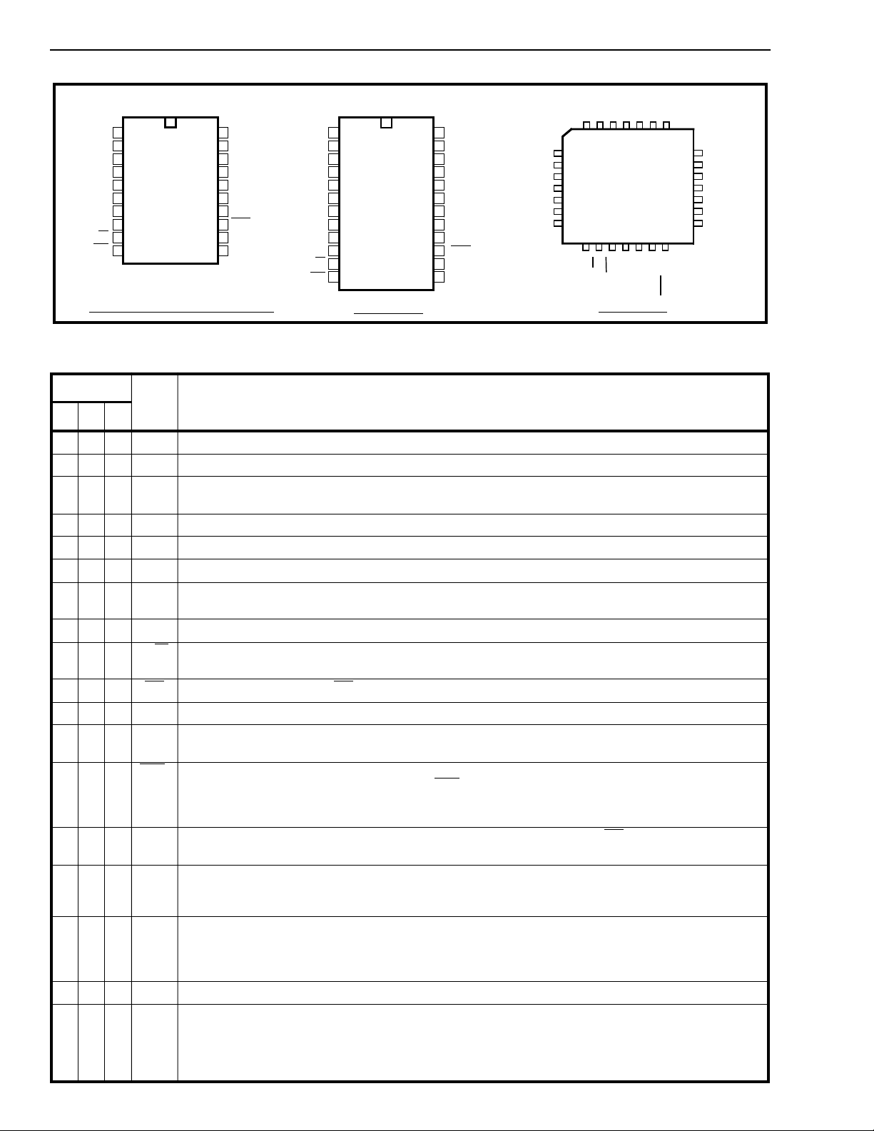
Ordering Information
MT8880CE/CE-1 20 Pin Plastic DIP
MT8880CC/CC-1 20 Pin Ceramic DIP
MT8880CS/CS-1 20 Pin SOIC
MT8880CN/C N-1 24 Pin SSO P
MT8880CP/CP-1 28 Pin Plastic LCC
-40°C to +85°C
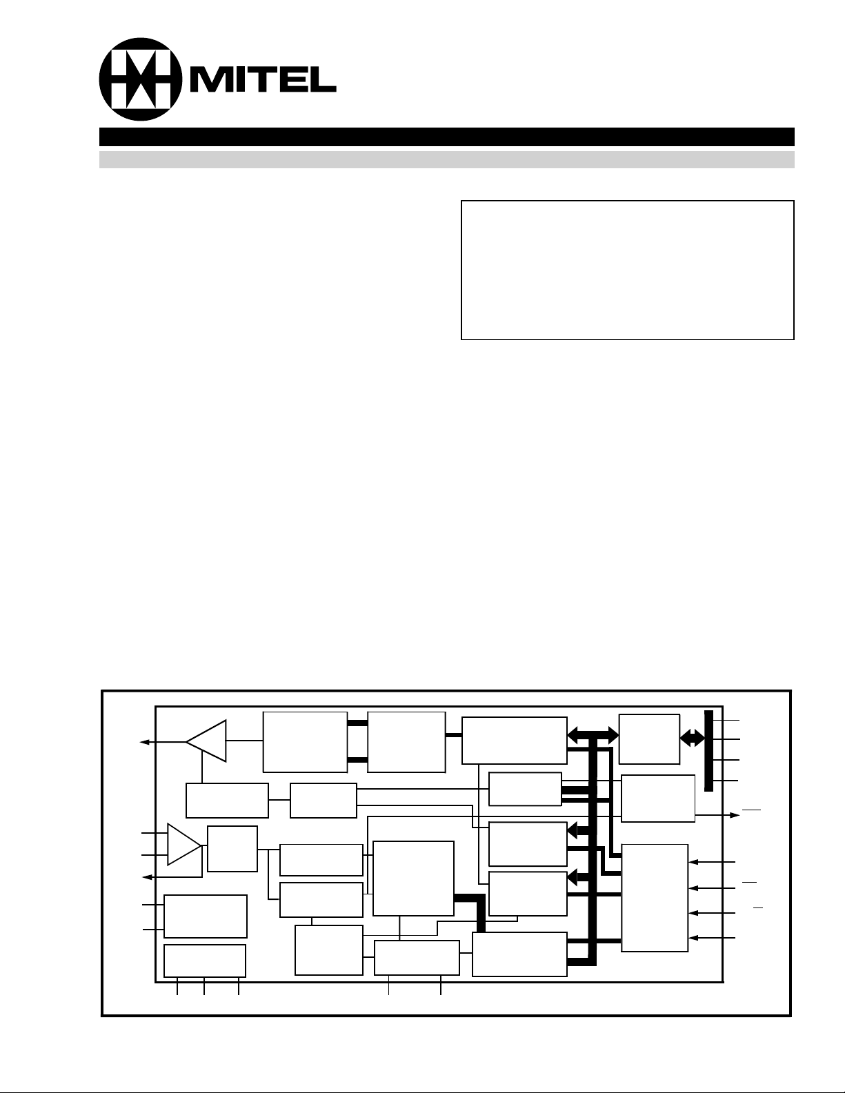
based upon the industry standard MT8870
monolithic DTMF receiver; the transmitter utilizes a
switched capacitor D/A converter for low distortion,
high accuracy DTMF signalling. Internal counters
provide a burst mode such that tone bursts can be
transmitted with precise timing. A call progress filter
can be selected allowing a microprocessor to
analyze call progress tones. A standard
microprocessor bus is provided and is directly
compatible with 6800 series microprocessors. The
MT8880C-1 is functionally identical to the MT8880C
except for the performance of the receiver section,
which is enhanced to accept and reject lower signal
level s.
The MT8880C/C-1 is a monolithic DTMF transceiver
with call progress filter. It is fabricated in Mitel’s
2
ISO
-CMOS technology, which provides low power
dissipation and high reliability. The DTMF receiver is
Row and
Column
Counters
Digital
Algorithm
and Code
Converter
Steering
Logic
ESt St/GT
TONE
IN+
IN-
GS
OSC1
OSC2
∑
Tone Burst
Gating Cct.
+
-
V
DDVRefVSS
Tone
Filter
Oscillator
Circuit
Bias
Circuit
D/A
Converters
Control
Logic
Dial
High Group
Filter
Low Group
Filter
Control
Logic
Figure 1 - Functional Block Diagram
Transmit Data
Register
Status
Register
Control
Register
A
Control
Register
B
Receive Data
Register
Data
Bus
Buffer
Inter rupt
Logi c
I/O
Control
D0
D1
D2
D3
IRQ
Φ2
CS
R/W
RS0
/CP
4-33
Page 2
MT8880C/MT8880C-1 ISO
1
IN+
2
IN-
3
GS
VRef
VSS
OSC1
OSC2
TONE
R/W
4
5
6
7
8
9
CS
10
20 PIN CERDIP/PLASTIC DIP/SOIC
20
19
18
17
16
15
14
13
12
11
VDD
St/GT
ESt
D3
D2
D1
D0
IRQ
Φ2
RS0
/CP
IN+
IN-
GS
VRef
VSS
OSC1
OSC2
NC
NC
TONE
R/W
CS
2
-CMOS
1
2
3
4
5
6
7
8
9
10
11
12
24 PIN SSOP
24
23
22
21
20
19
18
17
16
15
14
13
VDD
St/GT
ESt
D3
D2
D1
D0
NC
NC
IRQ
Φ2
RS0
/CP
NC
VRef
VSS
OSC1
OSC2
NC
NC
5
6
7
8
9
10
11
S
G
4
2
1
E
N
O
T
T
D
G
+
-
C
N
3
3
1
W
/
R
28 PIN PLCC
/
t
D
N
N
I
S
V
I
2
1
8
2
•
4
5
7
6
1
1
1
1
0
S
C
S
C
N
R
T
S
E
7
6
2
2
NC
25
NC
24
NC
23
D3
22
D2
21
D1
20
19
D0
8
1
2
P
Φ
C
/
Q
R
I
Figure 2 - Pin Connections
Pin Description
Pin #
20 24 28
1 1 1 IN+ Non-inverting op-amp input.
2 2 2 IN- Inverting op-amp input.
334 GSGain Select. Give s access to output of front end differential am plif ier for connection of
446V
557V
6 6 8 OSC1 DTMF clock/oscillator input.
7 7 9 OSC2 Clock output. A 3.579545 MHz crystal connected between OSC1 and OSC2 com plet es the
81012TONETone output (DTMF or single tone).
91113R/W
10 12 14 CS
11 13 15 RS0 Register Select input. See register decode table. TTL compatible.
12 14 17 Φ2 System Cloc k input . TTL co mpa tib le. N.B. Φ2 clock input need not be active when the
13 15 18 IRQ
14-1718-2119-22D0-D3 Microprocessor Data Bus (TTL compatible). High impedance when CS
Name Description
feedback resistor.
Reference Voltage output, nominally VDD/2 is used to bias inputs at mid-rail (see Fig. 13).
Ref
Ground input (0V).
SS
internal oscillator circuit. Leave open circuit when OS C1 is clock input.
Read/Write input. Cont ro ls the directi on of data transf er to and from the MPU an d the
transceiver registers. TTL compa tible.
Chip Select, TT L input (CS=0 t o select the chip).
device is not being accessed.
/CPInterrupt Request to MPU (open drain out put ). Also, when call progress (CP) mode has
been selected and interrupt enabled the IRQ/CP pin will output a rectangular wave signal
representative of the input signal applied at the input op-amp. The input signal must be within
the bandwidth limits of the call progress filter. See Figure 8.
= 1 or Φ2 is low.
18 22 26 ESt Early Steering outp ut. Presents a logic high once the digi tal algorit hm has detected a valid
tone pair (signal condition). Any momentary loss of signal condition will cause ESt to return to
a logic low.
19 23 27 St/GT Steering Input/Guard Time output (bidirection al). A voltage greater tha n V
causes the device to register the detected tone pair and upda te the output latch. A voltage
20 24 28 V
8,9
3,5,
16,
10,
17
11,
16,
23-
25
4-34
less than V
external steering time-constant; its state is a function of ESt and the voltage on St.
Positive power supply input (+5V typical).
DD
NC No Connect ion.
frees the device to accept a new tone pair. The GT output acts to reset the
TSt
detected at St
TSt
Page 3
ISO
Functional Description
The MT8880C/C-1 Integrated DTMF Transceiver
architecture consists of a high performance DTMF
receiver with internal gain setting amplifier and a
DTMF generator which employs a burst counter such
that precise tone bursts and pauses can be
synthesized. A call progress mode can be selected
such that frequencies within the specified passband
can be detected. A standard microprocessor
interface allows access to an internal status register,
two control registers and two data registers.
Input Configuration
2
-CMOS MT8880C/MT8880C-1
C1
C2
R1
R4
R3
R5
R2
IN+
IN-
GS
V
Ref
The input arrangement of the MT8880C/C-1 provides
a differential-input operational amplifier as well as a
bias sou rce (V
V
/2. Provision is made for connection of a
DD
) which is used to bias the inputs at
Ref
feedback resistor to the op-amp output (GS) for
adjustment of gain. In a single-ended configuration,
the input pins are connected as shown in Figure 3.
Figure 4 shows the necessary connections for a
differential input configuration.
IN+
C
VOLTAGE GAIN
(A
) = RF / R
V
IN
R
IN
R
F
IN-
GS
V
Ref
MT8880C/C-1
Figure 3 - Single-Ended Input Configuration
Receiver Se ction
Separation of the low and high group tones is
achieved by applying the DTMF signal to the inputs
of two sixth-order switched capacitor bandpass
filters, the bandwidths of which correspond to the low
and high group frequencies (see Fig. 7). These filters
also incorporate notches at 350 Hz and 440 Hz for
exceptional dial tone rejection. Each filter output is
followed by a single order switched capacitor filter
section which smooths the signals prior to limiting.
Limiting is performed by high-gain comparators
MT8880C/C-1
DIFFERENTIAL INPUT AMPLIFIER
C1 = C2 = 10 nF
R1 = R4 = R5 = 100 kΩ
R2 = 60kΩ, R3 = 37.5 kΩ
R3 = (R2R5)/(R2 + R5)
VOLTAGE GAIN
diff) = R5/R1
(A
V
INPUT IMPEDANCE
(Z
diff) = 2 R12 + (1/ωC)
IN
2
Figure 4 - Differential Input Configuration
which are provided with hysteresis to prevent
detection of unwanted low-level signals. The outputs
of the comparators provide full rail logic swings at
the frequencies of the incoming DTMF signals.
Following the filter section is a decoder employing
digital counting techniques to determine the
frequencies of the incoming tones and to verify that
they correspond to standard DTMF frequencies. A
complex averaging algorithm protects against tone
simulation by extraneous signals such as voice while
providing tolerance to small frequency deviations
and variations. This averaging algorithm has been
developed to ensure an optimum combination of
immunity to talk-off and tolerance to the presence of
interfering frequencies (third tones) and noise. When
the detector recognizes the presence of two valid
tones (this is referred to as the “signal condition” in
some industry specifications) the “Early Steering”
(ESt) output will go to an active state. Any
subsequent loss of signal condition will cause ESt to
assume an inactive s tate .
4-35
Page 4
MT8880C/MT8880C-1 ISO
2
-CMOS
Steering Circuit
Before registration of a decoded tone pair, the
receiver checks for a valid signal duration (referred
to as character recognition condition). This check is
performed by an external RC time constant driven by
ESt. A logic high on ESt causes v
rise as the capacitor discharges. Provided that the
signal condition is maintained (ESt remains high) for
the validation period (t
(V
) of the steering logic to register the tone pair,
TSt
), vc reaches the threshold
GTP
latching its corresponding 4-bit code (see Figure 7)
into the Receive D ata Regist er. At this point t he GT
output is activated and drives v
continues to drive high as long as ESt remains high.
Finally, after a short de lay to a ll ow th e o ut put latch to
settle, the delayed steering output flag goes high,
signalling that a received tone pair has been
registered. The status of the delayed steering flag
can be monitored by checking the appropriate bit in
the status register. If Interrupt mode has been
selected, the IRQ
/CP pin will pull low when the
delayed steering f l ag is activ e.
(see Figure 5) to
c
to VDD. GT
c
Guard Time Adjustment
The simple steering circuit shown in Figure 5 is
adequate for most applications. Component values
are chosen according to the formula:
t
= tDP+t
REC
tID=tDA+t
The value of tDP is a device parameter (see AC
Electrical Characteristics) and t
signal duration to be recognized by the receiver. A
value for C1 of 0.1 µF is recommended for most
applications, leaving R1 to be selected by the
designer. Different steering arrangements may be
used to select independently the guard times for tone
present (t
) and tone absent (t
GTP
necessary to meet system specifications which place
both accept and reject limits on both tone duration
and interdigital pause. Guard time adjustment also
allows the designer to tailor system parameters such
as talk off and noise immunity.
GTP
GTA
is the minimum
REC
). This may be
GTA
The contents of the output latch are updated on an
active delayed steering transition. This data is
presented to the four bit bidirectional data bus when
the Receive Data Register is read. The steering
circuit works in reverse to validate the interdigit
pause between signals. Thus, as well as rejecting
signals too short to be considered valid, the receiver
will tolerate signal interruptions (drop out) too short
to be considered a valid pause. This facility, together
with the capability of selecting the steering time
constants externally, allows the designer to tailor
performance to meet a wide variety of system
requirements.
V
DD
V
DD
St/GT
ESt
R1
C1
Vc
V
DD
St/GT
ESt
V
DD
St/GT
R1
= (RPC1) In [VDD / (VDD-V
t
GTP
t
= (R1C1) In (VDD/V
GTA
R
= (R1R2) / (R1 + R2)
P
C1
R2
a) decreasing tGTP; (tGTP < tGTA)
= (R1C1) In [VDD / (VDD-V
t
GTP
= (RpC1) In (VDD/V
t
GTA
= (R1R2) / (R1 + R2)
R
P
C1
TSt
TSt
TSt
TSt
)]
)
)
)
MT8880C/C-1
4-36
t
= (R1C1) In (VDD / V
GTA
t
= (R1C1) In [VDD / (VDD-V
GTP
TSt
)
Figure 5 - Basic Steering Circuit
TSt
R1
)]
ESt
R2
b) decreasing tGTA; (tGTP > tGTA)
Figure 6 - Guard Time Adjustment
Page 5
ISO
AAAA
AAAA
A
A
A
A
AAAA
A
A
A
AA
2
-CMOS MT8880C/MT8880C-1
Increas ing t
improves talk-off performance since
REC
it reduces the probability that tones simulated by
speech will maintain a valid signal condition long
enough to be registered. Alternatively, a relatively
short t
with a long tDO would be appropriate for
REC
extremely noisy environments where fast acquisition
time and immunity to tone drop-outs are required.
Design information for guard time adjustment is
shown in Figure 6. The receiver timing is shown in
Figure 9 with a description of the events in Figure 11.
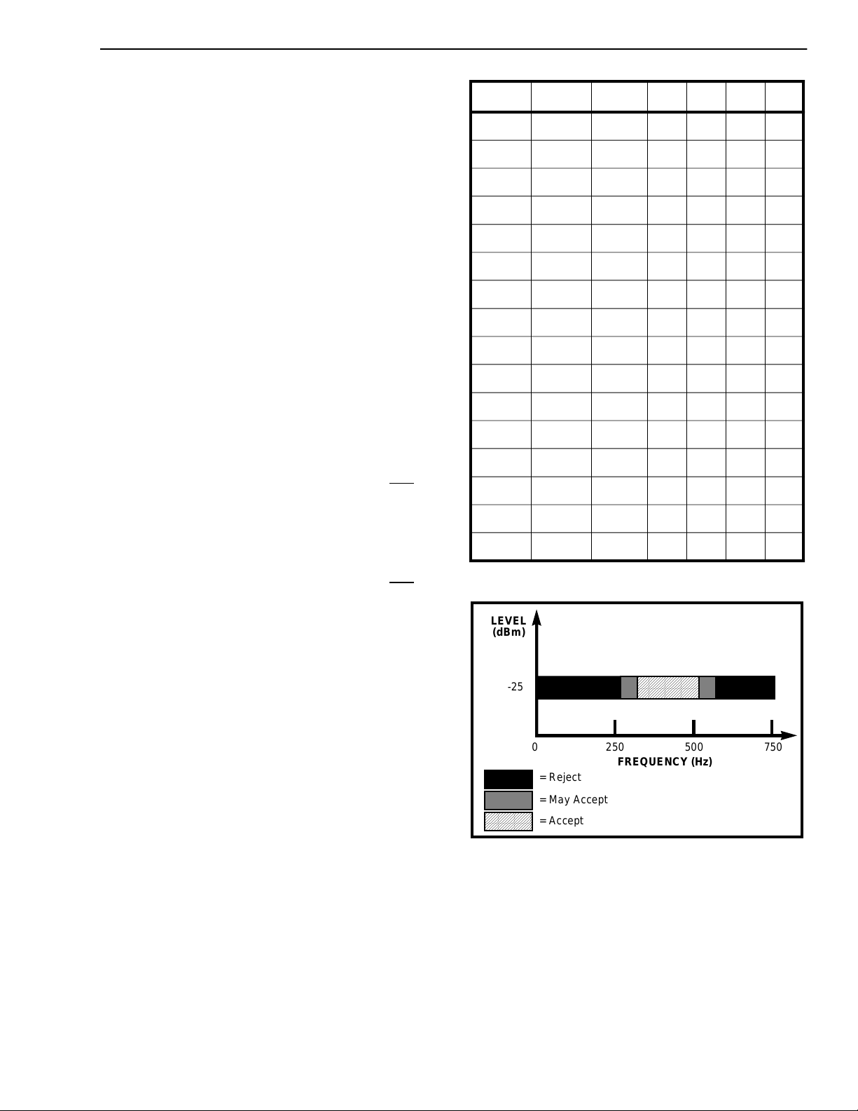
Call Progress Filter
A call progress mode, using the MT8880C/C-1, can
be selected allowing the detection of various tones
which identify the progress of a telephone call on the
network. The call progress tone input and DTMF
input are common, however, call progress tones can
only be detected when CP mode has been selected.
DTMF signals cannot be detected if CP mode has
been selected (see Table 5). Figure 8 indicates the
useful detect bandwidth of the call progress filter.
Frequencies presented to the input, which are within
the ‘accept’ bandwidth limits of the filter, are hardlimited by a high gain comparator with the IRQ
/CP
pin serving as the output. The squarewave output
obtained from the schmitt trigger can be analyzed by
a microprocessor or counter arrangement to
determine the nature of the call progress tone being
detected. Frequencies which are in the ‘reject’ area
will not be detected and consequently the IRQ
/CP
pin will remain low.
DTMF Generat or
F
LOW
F
HIGH
DIGIT D
D
D
3
2
D
1
0
6971209 1 0001
6971336 2 0010
6971477 3 0011
7701209 4 0100
7701336 5 0101
7701477 6 0110
8521209 7 0111
8521336 8 1000
8521477 9 1001
9411336 0 1010
9411209 * 1011
9411477 # 1100
6971633 A 1101
7701633 B 1110
8521633 C 1111
9411633 D 0000
0= LOGIC LOW, 1= LOGIC HIGH
Figure 7 - Functional Encode/Decode Table
LEVEL
(dBm)
The DTMF transmitter employed in the MT8880C/C1 is capable of generating all sixteen standard DTMF
tone pairs with low distortion and high accuracy. All
frequencies are derived from an external 3.579545
MHz crystal. The sinusoidal waveforms for the
individual tones are digitally synthesized using row
and column programmable dividers and switched
capacitor D/A converters. The row and column tones
are mixed and filtered providing a DTMF signal with
low total harmonic distortion and high accuracy. To
specify a DTMF signal, data conforming to the
encoding format shown in Figure 7 must be written to
the transmit Data Register. Note that this is the same
as the receiver output code. The individual tones
which are generated (f
LOW
and f
) are referred to
HIGH
as Low Group and High Group tones. As seen from
the table, the low group frequencies are 697, 770,
852 and 941 Hz. The high group frequencies are
1209, 1336, 1477 and 1633 Hz. Typically, the high
group to low group amplitude ratio (pre-emphasis) is
2dB to compensate for high group attenuation on
long loops.
AAA
AAAA
AAAA
AAA
AAAA
-25
AAA
AAA
AAAA
AAAA
AAAA
AAAA
AAAA
0 250 500 750
FREQUENCY (Hz)
= Reject
= May Accept
AAA
AAAA
A
AAA
AAAA
A
AAAA
= Accept
A
AAA
Figure 8 - Call Progress Response
The period of each tone consists of 32 equal time
segments. The period of a tone is controlled by
varying the length of these time segments. During
write operations to the Transmit Data Register the 4
bit data on the bus is latched and converted to 2 of 8
coding for use by the programmable divider circuitry.
This code is used to specify a time segment length
which will ultimately determine the frequency of the
tone. When the divider reaches the appropriate
count, as determined by the input code, a reset pulse
is issued and the counter starts again. The number
4-37
Page 6
MT8880C/MT8880C-1 ISO
2
-CMOS
EVENTS
V
in
ESt
St/GT
RX
-RX
0
b3
b2
Read
Status
Register
/CP
IRQ
ABCDEF
t
t
REC
t
DP
3
DECODED TONE # (n-1)
REC
TONE #n
t
GTP
t
PStRX
t
PStb3
t
ID
# n
t
DO
TONE
#n + 1
t
DA
t
GTA
TONE
#n + 1
# (n + 1)
V
TSt
Figure 9 - R ece iver Tim ing Diag ram
of time segments is fixed at 32, however, by varying
the segment length as described above the tone
output signal frequency will be varied. The divider
output clocks another counter which addresses the
sinewave lookup ROM.
The lookup table contains codes which are used by
the switched capacitor D/A converter to obtain
discrete and highly accurate DC voltage levels. Two
identical circuits are employed to produce row and
column tones which are then mixed using a low
noise summing amplifier. The oscillator described
needs no “start-up” time as in other DTMF
generators since the crystal oscillator is running
continuously thus providing a high degree of tone
burst accuracy. A bandwidth limiting filter is
incorporated and serves to attenuate distortion
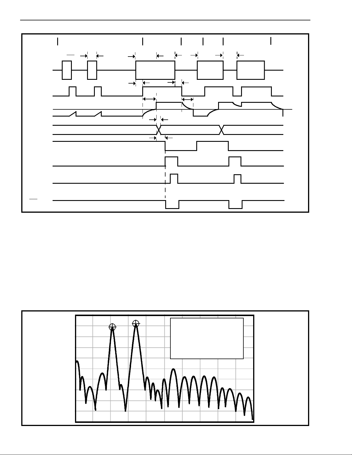
products above 8 kHz. It can be seen from Figure 10
that the distortion products are very low in amplitude.
Scaling Information
10 dB/Div
Start Frequency = 0 Hz
Stop Frequency = 3400 Hz
Marker Frequency = 697 Hz and
1209 Hz
4-38
Figure 10 - Spectrum Plot
Page 7

ISO
2
-CMOS MT8880C/MT8880C-1
Burst Mode
In certain telephony applications it is required that
DTMF signals being generated are of a specific
duration determined either by the particular
application or by any one of the exchange trans mitter
specifications currently existing. Standard DTMF
signal timing can be accomplished by making use of
the Burst Mode. The transmitter is capable of issuing
symmetric bursts/pauses of predetermined duration.
This burst/pause duration is 51 ms±1 ms which is a
standard interval for autodialer and central office
applications. After the burst/pause has been issued,
the appropriate bit is set in the Status Register
indicating that the transmitter is ready for more data.
The timing described above is available when DTMF
mode has been selected. However, when CP mode
(Call Progress mode) is selected, a second burst/
pause time of 102 ms ±2 ms is available. This
extended interval is useful when precise tone bursts
of longer than 51 ms duration and 51 ms pause are
desired. Note that when CP mode and Burst mode
have been selected, DTMF tones may be transmitted
only and
In applications where a non-standard burst/pause
duration is required, burst mode must be disabled
not
received .
and the transmitter gated on and off by an external
hardware o r software t im e r.
Single Tone Generation
A single tone mode is available whereby individual
tones from the low group or high group can be
generated. This mode can be used for DTMF test
equipment applications, acknowledgment tone
generation and distortion measurements. Refer to
Control Register B description for details.
Distortion Calculations
The MT8880C/C-1 is capable of producing precise
tone bursts with minimal error in frequency (see
Table 1). The internal summing amplifier is followed
by a first-order lowpass switched capacitor filter to
minimize harmonic components and intermodulation
products. The total harmonic distortion for a
tone
can be calculated using Equation 1, which is the
ratio of the total power of all the extraneous
frequencies to the power of the fundamental
frequency expressed as a percentage. The Fourier
components of the tone output correspond to V
V
as measured on the output waveform. The total
nf
harmonic distortion for a
dual tone
can be calculated
single
....
2f
EXPLANATION OF EVENTS
A) TONE BURSTS DETECTED, TONE DURATION INVALID, RX DATA REGISTER NOT UPDATED.
B) TONE #n DETECTED, TONE DURATION VALID, TONE DECODED AND LATCHED IN RX DATA REGISTER.
C) END OF TONE #n DETECTED, TONE ABSE N T DURATION VALID, IN FOR MATION IN R X DATA REGISTER
D) TONE #n+1 DETECTED, TONE DURATION VALID, TONE DECODED AND LATCHED IN RX DATA REGISTER.
E) ACCEPTABLE DROPOUT OF TONE #n+1, TONE ABSENT DURATION INVALID, DATA REMAINS UNCHANGED.
F) EN D O F TONE # n+1 D ETEC TED, TONE ABSEN T DURATION VALID, INFO RM ATION IN RX D ATA REG IST ER
EXPLANATION OF SYMBOLS
V
ESt EARLY STEERING OUTPUT. INDICATES DETECTION OF VALID TONE FREQUENCIES.
St/GT STEERING INPUT/GUARD TIME OUTPUT. DRIVES EXTERNAL RC TIMING CIRCUIT.
RX
b3 DELAYED STEERING. INDICATES THAT VALID FREQUENC IES HAVE BEEN PRE SEN T/ ABSE NT F OR THE
b2 INDICATES THAT VALID DATA IS IN THE RECEIVE DATA REGISTER. THE B IT IS CL EARED AFTER THE STATUS
IRQ
t
REC
t
REC
t
ID
t
DO
t
DP
t
DA
t
GTP
t
GTA
RETAINED UNTIL NEXT VALID TONE PAIR.
RETAINED UNTIL NEXT VALID TONE PAIR.
DTMF COM PO SIT E INPUT SIGNAL.
in
-RX34-BIT DECODED DATA IN RECEIVE DATA REGISTER
0
REQUIRED GUARD TIME THUS CONSTITUTING A VALID SIGNAL. ACTIVE LOW FOR THE DURATION OF A
VA LID DTMF SI GNAL.
REGISTER IS R EA D.
/CP INTERRUPT IS ACTIVE INDICATING THAT NEW DATA IS IN THE RX DATA REGISTER. THE INTERRUPT IS
CLEARED AFTER THE STATUS REGISTER IS READ.
MAXIMUM DTMF SIGNAL DURATION NOT DETECTED AS VALID.
MINIMUM DTMF SIGNAL DURATION REQUIRED FOR VALID RECOGNITION.
MINIMUM TIME BETWEEN VALID SEQUENTIAL DTMF SIGNALS.
MAXIMUM ALLOWABLE DROPOUT DURING VALID DTMF SIGNAL.
TIME TO DETECT VALID FREQU ENC IES PRESENT.
TIME TO DETECT VALID FREQU ENC IES ABS EN T.
GUARD TIME, TONE PRES ENT.
GUARD TIME, TONE ABSEN T.
Figure 11 - Description of Timing Events
4-39
Page 8

MT8880C/MT8880C-1 ISO
2
2
+ V
3f
V
fundamental
2
THD(%) = 100
V
+ V
2f
Equation 1. THD (%) For a Single Tone
2
V
2
+ V
2L
3L
2
V
+ .. V
3H
+ .... V
2
nH
2
+ V
nL
4f
+ .... V
2
+ V
2
IMD
2H
2
nf
+
2
-CMOS
Maximum Series Resistance:150 ohms
Maximum Drive Level: 2mW
e.g. CTS Knights MP036S
Toyocom TQC-203-A-9S
A number of MT8880C/C-1 devices can be
connected as shown in Figure 12 such that only one
crystal is required. Alternatively, the OSC1 inputs on
all devices can be driven from a TTL buffer with the
OSC2 outputs left unconnected.
THD (%) = 100
2
2
V
+ V
L
H
Equation 2. THD (% ) For a Dual Tone
OUTPUT FREQUENCY
ACTIVE
INPUT
SPECIFIED ACTUAL
(Hz)
%ERROR
L1 697 699.1 +0.30
L2 770 766.2 -0.49
L3 852 847.4 -0.54
L4 941 948.0 +0.74
H1 1209 1215.9 +0.57
H2 1336 1331.7 -0.32
H3 1477 1471.9 -0.35
H4 1633 1645.0 +0.73
Table 1. Actual Frequencies Versus Standard
Requirements
using Equation 2. V
group amplitude and high group amplitude,
respectively, and V
and VH correspond to the low
L
2
is the sum of all the
IMD
intermodulation components. The internal switchedcapacitor filter following the D/A converter keeps
distortion products down to a very low level as
shown in Figure 10.
DTMF Clo ck Ci rcuit
The internal clock circuit is completed with the
addition of a standard television colour burst crystal.
The crystal specification is as follows:
Frequency: 3.579545 MHz
Frequency Tolerance:
Resonance Mode: Parallel
Load Capacitance: 18pF
±0.1%
MT8880C/C-1
OSC1 OSC2
3.579545 MHz
MT8880C/C-1
OSC1 OSC2
MT8880C/C-1
OSC1 OSC2
Figure 12 - Common Crystal Connection
Microprocessor Interfa ce
The MT8880C/C-1 employs a microprocessor
interface which allows precise control of transmitter
and receiver functions. There are five internal
registers associated with the microprocessor
interface which can be subdivided into three
categorie s, i.e., dat a t ran sfe r, transce i ver control a nd
transceiver status. There are two registers
associated with data transfer operations.
The Receive Data Register contains the output code
of the last valid DTMF tone pair to be decoded and is
a read only register. The data entered in the Transmit
Data Register will determine which tone pair is to be
generated (see Figure 7 for coding details). Data can
only be written to the transmit register. Transceiver
control is accomplished with two Control Registers
(CRA and CRB) which occupy the same address
space. A write operation to CRB can be executed by
setting the appropriate bit in CRA. The following
write operation to the same address will then be
directed to CRB and subsequent write cycles will
then be directed back to CRA. A software reset must
be included at the beginning of all programs to
initialize the control and status registers after power
up or power reset (see Figure 16). Refer to Tables 3,
4, 5 and 6 for details concerning the Control
Registe r s . Th e IRQ
that it will provide an interrupt request signal upon
validation of DTMF signals or when the transmitter is
ready for more data (Burst mode only). The IRQ
pin is configured as an open drain output device and
as such requires a pull-up resistor (see Figure 13).
/CP pin can be programmed such
/CP
4-40
Page 9

ISO
2
-CMOS MT8880C/MT8880C-1
RS0 R/W
0 0 Write to Transmit
0 1 Read from Receive
1 0 Write to Control
1 1 Read from Status
Table 2. Internal Register Functions
BIT NAME FUNCTION DESCRIPTION
b0 TOUT TONE OUTPUT A logic ‘1’ enables the tone output. This function can be
b1 CP/DTMF MO DE CONTROL In DTMF mod e (logic ‘0’) the device is capabl e of generating
FUNCTION
Data Register
Data Register
Register
Register
b3 b2 b1 b0
RSEL IRQ CP/DTMF
Table 3. CRA Bit Po sitions
b3 b2 b1 b0
C/R
implemented in either the bu r st mode or non-burst mode
and receiving Dual Tone Multi-Frequency signals. When the
CP (Call Progress) mode is selected (logic ‘1’) a 6th order
bandpass filter is enabled to allow call progress tones to be
detected. Call progress tones which are within the specified
bandwidth will be presented at the IRQ/CP pin in
rectangular wave format if the IRQ bit has been enabled
(b2=1). Also, when the CP mo de and BURS T m ode have bo th
been selected, the transmitter will issue DTMF signals with a
burst and pause of 102 ms (t yp) durat ion. T his signal duration
is twice that obtained from the DTMF transmitter if DTMF
mode had been selected. Note that DTMF signals cannot be
decoded when the CP mod e of operation has been select ed.
S/D TEST BURST
Table 4. CRB Bit Po sitions
TOUT
.
b2 IRQ INTERRUPT ENABLE A logic ‘1’ enables t he INTERRUPT mode. W hen this mode i s
active and the DTMF mode has been selected (b1=0) the IRQ
CP pin wi ll pull to a logic ‘0’ con dition when eithe r 1) a valid
DTMF signal has been received and has been present for the
guard time duration or 2) the transmitter is ready for more data
(BURST mode only).
b3 RS EL REGISTER SELE CT A logic ‘1’ selects C ontrol Register B on the next Write cycle to
the Control R egister address. Subsequent Write cy cles to the
Control Register are directed back to Control Register A.
Table 5. Control Register A Description
/
4-41
Page 10

MT8880C/MT8880C-1 ISO
BIT NAME FUNCTION DESCRIPTION
b0 BURST BURST MODE A logic ‘0’ enables the burst mode. When this mode is
2
-CMOS
selected, data corresponding to the desired DTM F tone pair
can be written to the Transmit Register resulting in a tone
burst of a specific duration (see AC Characteristics).
Subsequently, a pause of the same duration is induced.
Immediately following the pause, the Status Register is
updated indicating that the Transmit Register is ready for
further instructions an d an interrupt will be gen erated if the
interrupt mode has been enabled. Additionally, if call
progress (CP) mode has be en en abled, the burst and p ause
duration is increased by a factor of two. When the burst
mode is not selected (logic ‘1’) tone bursts of any desired
duration may be generated.
b1 TEST TEST MODE By enabling the test mode (logic’1’), the IRQ
present the delayed steering (inverted) signal from the DTMF
receiver. Refer to Figure 9 (b3 waveform) for details
concerning the output waveform. DTMF mode must be
selected (CRA b1=0) before test mode can be implemented.
b2 S/D
b3 C/R
BIT NAME STATUS FLAG SET STATUS FLAG CLE ARED
b0 IRQ Interrupt has occurred. Bit one (b1)
b1 TRANSMIT DATA
REGISTER EMPTY
(BURST MODE ONLY)
SINGLE /DUA L TONE
GENERATION
COLUMN/ROW TONES When used in conjunction with b2 (above) the transmitter
Ta ble 6. Control Register B Des cription
or bit two (b2) is set.
Pause duration has terminated
and transmitter is ready for new
data.
A logic ‘0’ will allow Dual Tone Multi-Frequency signals to be
produced. If single tone generation is enabled (logic ‘1’),
either row or column tones (low group or high group) can be
generated dependi ng on the stat e of b3 in Control Register
B.
can be made to generate single row or single column
frequencies. A logic ‘0’ will select row frequencies and a logic
‘1’ will select column frequencies.
Interrupt is inactive. Cleared after
Status Register is read.
Cleared after Status Register is
read or when in non-burst mode.
/CP pin will
b2 RECEIVE DATA
REGISTER FULL
b3 DELAYED
4-42
Valid data is in the Receive Data
Register.
STEERING Set upon the valid detection of the
absence of a DTMF signal.
Table 7. Sta tus Registe r Desc rip tion
Cleared after Status Register is
read.
Cleared upon the detection of a
valid DTMF signal.
Page 11

ISO
2
-CMOS MT8880C/MT8880C-1
V
DD
DTMF/CP
INPUT
DTMF
OUTPUT
Notes:
R1, R2 = 100 kΩ 1%
R3 = 374 Ω 1%
R4 = 3.3 kΩ 10%
RL = 10 k Ω (min.)
C1 = 100 nF 5%
C2 = 100 nF 5%
C3 = 100 nF 10%*
C4 = 10 nF 10%
X-tal = 3.579545 MHz
C1
R1
C4
R2
X-tal
R
L
MT8880C/C-1
St/GT
IRQ
VDD
ESt
D3
D2
D1
D0
/CP
Φ2
RS0
C2
R3
IN+
INGS
VRef
VSS
OSC1
OSC2
TONE
R/W
CS
* Microprocessor based systems can inject undesira ble noise into
the supply rails. The performance of the MT8880 can be optimized
by keeping noise on the supply rails to a minimum. The decoupling
capacitor (C3) should be connecte d close to the device and ground
loops should be avoided.
C3
R4
To µP
or µC
TEST POINT
130 pF
Figure 13 - Application Circuit (Single-Ended Input)
MMD6150
(or equivalent)
24 kΩ
5.0 VDC
2.4 kΩ
MMD7000
(or equivalent)
TEST POINT
Figure 14 - Te st Circuit
Test load for IRQ
5.0 VDC
3 kΩ
70 pF
/CP pinTest load for D0-D3 pins
4-43
Page 12

MT8880C/MT8880C-1 ISO
2
-CMOS
+5V
6802
IRQ
Address
Peripheral decode
VMA
R/W
E
Data
3.3k
MT8880C/C-1
IRQ
RS0
CS
R/W
Φ2
Data
Figure 15 - MT 88 80C/C-1 t o 68 02 Inte rfa ce
EXAMPLE 1: A software reset must be included at the beginning of all programs to initialize the control
registers after power up. The initialization procedure should be implemented 100ms after power up.
Description Control Data
RS0 R/W b3 b2 b1 b0
CS
1) Read Status Register 0 1 1 X X X X
2) Write to Control Register 0 1 0 0 0 0 0
3) Write to Control Register 0 1 0 0 0 0 0
4) Write to Control Register 0 1 0 1 0 0 0
5) Write to Control Register 0 1 0 0 0 0 0
6) Read Status Register 0 1 1 X X X X
EXAMPLE 2 : Transmit DTMF tones of 50 ms burst/50 ms pause and Receive DTMF Tones
Description
RS0 R/W b3 b2 b1 b0
CS
1) Write to Control Register A 0 1 0 1 1 0 1
(tone out, DTMF, IRQ
, Select C ontrol Registe r B)
2) Write to Control Register B 0 1 0 0 0 0 0
(burst mode)
3) Write to Transmit Data Register 0 0 0 0 1 1 1
(send a digit 7)
-------------------- ---------- --------
wait for an interrupt or poll Sta tus Register ----------- -----------------------------------
4) Read the Status Register 0 1 1 X X X X
-if bit 1 is set, the Tx is ready for the next tone, in which case...
Write to Transmit Register 0 0 0 0 1 0 1
(send a digit 5)
-if bit 2 is set, a DT MF tone ha s b ee n received, i n whi c h c a se....
Read th e Re cei v e Da ta R e gis te r 0 0 1 X X X X
-if both b its a r e set...
Read th e Re cei v e Da ta R e gis te r 0 0 1 X X X X
Write to Transmit D a ta R e gister 0 0 0 0 1 0 1
NOTE: IN THE TX BURST MODE, STATUS REGISTER BIT 1 WILL NOT BE SET UNTIL 100 ms (±2 ms) AFTER THE DATA IS
WRITTEN TO THE TX DATA REGISTER. IN EXTENDED BURST MODE THIS TIME WILL BE DOUBLED TO 200 ms (± 4 ms)
Figure 16 - Application Hints
4-44
.
Page 13

Absolute Maximum Ratings*
Parameter Symbol Min Max Units
ISO
2
-CMOS MT8880C/MT8880C-1
1 Powe r supply voltage V
DD-VSS
2 Voltage on any pin V
3 Cu rren t at any pin (E xcep t V
DD and VSS
)10mA
4 Storage tempera ture T
5 Package power dissipation P
* Exceeding these values may cause perman ent dama ge. Functi on al operati on under these co ndition s is not implie d.
Recommended Operating Conditions - Voltages are with respect to ground (V
Parameter Sym M in Typ
1 Positive power supply V
2 Operating temperature T
3 Crystal clock frequen cy f
‡ Typical figures are at 25 °C and for design aid only: not guaran teed an d not subject to productio n testi ng.
DC Electrical Characteristics
DD
O
CLK
†
- VSS=0 V.
Characteristi cs S ym M i n Typ
1
2 Operating supply current I
3 Power consumption P
4
5 Low level input voltage
6 Steering threshold voltage V
7
Operating supply voltage V
S
U
P
High level input voltage
I
(OSC1)
N
P
U
(OSC1)
T
S
Low level output voltag e
(OSC2) V
O
8 High level output voltage
U
T
(OSC2) V
P
9 Output leakage current
U
(IRQ) I
T
10 V
S
11 V
12
13 High level input voltage V
14 Input leakage current I
15
16 Sink current I
17
18 Sink current I
19
† Characteristics are over recommended operating conditions unless otherwise stated.
‡ Typical figures are at 25 °C, V
D
i
g
i
t
a
l
Data
Bus
ESt
and
St/Gt
IRQ/
CP
output voltage V
Ref
output resistance R
Ref
Low level input voltage V
Source current I
Source current I
Sink current I
=5V and for design aid only: not guaranteed and not subject to production testing.
DD
4.75 5.00 5.25 V
-40 +85 °C
3.575965 3.579545 3.583124 MHz
4.75 5.0 5.25 V
C
3.5 V
2.2 2. 3 2.5 V VDD=5V
4.9 V
2.4 2.5 2.6 V No load, VDD=5V
IL
IH
2.0 V
-1.4 -6.6 mA VOH=2.4V
2.0 4. 0 mA VOL=0.4V
-0.5 -3.0 mA VOH=4.6V
24 mAV
416 mAVOL=0.4V
V
V
OLO
OHO
DD
DD
IHO
ILO
TSt
OZ
Ref
OR
IZ
OH
OL
OH
OL
OL
V
DD
I
ST
D
‡
‡
VSS-0.3 VDD+0.3 V
-65 +150 °C
) unless otherwise stated.
SS
Max Units Test Conditio ns
Max Uni ts Test Co ndi tions
7.0 11 mA
57.8 mW
1.5 V
No load
0.1 V
No load
VDD=5 V
110µAVOH=2.4 V
1.3 kΩ
0.8 V
10 µAVIN=VSS to V
6V
1000 mW
DD
=0.4V
OL
4-45
Page 14

MT8880C/MT8880C-1 ISO
2
-CMOS
Electrical Characteristics
Gain Setting Amplifier - Voltages are with respect to ground (V
Characteristi cs Sym Min Typ
) unless otherwise stated, VSS= 0 V, VDD=5V, TO=25°C.
SS
‡
Max Uni ts Test Con ditio ns
1 Input leakage current I
2 Input resistance R
3 Inpu t offset voltage V
IN
IN
OS
±100 nA VSS ≤ VIN ≤ V
10 M Ω
25 mV
4 Power supply rejection PSRR 60 dB 1 kHz
5 Comm on m ode reject ion CM RR 60 dB 0.75V ≤ V
6 DC open loop volta ge gain A
VOL
65 dB
7 Unity gain bandwidth BW 1.5 MHz
8 Output voltage swing V
9 Allowable capacitive load (GS) C
10 Allowabl e resistive load (GS ) R
11 Common mode range V
‡ Ty p ical figures are at 25°C and for design aid only: not guarantee d and not subject to product ion testi ng.
O
L
L
CM
MT8880C-1 AC Electrical Characteristics† - Voltages are with respect to ground (V
4.5 V
100 pF
50 kΩ
3.0 V
pp
pp
RL ≥ 100 kΩ to V
No Load
) unless otherwise stated.
SS
Characteristics Sym Min Typ Max Units Notes*
Valid input signal levels
(each tone of composite
1
signal)
R
X
-31 dBm 1,2,3,5,6,9
21.8 mV
RMS
1,2,3,5,6,9
+1 dBm 1,2,3,5,6,9
869 mV
RMS
1,2,3,5,6,9
2 Input Signal Level Reje ct -37 dBm 1,2,3,5,6 ,9
1,2,3,5,6,9
† Characteristics are over recommended temperature and at V
MT8880C AC Electrical Characteristics
Characteristics Sym Mi n Typ
10.9 mV
=5V, using the test circuit shown in Figure 13.
DD
†
- Voltages are with respect to ground (V
‡
Max Units Notes*
RMS
) unless otherwise stated.
SS
≤ 4.25V
IN
DD
SS
-29 dBm 1,2,3,5,6,9
V alid Input signal levels
R
1
† Characteristics are over recommended operating conditions (unless otherwise stated) using the test circuit shown in Figure 13.
(each tone of composite
X
signal)
AC Electrical Characteristics† - Voltages are with respect to ground (V
Characteristics Sym Min T yp
1
Positive twist accept 8 dB 2,3,6,9
27.5 mV
+1 dBm 1,2,3,5,6,9
869 mV
) unless otherwise stated. fC=3.57954 5 MHz.
SS
‡
Max Units Notes*
RMS
RMS
1,2,3,5,6,9
1,2,3,5,6,9
2 Negative twist accept 8 dB 2,3,6,9
3 Freq. deviation accept ±1.5%±2Hz 2,3,5,9
R
4 Freq. deviation reject ±3.5% 2,3,5
X
5 Third tone tolerance -16 dB 2 ,3,4,5,9 ,10
6 Noise tolerance -12 dB 2,3,4,5,7,9,10
7 Dial tone tolerance 22 dB 2,3,4, 5,8 ,9, 11
† Characteristics are over recommended operating conditions unless otherwise stated.
‡ Typical figures are at 25°C, V
* See “Notes” following AC Electrical Chara cteri sti cs Tables.
4-46
= 5V, and for design aid only: not guaranteed and not subject to production testing.
DD
Page 15

ISO
2
-CMOS MT8880C/MT8880C-1
AC Electrical Characteristics
Characteristics Sym Min Typ
1 Lower freq. (ACCEPT) f
2 Upper freq. (ACCEPT) f
3 Lower freq. (REJECT) f
4 Upper freq. (REJECT) f
5 Call progress tone detect level
†
- Call Progress - Vol tag es are with respe ct to ground (V
‡
Max Units Notes*
LA
HA
LR
HR
320 Hz @ -25 dBm
510 Hz @ -25 dBm
290 Hz @ -25 dBm
540 Hz @ -25 dBm
-30 dBm
) unless otherwise stated.
SS
(total power)
† Characteristics are over recommended operating conditions unless otherwise stated
‡ Typical figures are at 25°C, V
* See “Notes” AC Electrical Characteristics Tables
AC Electrical Characteristics† - Voltages are with respect to ground (V
= 5V, and for design aid only: not guaranteed and not subject to production testing
DD
) unless otherwise stated.
SS
Characteristics Sym Min Typ‡Max Units Conditions
1
2 Tone absent detect time t
3 Tone duration accept t
4 Tone duration reject t
5 Interdigit pause accept t
6 Interdigit pause reject t
7 Delay St to b3 t
8 Delay St to RX
9
10 Tone pause duration t
11 Tone burst duration (extended) t
12 Tone pause duration (extended) t
13
14 Low group output level V
15 Pre-emphasis dB
16 O utput dist orti on (Sin gle Tone) TH D -35 dB 25 kHz Band widt h
17 Frequen cy deviation f
18 Out put loa d resistan ce R
19
20 Φ2 high pulse width t
21 Φ2 low pulse width t
22 Φ2 rise and fall time
23 Address, R/W
24 Address, R/W
25 Da ta hold time (read) t
26 Φ2 to valid data delay (read) t
27 Data setup time (write) t
Tone present det ect t im e t
R
X
-RX
0
3
Tone burst durat ion t
T
X
High group output level V
T
O
N
E
O
U
T
Φ2 cycle period t
M
P
U
I
N
T
E
R
F
A
C
E
hold time t
setup time (before Φ2) t
DP
DA
REC
REC
ID
DO
PStb3
t
PStRX
BST
PS
BSTE
PSE
HOUT
LOUT
P
D
LT
CYC
CH
CL
tR, tF
AH,tRWH
AS,tRWS
DHR
DDR
DSW
3 1114msNote 12
0.5 4 8. 5 m s Note 12
40 ms User adjust able
20 ms User adjustable
40 ms User adjust able
20 ms User adjustable
13 µs
8 µs
50 52 ms DTMF mod e
50 52 ms DTMF mod e
100 104 ms Call Progress mode
100 104 ms Call Progress mode
-6.1 -2.1 dBm RL=10kΩ
-8.1 -4.1 dBm RL=10kΩ
23dBR
=10kΩ
L
=10kΩ
R
L
±0.7 ±1.5 % fC=3.579545 MHz
10 50 kΩ
250 ns
115 ns
110 ns
25 ns
26 ns
23 ns
22 ns *
100 ns 200 pF load
45 ns
#
#
#
#
4-47
Page 16

MT8880C/MT8880C-1 ISO
2
-CMOS
AC Electrical Characteristics† (Cont‘d) - Voltages are with respect to ground (V
Characteristics Sym Min Typ
28 Data hold time (write) t
29 Input Capacitance (data bus) C
30 Output Capacitance (IRQ
31
32 Clock input rise time t
33 Clock input duty cycle t
34 Clock input duty cycle DC
35 Capacitive load (OSC2) C
† Timing is over recommended temperature & power supply voltages.
‡ Ty p ical figures are at 25°C and for design aid only: not guarantee d and not subject to product ion testi ng.
* The data bus output buffers are no longer sourcing or sinking current by t
#
See Figure 6 regarding guard time adjustment.
NOTES: 1) dB m =d ec ib el s ab ov e or be low a refe r e nc e po w er of 1 m W into a 60 0 o hm load.
Crystal/clock frequency f
D
T
M
F
C
L
K
2) Digit sequence co nsists of all 16 DTMF tones.
3) Tone duration=40 ms. Tone pause=40 ms.
4) Nominal DTMF freque nc ie s are use d .
5) Both tone s in the co mposite signal have an eq ual amplitude.
6) The tone pa ir is dev ia ted b y ±1.5%±2 H z .
7) Bandwid th li m ite d (3 k H z ) G a us si an n oi se .
8) The precise dial tone frequencies are 350 and 440 Hz (±2%).
9) For an error rate o f less than 1 in 10,000.
10) Referenced to t he lo wes t a m pl itude tone in the D TM F si gn al .
11) Refer e nc ed to th e mi nimum v al id ac c ep t l ev el .
12) For guard t im e ca lc ul at ion purp os e s.
/CP) C
DHW
IN
OUT
C
LHCL
HLCL
CL
LO
10 ns
3.5759 3.5795 3.5831 MHz
110 ns Ext. clock
40 50 60 % Ext. clock
.
DHR
‡
5pF
5pF
SS
Max U nits Notes*
110 ns Ext. clock
30 pF
) unless otherwise stated.
4-48
Page 17

t
CYC
ISO
2
-CMOS MT8880C/MT8880C-1
Φ2
Φ2
CS
RS0
R/W
t
R
t
CH
t
F
t
CL
Figure 17 - Φ2 Pulse
t
t
RWS
AS
t
DDR
t
DHR
t
RWH
t
AH
DATA BUS
Φ2
CS
RS0
R/W
DATA BUS
t
t
RWS
Figure 18 - MPU Read Cycle
AS
t
DSW
Valid
Data
Valid
Data
t
RWH
t
AH
t
DHW
Figure 19 - MPU Write Cycle
4-49
Page 18

MT8880C/MT8880C-1 ISO
NOTE S:
2
-CMOS
4-50
 Loading...