

Page 1
8 x 4 Analog Switch Array
CMOS
MT8804A
Features
• Micro p r ocessor com p atible c ontro l inpu ts
• On chip cont rol mem ory an d addre ss de cod ing
• Row address ing
• Master reset
• 32 crosspoint switches in 8 x 4 array
• 5.0V to 15.0V operation
• Low crosstalk between switches
• Low on resistance: 90Ω (typ.) at 13V
• Matched switch characteristics
• Switches fre quenc ies up to 40 MHz
Applications
• PABX and key sytems
• Data acquisition systems
• Test equipme nt/in strum ent ation
• Analog / dig ita l mu lt ip lex ers
ISSUE 2 October 1989
Ordering Information
MT8804AC 24 Pin Ce r am i c D IP
MT8804AE 24 Pin Pla stic D IP
MT8804AP 28 Pin PL C C
-40° to 85°C
Descript ion
The MT8804A is a CMOS/LSI 8 x 4 Analog Switch
Array incorporating control memory (32 bits), decoder and digital logic level converters. This circuit has
digitally controlled analog switches having very low
“ON“ resistance and very low “OFF” leakage current.
Switches will operate with analog signals at
frequencies to 40 MHz and up to 15.0Vp-p. A
“HIGH“ on the Master Reset input switches all
channels “OFF“ and clears the memory. This device
is ideal for crosspoint switching applications.
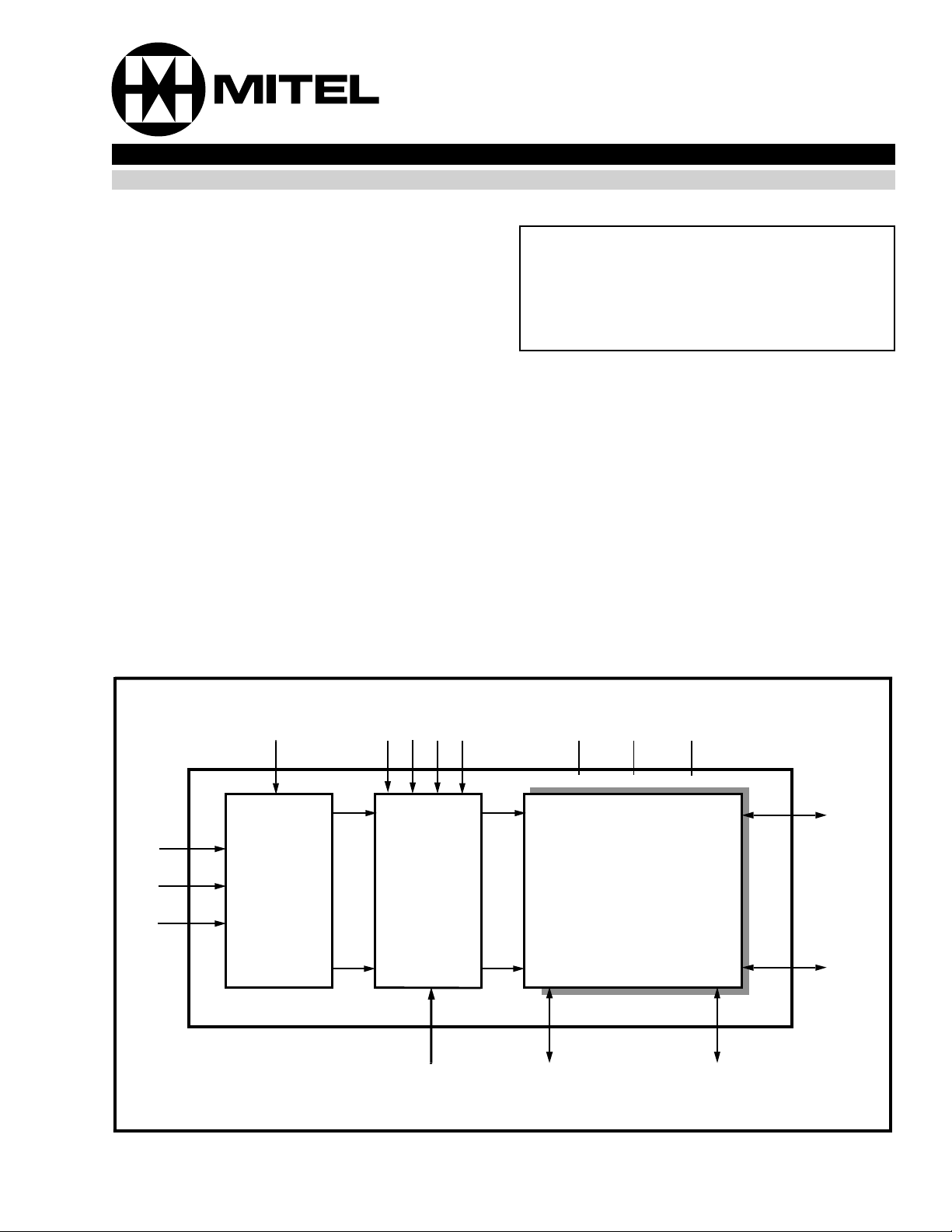
A0
A1
A2
AE D0 D1 D2 D3 VDD VEE VSS
11
3 to 8
Decoder
Latches
832
• • • • • • • • • • • • • • • • • • •
MR Ji I/O (i=0-3)
8 x 4
Switch
Array
Figure 1 - Functional Block Diagram
• • • • • • • • • • • • • • • •
Li I/O
(i=0-7)
3-3
3-3
Page 2
MT8804A CMOS
1
L2
2
L1
3
L0
4
D0
5
J0
D1
6
J1
7
D2
8
J2
9
D3
10
J3
VSS
11
12
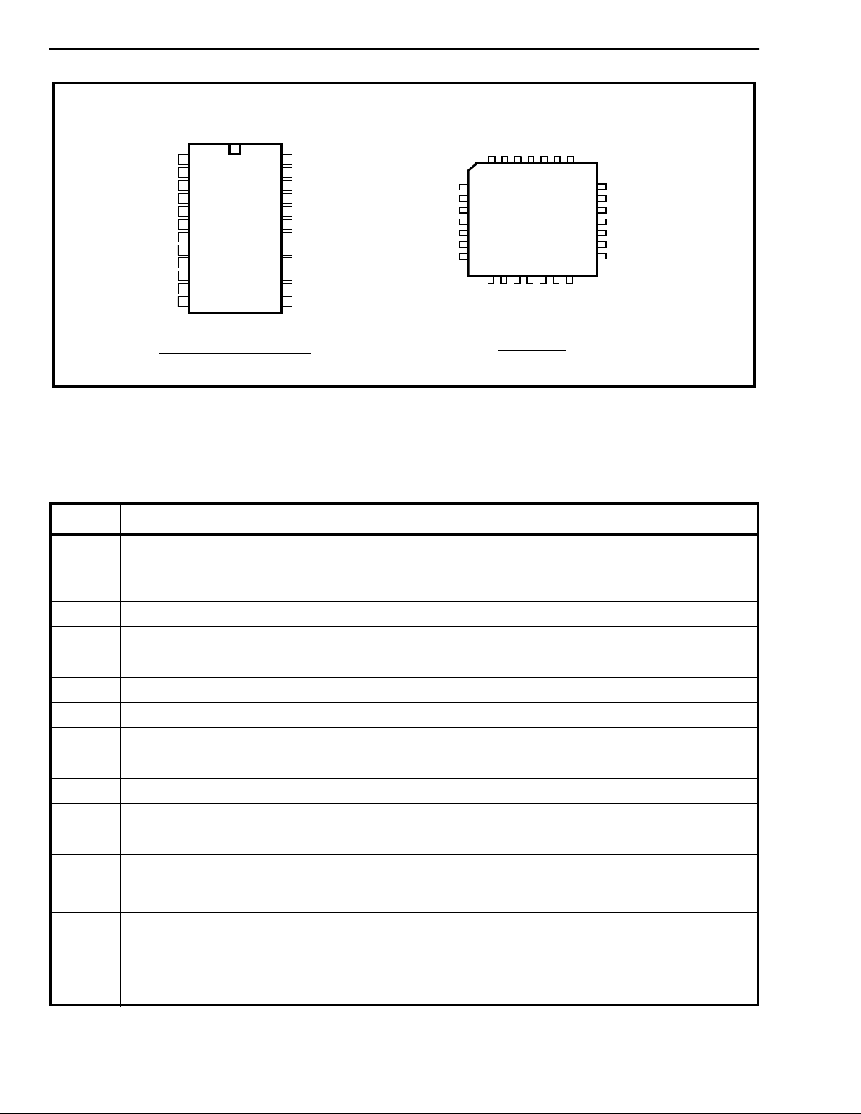
24 PIN CERDIP/PLASTIC DIP
24
23
22
21
20
19
18
17
16
15
14
13
VDD
L3
L4
L5
L6
L7
MR
AE
A2
A1
A0
VEE
NC
D0
J0
D1
J1
D2
J2
Figure 2 - Pin Connections
Pin Description
Pin #* Name Description
C
N
4
5
6
7
8
9
10
11
2
1
3
D
28 PIN PLCC
D
D
1
0
L
3
3
1
3
J
3
4
2
L
L
V
L
L
2
8
7
1
6
2
2
2
•
4
7
6
5
1
1
1
1
0
1
E
S
A
A
E
S
V
V
L5
25
L6
24
23
L7
22
MR
21
AE
20
A2
19
NC
8
1
C
N
1-3 L2-L0 L2-L0 Analog Lines (Inputs/Outputs): these are connected to the L2-L0 columns of the
switch array.
4D0D0 Data (Input): Active High.
5J0J0 Analog Junctor (Input/Output): this is connected to the J0 row of the switch array.
6DIDI Data (Input). Active High.
7J1J1 Analog Junctor (Input/Output): this is connected to the J1 row of the switch array.
8D2D2 Data (Input): Active High.
9J2J2 Analog Junctor (Input/Output): this is connected to the J2 row of the switch array.
10 D3 D3 Data (Input): Active High.
11 J3 J3 Analog Junctor (Input/Output): this is connecte d to the J3 row of the switch array.
12 V
13 V
Digital Ground Reference.
SS
Negative Power Suppl y.
EE
14-16 A0-A2 A0-A2 Addr ess Lines (In pu ts) .
17 AE Add ress En abl e/ Str obe (Inpu t): enables function select ed by address and data. Address
must be stable before AE goes high and D0-D3 must be stabl e on the falling edge of the
AE. Active High.
18 MR Master RESET (Input): this is used to turn off all switches. Active Hig h.
19-23 L7-L3 L7-L3 Analog Lines (Inputs/Outputs): these are connected to the L7-L3 columns of the
switch array.
24 V
Positive P ow er Su pp ly.
DD
* Plastic DIP and CERDIP only
3-4
Page 3
Functional Descripti on
The MT8804A is a CMOS/LSI 8 X 4 Analog Switch
Array incorporating an 8 X 4 analog switch array,
address decoder, control memory, and digital logic
level converter.
The analog switch array is arranged in 8 rows and 4
columns. The row input/outputs are referred to as
Lines (L0-L7) and the column input/outputs as
Junctors (J0-J3). The crosspoint analog switches
interconnect the lines and junctors when turned “ON”
and provide a high degree of isolation when turned
“OFF”. Interchannel crosstalk is minimal despite the
high density of the analog switch array. The control
memory of the MT8804A can be treated as an 8
word by 4 bit random access memory. The 8 words
are selected by the ADDRESS (A0-A2) inputs
through the on chip address decoder. Data is
presented to the memory via the four DATA inputs
(D0-D3). This data is asynchronously written into the
control memory whenever the ADDRESS ENABLE
(AE) input is HIGH. A HIGH level written into a
memory cell turns the corresponding crosspoint
switch “ON” while a LOW level causes the crosspoint
to turn “O F F”.
CMOS MT8804A
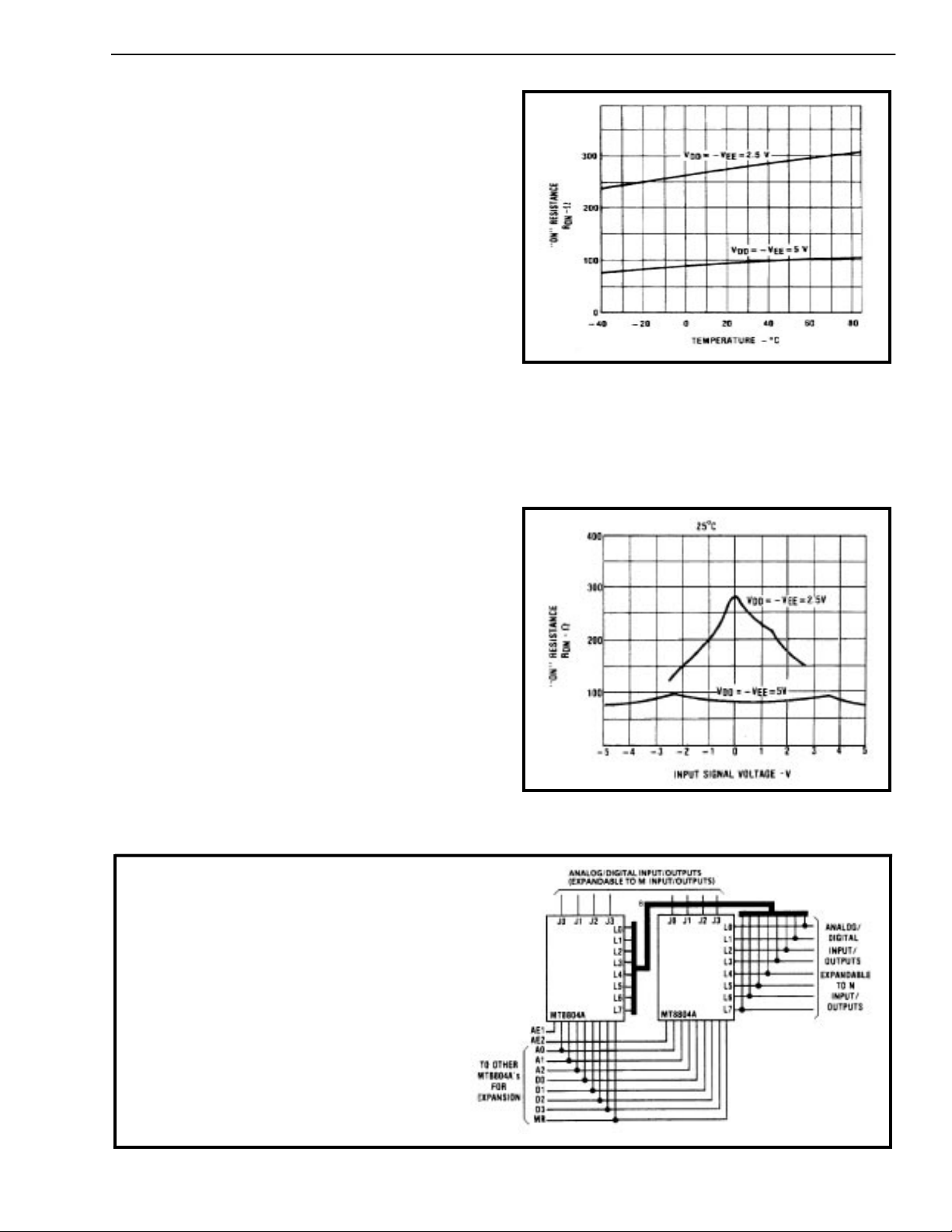
Figure 3 - On Resi stanc e vs. Temperatur e
(Input S ignal Voltage=Supp ly Voltag e/ 2 )
V
=5V, VSS=0V and VEE=-6V, the control inputs
DD
can be driven by a 5V system while the analog
voltages through the crosspoint switches can swing
from +5V to - 6V.
Only the crosspoint switches corresponding to the
addressed memory word are affected when data is
written into the memory. The remaining switches
retain their previous states. By establishing
appropriate patterns in the control memory, any
combination of lines and junctors may be
interconnected. A HIGH level on the MASTER
RESET (MR) input returns all memory locations to a
LOW level and turns all crosspoint switches “OFF”
effectively isolating the lines from the junctors. The
digital logic level converters allow the digital input
levels to differ from limits of the analog levels
switched through the array. For example, with
8x8 Analog/Digital Switch
Two MT8804s configured as shown, implement
an 8 x 8 analog/digital switch. The switch capacity
can be expanded to an M x N array of inputs/
outputs. Expansion in the M dimension is as
shown with the MT8804A lines (L0-L7)
commoned. Expansion in the N dimension is
accomplished by replicating the circuit shown a nd
connecting the MT8804A junctors (J0-J3) in
common. The address and data control inputs of
the MT8804A’s can be connected in common for
any size and switch provided that the address
enable (AE) inputs are driven individually. A
particular signal path is connected by settin g up
the appropriate signals or the address and data
lines and taking the corresponding address
enable input high. The master reset (MR), when
taken high, disconnects all signal paths.
Figure 4 - On Resistance vs. Input Signal Voltage
Figure 5 - 8 x 8 Anal og /Digita l Switch
3-5
Page 4
MT8804A CMOS
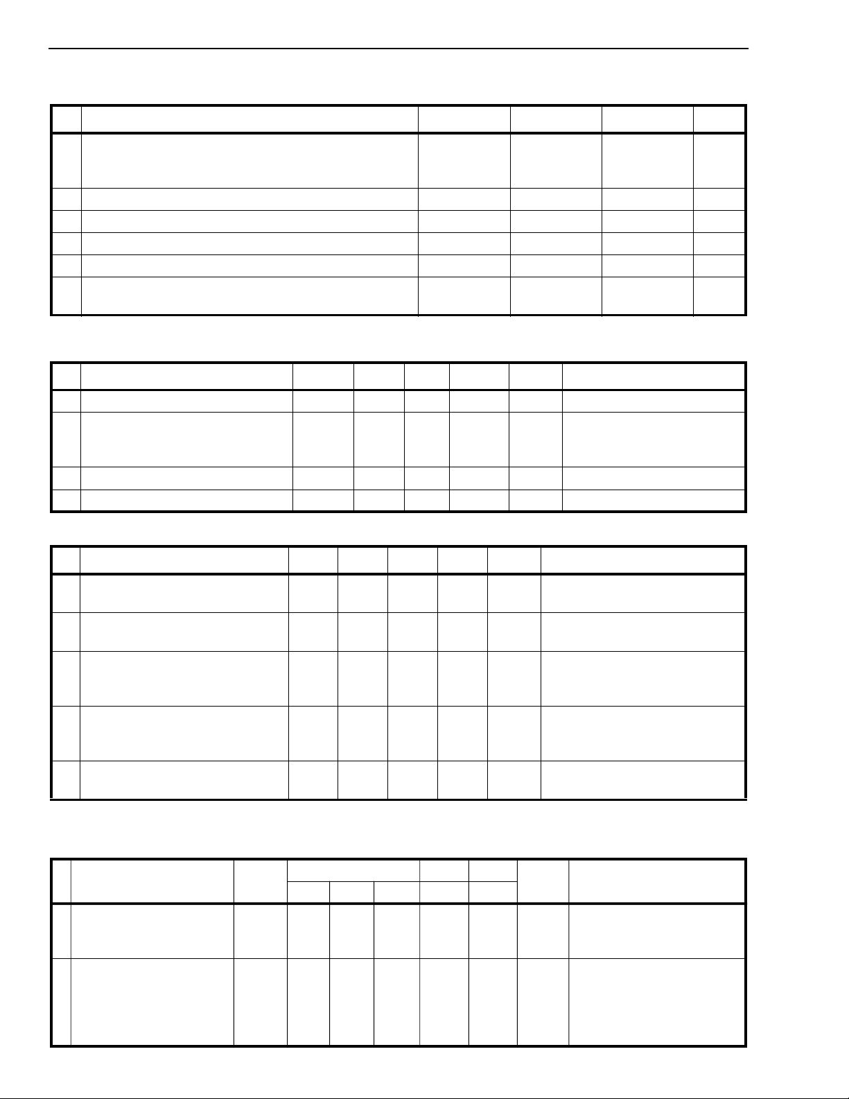
Absolute Maximum Ratings* - Voltages are with respect to V
unless otherwise stated.
EE
Parameter Symbol Min Max Units
1 Su pply Voltage V
DD-VSS
V
DD-VEE
V
SS-VEE
2 An alog In put Voltage V
3 Digit al Input Voltage V
INA
IN
-0.3
-0.3
-0.3
16
16
16
VEE-0.3 VDD+0.3 V
VSS-0.3 VDD+0.3 V
4 Current on any Logic Pin I 10 mA
5 Storage Te mperature T
6 Package Power Dissipation PLASTIC DIP
CERDIP
* Exceeding these values ma y cause perm anen t dama ge. Functi onal operati on und er these cond ition s is not implied.
Recommended Operating Conditions - Voltages are with respect to V
S
P
D
P
D
EE
-65 +150 °C
0.6
1.2
unless otherwise stated.
Characteristics Sym Min Typ Max Units Test Condi tio ns
1 Operat ing Temperat ure
2 Supply Voltage
3 Analog Input Voltage
4 Digit al Inpu t Voltage
T
VDD-V
VDD-V
VSS-V
V
INA
V
O
IN
-40 25 85 °C
SS
EE
EE
5
5
0
V
EE
V
SS
5
10
5
V
V
15
15
10
DD
DD
V
V
V
V
V
V
V
V
W
W
DC Electrical Characteristics
Characteristics Sym Min Typ
1 Quiescent Supply Current I
2 Off-state Leakage Current
†
- Voltages are with respect to V
‡
1100µAVDD=15V. All digital input s at
±0.1 ±500 nA VDD=13V, Swit ch is ‘Off ’
I
OFF
DD
=0V.
EE=VSS
Max Units Test Cond itions
(Any line to any junctor)
3 Input Logic “0” level V
IL
3.0
1.5
4 Input Logic “1” level V
7.0
IH
3.5
5 Maximum curren t thro ugh
I
MAX
±8.0 mA VDD=13V
Crosspoint Switch
† DC Electrical Characteristics are at ambient temperature (25°C).
‡ Typ ical figures are for design aid only; not guaranteed and not subject to product ion testin g.
DC Electrical Characteristics- Switch Resistance - V
is the external DC offset applied at the analog I/O pins.
DC
Characteris tics Sym 25°C 70°C 85°C Units Test Conditions
Min Typ Max Typ Typ
1 On-state V
Resistance V
=13V
DD
=10V
DD
= 5V
V
DD
R
ON
60 90
105
290
108
160
650
105
120
320
110
125
325
2 Difference in on-state
resistance between
two switches
V
=13V
DD
V
=10V
DD
∆R
ON
20
30
20
30
20
30
V
V
V
V
V
IN=VSS
IV
or V
DD
- VLjI = VDD - V
Ji
VDD =10V
V
=5V
DD
V
INA=VDD
through 1kΩ
VDD =10V
V
=5V
DD
V
Ω
Ω
INA=VDD
through 1kΩ
VSS=VEE=0V,VDC=VDD/2,
IV
- VLjI = 0.6V
Ji
Ω
Ω
VSS=VEE=0V,VDC=VDD/2,
Ω
IV
- VLjI = 0.6V
Ji
EE
3-6
Page 5
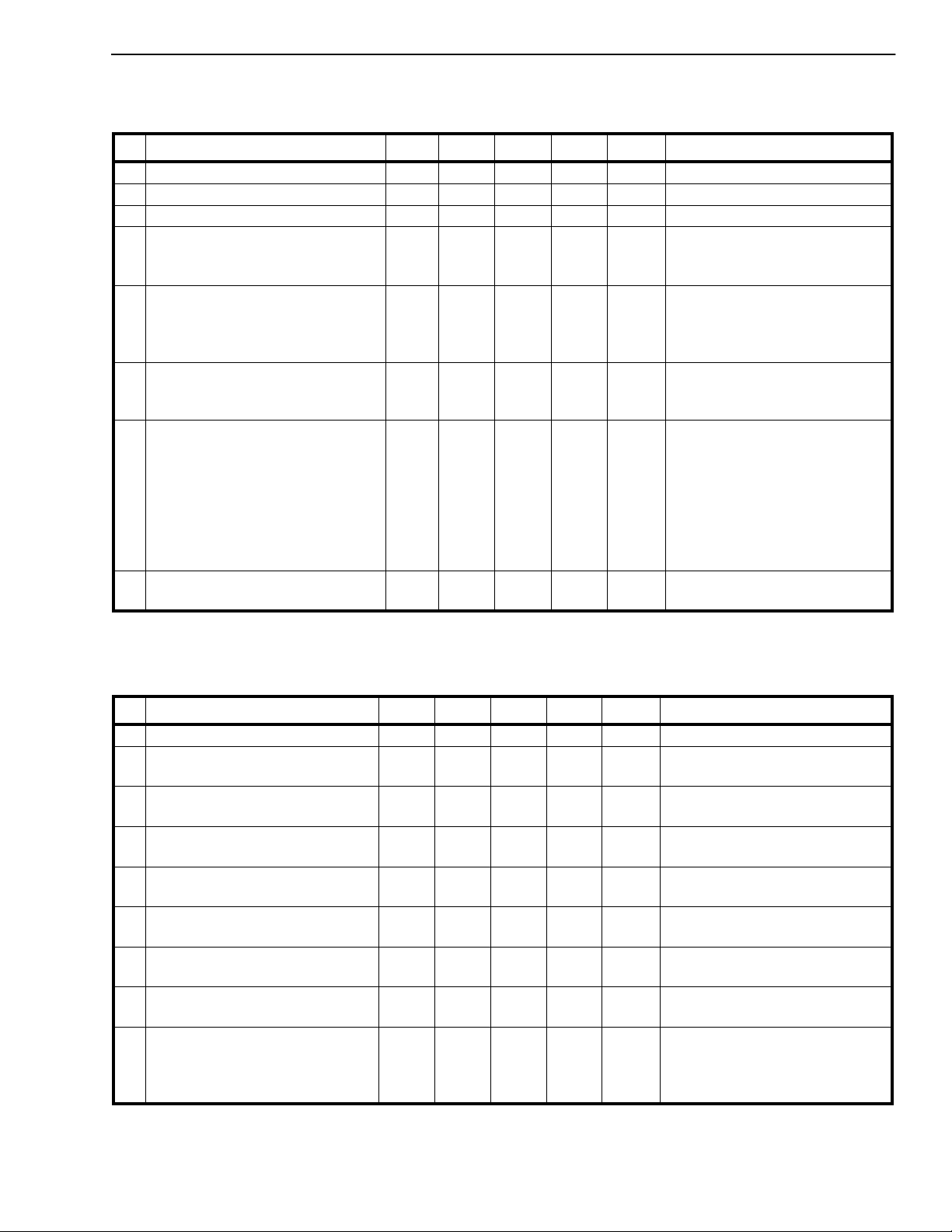
AC Electrical Charac teristic s
I/O pins. Voltages are with respect to V
Characteristics Sym Min Typ
1 Switch Line Capacitance C
2 Switch Junctor Capacitance C
3 Feedthrough Capacit ance C
4 Frequency Response
†
- Crosspoint Performance -V
=10V, VSS=VEE=0V unless otherwise stated.
DD
‡
Max Units Test Conditions
5pF
20 pF
0.2 pF
40 MHz Switch is “ON”; VDC=5V,
F
IS
OS
I
3dB
DC
Channel “ON”
/ V
20LOG(V
OUT
5 Total Harmonic Distortion
=15V/VDC=7.5V
V
DD
V
=10V/VDC=5V
DD
V
=5V/VDC=2.5V
DD
6 Feedthrough
) = -3dB
INA
THD
0.1
0.2
1.0
FDT -50 dB All Switches “OFF”; V
Channel “OFF”
Feed.=20LOG (V
7 Crosstalk between any two
OUT
/ V
INA
)
X
talk
-40
channels for switches Li - Ji and
Lj - Jj.
-90
Li - Ji is “ON“
Lj - Jj is “OFF“
Xtalk=20LOG (V
8 Propagation delay through
Jj/VLi
).
t
PS
10 ns
switch
† AC Electrical Characteristics are at ambient temperature (25°C).
‡ Typ ical figures are for design aid only; not guaranteed and not subject to product ion testin g .
CMOS MT8804A
is the external DC offset applied at the analog
V
=5Vpp sinewave
%
%
%
dBdBV
INA
f= 1kHz; R
Switch is “ON”; V
V
=5Vpp sinewave
INA
f= 1kHz;
R
= 10kΩ
L
5Vpp sinewave f= 1MHz;
R
= 1kΩ. VDC=5V
L
=2Vpp sinewave
INA
f= 1.0MHz; R
V
=2Vpp sinewave
INA
f= 3.4kHz; R
= 5V
V
DC
=50pF
CL
= 1kΩ
L
EE=VSS
= 600Ω.
L
= 600Ω.
L
INA
=0V
=
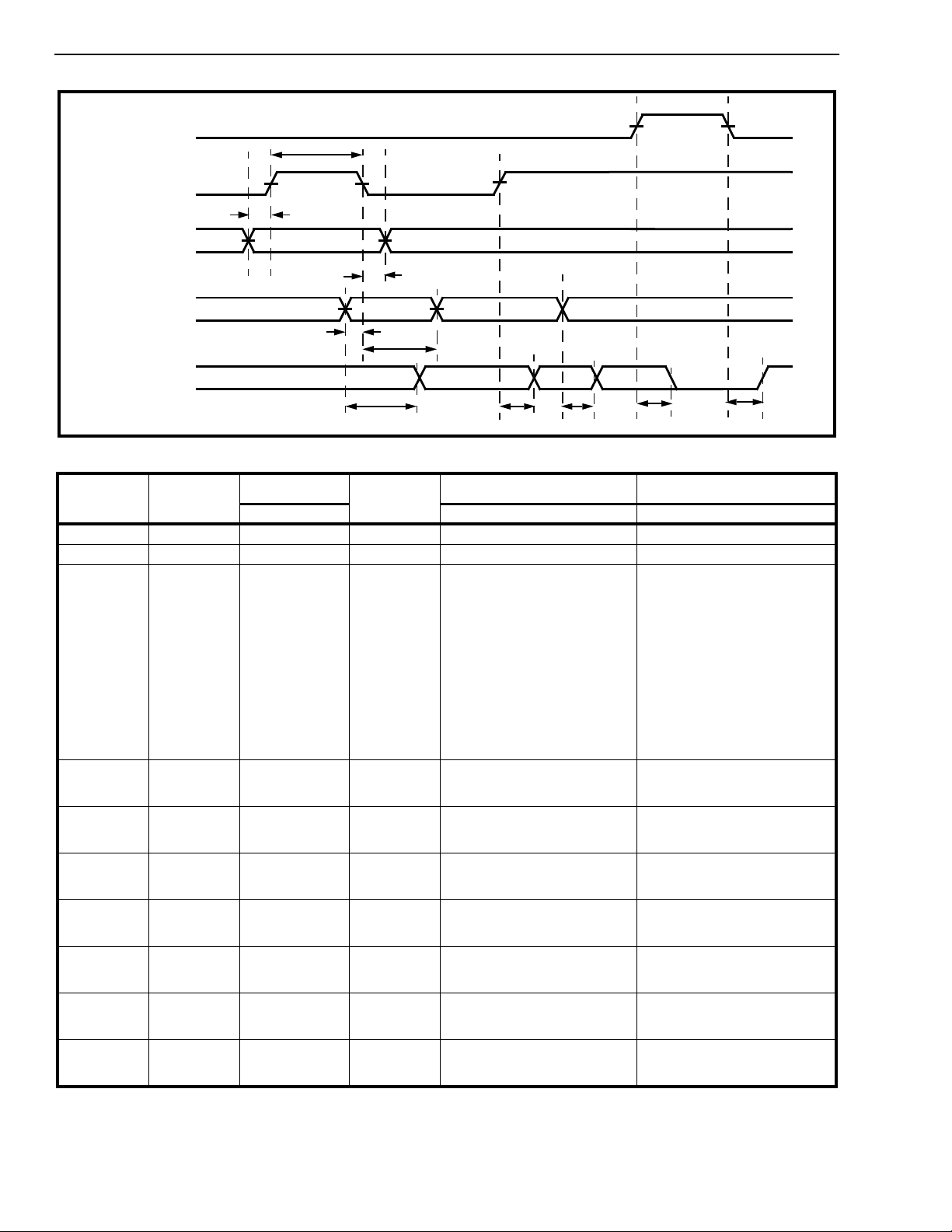
AC Electrical Characteristics† - Control and I/O Timings- Voltages are with respect to V
otherwise stated.
Characteristics Sym M in Typ
1 Digital Input Capacitance C
2 Setup Time D0-D3 to AE t
DS
DI
150
200
3 Hold Time D0-D3 to AE t
DH
120
300
4 Setup Time Address to AE t
AS
0
50
5 Hold Time Address to AE t
AH
120
300
6 AE Pulse Width t
AEW
100
250
7 AE to Switch Status Delay t
8 DATA to Switch Status Delay t
9 MR to Switch Status Delay t
† AC Electrical Characteristics are at ambient temperature (25°C).
‡ Typ ical figures are for design aid only; not guaranteed and not subject to product ion testin g .
Note 1 R
Note 2 RL= 1kΩ, CL=50pF
Digital Inp ut ris e tim e (t r) an d fall time (tf) = 5ns .
= 10kΩ, CL=50pF
L
PAE
PLH
t
PHL
MR
t
MRR
‡
Max Units Test Conditions
5pFV
DD
=10V
nsnsVDD=10V
V
=5V
DD
nsnsVDD=10V
V
=5V
DD
nsnsVDD=10V
V
=5V
DD
nsnsVDD=10V
V
=5V
DD
nsnsVDD=10V
V
=5V
DD
200
650
250
650
250
500
200
500
300
900
400
1000
400
600
350
750
nsnsVDD=10V
V
=5V
DD
nsnsVDD=10V
V
=5V
DD
ns
VDD=10V
ns
V
=5V
ns
ns
DD
V
=10V
DD
V
=5V
DD
=0V unless
SS=VEE
See Note 1
See Note 1
See Note 2
3-7
Page 6
MT8804A CMOS
MR
AE
ADDRESS
D0-D3
SWITCH
ON
OFF
t
AS
50%
t
AEW
50%50%
50%
t
AH
50% 50%
t
DS
t
PLH/tPHL
t
DH
50%
t
PAE
50% 50%
t
PLH/tPHL
t
MR
Figure 6 - Control Memory Timing Diagram
Memory
Reset
MR
Address
Enable
AE
Address
A2 A1 A0 D3 D2 D1 D0 J3 J2 J1 J0
Addressed
Line
Input Data To Control
Memory
1 X X X X ALL X X X X All Switches "OFF"
0 0 X X X NONE X X X X No Change of State
0
0
0
0
0
0
0
0
0
0
0
0
0
0
0
0
0
↓
0
0
↓
0
0
↓
0
0
↓
0
0
↓
0
0
↓
0
0
↓
0
1
1
1
1
1
1
1
1
1
1
1
1
1
1
1
1
1
↓
1
1
↓
1
1
↓
1
1
↓
1
1
↓
1
1
↓
1
1
↓
1
0
0
0
0
0
0
0
0
0
0
0
0
0
0
0
0
0
↓
0
0
↓
0
0
↓
0
1
↓
1
1
↓
1
1
↓
1
1
↓
1
0
0
0
0
0
0
0
0
0
0
0
0
0
0
0
0
0
0
0
0
0
0
0
0
0
0
0
0
0
0
0
1
↓
↓
0
1
1
0
↓
↓
1
0
1
1
↓
↓
1
1
0
0
↓
↓
0
0
0
1
↓
↓
0
1
1
0
↓
↓
1
0
1
1
↓
↓
1
1
0
0
L0
L0
L0
L0
L0
L0
L0
L0
L0
L0
L0
L0
L0
L0
L0
L0
L1
↓
L1
L2
↓
L2
L3
↓
L3
L4
↓
L4
L5
↓
L5
L6
↓
L6
L7
↓
L7
0
0
0
0
0
0
0
0
1
1
1
1
1
1
1
1
0
↓
1
0
↓
1
0
↓
1
0
↓
1
0
↓
1
0
↓
1
0
↓
1
0
0
0
0
1
1
1
1
0
0
0
0
1
1
1
1
0
↓
1
0
↓
1
0
↓
1
0
↓
1
0
↓
1
0
↓
1
0
↓
1
0
0
1
1
0
0
1
1
0
0
1
1
0
0
1
1
0
↓
1
0
↓
1
0
↓
1
0
↓
1
0
↓
1
0
↓
1
0
↓
1
0
1
0
1
0
1
0
1
0
1
0
1
0
1
0
1
0
↓
1
0
↓
1
0
↓
1
0
↓
1
0
↓
1
0
↓
1
0
↓
1
Junctors Connected To
•
•
•
•
•
•
•
•
+
+
+
+
+
+
+
+
•
↓
+
•
↓
+
•
↓
+
•
↓
+
•
↓
+
•
↓
+
•
↓
+
Table 1 - Address Decode Truth Table
NOTES: 0 - Low Logic Level
1 - High Logic Level
X - Don’t Care Condition
+ - Ind ic at es C o nn ec ti on Betwee n Ju nc to r a nd Addres se d Line
• - Ind ic a tes No C o nn ec ti on B e twee n Ju nc to r a nd Ad dr e s se d Li ne
t
MRR
Addressed Line
•
•
•
•
+
+
+
+
•
•
•
•
+
+
+
+
•
↓
+
•
↓
+
•
↓
+
•
↓
+
•
↓
+
•
↓
+
•
↓
+
•
•
+
+
•
•
+
+
•
•
+
+
•
•
+
+
•
↓
+
•
↓
+
•
↓
+
•
↓
+
•
↓
+
•
↓
+
•
↓
+
•
+
•
+
•
+
•
+
•
+
•
+
•
+
•
+
•
↓
+
•
↓
+
•
↓
+
•
↓
+
•
↓
+
•
↓
+
•
↓
+
3-8
 Loading...