

Page 1

E2E1034 -27-Y4
¡ Semiconductor MSM82C43
¡ Semiconductor
This version: Jan. 1998
Previous version: Nov. 1996
MSM82C43
INPUT/OUTPUT PORT EXPANDER
GENERAL DESCRIPTION
The MSM82C43 is an input/output port expander device based on CMOS technology and
designed to operate at low power consumption levels.
In systems employing the MSM80C48/49 8–bit single chip microcomputers, 4–bit data can be
expanded by dividing between four I/O lines by executing the MOVDA, Pp, A and ORLDPp,
A instructions.
FEATURES
• CMOS technology for low power consumption
• 2.5 to 6 V single power supply (dependent on MSM80C48/49 operating frequency.)
• Fully static operation
• Bidirectional I/O ports
• TTL coimpatible (ports 4 thru 7)
• Functional compatiblity with Intel i8243
• Package options
24 pin Plastic DIP (DIP24–P–600-2.54) : (Product name : MSM82C43RS)
24 pin Plastic SOP (SOP24–P–430–1.27-K) : (Product name : MSM82C43GS-K)
1/13
Page 2
¡ Semiconductor MSM82C43
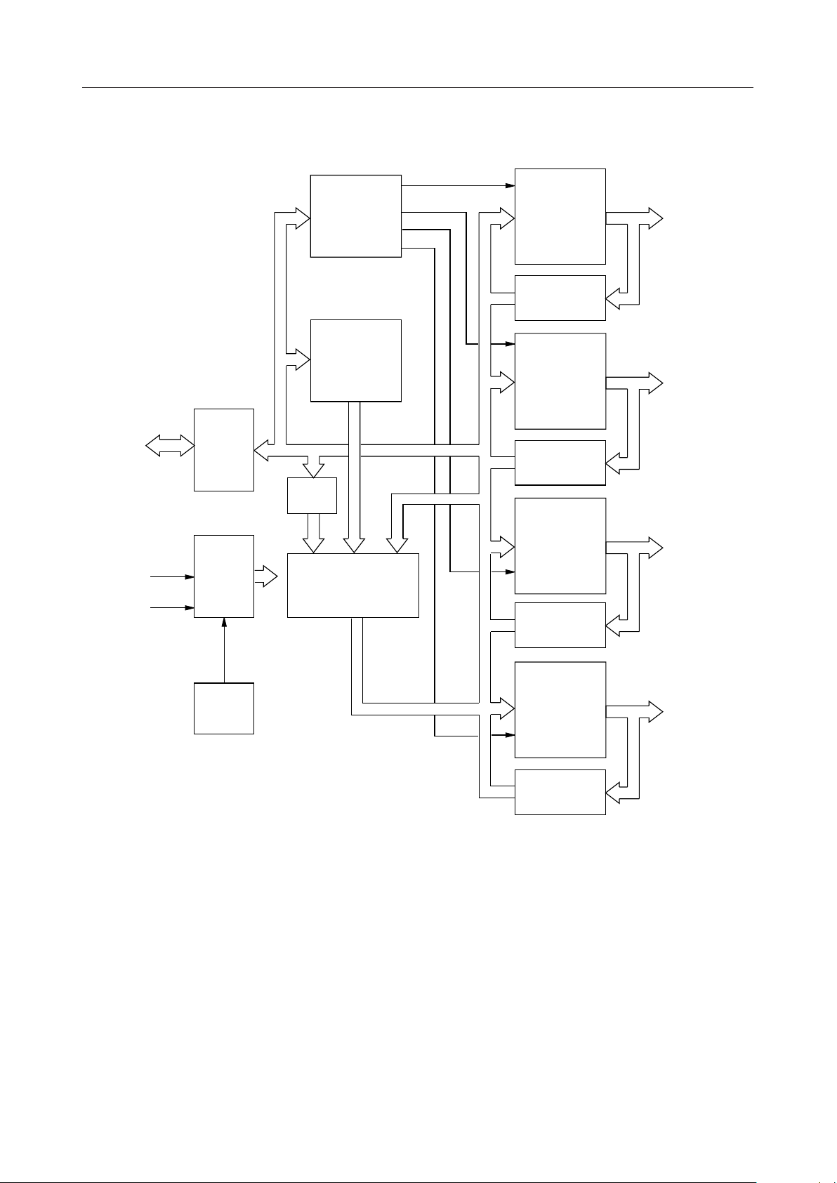
FUNCTIONAL BLOOK DIAGRAM
PORT 2
PROG
CS
4
MUX
CONTROL
ADDRESS
DECODER
INSTRUCTION
DECODER
TEMP
AND/OR
LOGIC
LATCH
PORT 4
4
INPUT
BUFFER
LATCH
PORT 5
4
INPUT
BUFFER
4
LATCH
PORT 6
4
INPUT
4
BUFFER
RESET
CIRCUIT
LATCH
INPUT
BUFFER
PORT 7
4
2/13
Page 3
¡ Semiconductor MSM82C43
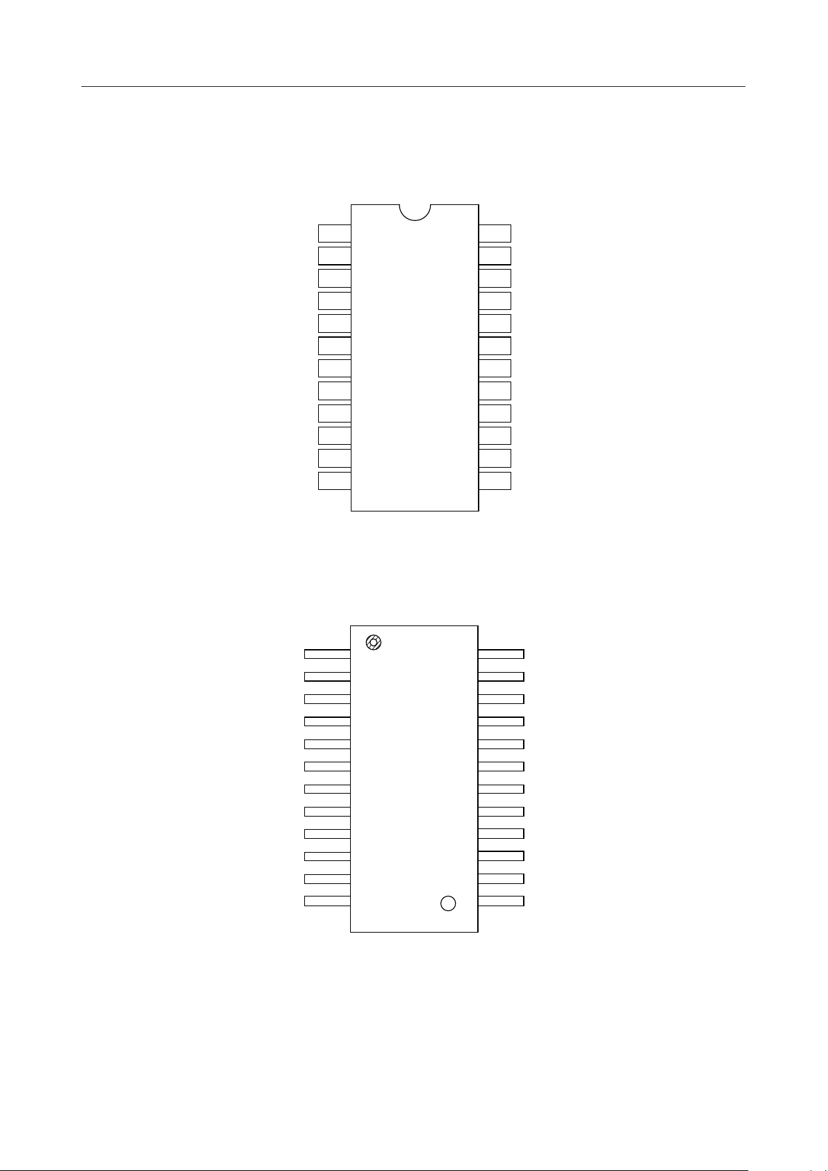
PIN CONFIGURATION (TOP VIEW)
MSM82C43RS
P50
P40
P41
P42
P43
CS
PROG
P23
22
P21
P20
GND
1
2
3
4
5
6
7
8
9
10
11
12
24-pin Plastic DIP
MSM82C43GS
24
23
22
21
20
19
18
17
16
15
14
13
V
CC
P51
P52
P53
P60
P61
P62
P63
P73
P72
P71
P70
P50
P40
P41
P42
P43
CS
PROG
P23
22
P21
P20
GND
1
2
3
4
5
6
7
8
9
10
11
12
24
23
22
21
20
19
18
17
16
15
14
13
24 pin Plastic Small Outline Package
V
CC
P51
P52
P53
P60
P61
P62
P63
P73
P72
P71
P70
3/13
Page 4
¡ Semiconductor MSM82C43
ABSOLUTE MAXIMUM RATINGS
Parameter Symbol Conditions Rating Unit
Supply Voltage
Input Voltage
Storage Temperature
V
CC
V
I
T
STG
Ta=25∞C
Ta=25∞C
—
–0.5 to 7
–0.3 to 7
–65 to +150
V
V
∞C
RECOMMENDED OPERATING CONDITIONS
Parameter Symbol Conditions Range Unit
Supply Voltage
Ambient Temperature
Fan–out
V
CC
T
A
N
—
—
MOS load
2.5 to 6*1
–40 to +85
10
V
∞C
—
TTL load 3*2 —
4/13
Page 5

¡ Semiconductor MSM82C43
ELECTRIC CHARACTERISTICS
DC Characteristics
=4.0V to 6.0V, Ta=–40∞C to +85∞C)
(V
CC
Parameter Symbol Conditions Unit
"L" Input Voltage V
"H" Input Voltage V
"L" Output Voltage Ports 4-7
"L" Output Voltage Ports 7
"L" Output Voltage Ports 2
V
V
V
"L" Total Output Current from
Ports 4-7*3
"H" Output Voltage Ports 4-7
"H" Output Voltage Ports 2
"H" Output Voltage Ports 4-7
"H" Output Voltage Ports 2
V
V
V
V
Input Leak Current*3
Input Leak Current*6
Power Supply Current I
OL1
OL2
OL3
I
OH1
OH2
OH1
OH2
I
IL1
I
IL2
CC
OL
IL
IH
—
—
IOL=5mA
=20mA
I
OL
=0.9mA
I
OL
5mA/1PIN
=–240mA
I
OH
=–100mA
I
OH
=–40mA
I
OH
=–20mA
I
OH
0V
INVCC
0VINV
CC
"Standby stop
No accessing
For continuous
MSM80C49 access-
ing at 11 MH
Z
Min. Typ. Max.
–0.5 — 0.13V
0.4V
—
—
—
—
0.75V
0.75V
0.93V
0.93V
–10
–10
—
—
CC
CC
CC
CC
CC
—V
—
—
—
—
—
—
—
—
—
—
5
1
CC
0.45
1
0.45
80
—
—
—
—
20
10
100
2
V
CC
V
V
V
V
V
V
mA
V
V
V
V
mA
mA
mA
mA
*1 The supply voltage during operation is dependent on MSM80C49 operating frequency.
*2 Except P20 thru P23.
*3 P40 thru P43, P50 thru P53, P60 thru P63, P70 thru P73.
*4 P70 thru P73.
*5 P20 thru P23.
*6 P20 thru P23, CS, PROG.
5/13
Page 6

¡ Semiconductor MSM82C43
AC CHARACTERISTICS
CC
=4.0V to 6.0V, Ta=–40∞C to +85∞C)
(V
Parameter Symbol Conditions Unit
Port Control Setting Time (up to PROG
Falling Edge.)
Port Control Holding Time (up to PROG
Falling Edge.)
Output Data Setting Time
Output Data Holding Time
Input Data Holding Time
PROG Pulse Width
CS Valid Time (before and after PROG)
Output Data Valid Time (at Ports 4-7)
Input Data Holding Time (at Ports 4-7)
Input Data Holding Time (from PROG
Falling Edge)
t
t
t
LP1
t
ACC
t
t
t
t
t
t
CS
PO
A
B
C
D
H
K
80pF LOAD
20pF LOAD
80pF LOAD
20pF LOAD
20pF LOAD
—
—
100pF LOAD
—
80pF LOAD
Min. Max.
50
60
200
20
0
700
50
—
100
—
—
—
—
—
150
—
—
700
—
650
ns
ns
ns
ns
ns
ns
ns
ns
ns
ns
6/13
Page 7

¡ Semiconductor MSM82C43
TIMING CHART
t
PROG
K
P20 thru P23
(When writing)
P20 thru P23
(When reading)
P40 thru P43
|
P70 thru P73
(When writing)
P40 thru P43
|
P70 thru P73
(When reading)
t
A
t
B
t
C
t
D
INSTRUCTION FLOAT DATA FLOAT
t
t
ACC
H
INSTRUCTION OUTPUT DATA
t
PO
OUTPUT DATAPREVIOUS OUTPUT DATA
t
LPI
t
LPI
INPUT VALID
t
CS
t
CS
CS
7/13
Page 8

¡ Semiconductor MSM82C43
PIN FUNCTIONS
Pin
PROG
CS
P20 – P23
P40 – P43
P50 – P53
P60 – P63
P70 – P73
V
CC
GND
Clock input from MSM80C49. When PROG is changed from "H" to "L", MSM82C43 STARTS
operating in accordance with an order from MSM80C49.
Input for chip select. Outputs and internal status cannot be changed when CS is "H".
4-bit bidirectional I/O ports. When connected to P20 thru P23 of MSM80C49, direct data
transfer from port to accumulator and from accumulator to port is possible.
4-bit bidirectional I/O ports.
Data is latched statistically when output to ports, but is only valid while PROG is at "L" level
when input.
+5V power supply
GROUND
Function
FUNCTIONS
Power-on reset mode
Upon powered on, ports to 7 are 3-stated, and 2 is put into an input mode.
Write mode
Execution of MOVDPp, A, ORLDPp, A, ANLDPp, and A by MSM80C49 enables direct output
of accumulator contents to ports 4 thru 7, and output to the ports after ORing or ANDing with
port data. The port data is latched statistically at this time and remains unchanged until
execution of the next instruction.
Read mode
Execution of MOVDA andPp results in data of ports 4 thru 7 being accepted by the accmulator.
Note that port data is valid only while PROG is at "L" level. When at "H" level, ports 4 thru 7 are
switched to tristate and port 2 is switched to input mode.
Address and instruction code
Instruction PortP23 P22 P21 P20
Read Port 400 00
Write Port 501 01
OR Port 610 10
AND Port 711 11
8/13
Page 9

¡ Semiconductor MSM82C43
MSM82C43 Multiple connection example
PORT
MSM80C49
PROG
P20
–P23
SELECTOR
CS
PROG
P20
–P23
CS
PROG
P20
–P23
CS
PROG
P20
–P23
9/13
Page 10

¡ Semiconductor MSM82C43
p
)
OUTPUT CHARACTERISTICS
Standard dc characteristics
Output "H" voltage (VOH) vs. output currnt (IOH)
tPO, tH, and t
vs. power supply voltage (VCC)
ACC
Ta=25°C
5
(V)
4
OH
3
2
1
Output "H" voltage V
0 –1–2–3–4–5
Output current I
OH
(mA)
Output "L" voltage (VOH) vs. output currnt (IOH)
Ta=25°C
5
4
(V)
OL
3
700
600
500
(ns)
H
, t
400
ACC
, t
300
PO
t
200
100
0
3
Power supply voltage (V
Ta=25°C
t
ACC
t
PO
t
H
56
)
CC
2
1
Output "L" voltage V
0 –1–2–3–4–5
Output current I
OL
(mA)
Operating frequency vs. power supply voltage (ICC)
Ta=25°C
2
(mA)
CC
1
Power supply current I
0
136 11
MSM80C49 o
erating frequency (MHz
Note: The direction which the output current flows through the device is taken as the positive
direction.
10/13
Page 11

¡ Semiconductor MSM82C43
GUARANTEED MSM82C43 OPERATING RANGE
Ta=–40 to +85°C
Guaranteed operating range
3
MSM80C49 operating range (MHz)
6
11
23456
Power supply voltage (VCC)
11/13
Page 12

¡ Semiconductor MSM82C43
PACKAGE DIMENSIONS
(Unit : mm)
DIP24-C-600-2.54
24 13
15.11±0.25
0.25
12
15.24
5.10MAX
2.80±0.40
SEATING PLANE
0.51MIN
M
2.54MIN
+0.15
0.25-0.05
1
INDEX MARK
1.27TYP
1.27TYP
2.54
30.8MAX
0.50±0.10
Notes for Mounting the Surface Mount Type Package
The SOP, QFP, TSOP, SOJ, QFJ (PLCC), SHP and BGA are surface mount type packages, which
are very susceptible to heat in reflow mounting and humidity absorbed in storage.
Therefore, before you perform reflow mounting, contact Oki’s responsible sales person for the
product name, package name, pin number, package code and desired mounting conditions
(reflow method, temperature and times).
12/13
Page 13

¡ Semiconductor MSM82C43
(Unit : mm)
SOP24-P-430-1.27-K
Mirror finish
Package material
Lead frame material
Pin treatment
Solder plate thickness
Package weight (g)
Epoxy resin
42 alloy
Solder plating
5 mm or more
0.58 TYP.
Notes for Mounting the Surface Mount Type Package
The SOP, QFP, TSOP, SOJ, QFJ (PLCC), SHP and BGA are surface mount type packages, which
are very susceptible to heat in reflow mounting and humidity absorbed in storage.
Therefore, before you perform reflow mounting, contact Oki’s responsible sales person for the
product name, package name, pin number, package code and desired mounting conditions
(reflow method, temperature and times).
13/13
 Loading...