

Page 1

E2D0037-27-41
¡ Semiconductor
¡ Semiconductor
•
Previous version: May. 1997
This version: Jan. 1998
MSM6685
MSM6685
8,388,608-Word x 1-Bit Serial Register
GENERAL DESCRIPTION
The MSM6685 is a serial register composed of 8,388,608 words x one bit, characterized by mediumspeed, low power consumption operation.
This device has a built-in internal address generation circuit allowing continuous serial read/write
operation by external clock input. Read/write operation causes the internal address to be incremented
automatically by +1.
External address input enables addressing in units of 1024 words. Furthermore, a refresh timer and
a refresh address counter are installed, which makes an external refresh circuit unnecessary. In
addition, this configuration allows lower power consumption.
The device is packaged in 26-pin SOJ having a width of 300 mil.
It is well adapted for storing much data by means of a battery backup. Its combination with OKI's
recording and playback IC enables the easy implementation of a solid recording and playback
system.
FEATURES
• Configuration : 8,388,608 ¥ 1 bit
• Serial access operation
Serial access time : 1.5 ms
Serial read/write time : 2.5 ms
• Low current drain : 200 mA max. (VCC = 4 V, at refresh operation, with
data stored and under standard conditions)
• Refresh operation
A self-refresh function is supported.
• Wide range of operating voltage : Single 3.5 to 5.5 V supply
• Addressing : In units of 1024 words
• Process : 0.5 mm double well CMOS process
• Package:
26/20-pin plastic SOJ (SOJ26/20-P-300-1.27) (Product name : MSM6685JS)
1/9
Page 2
¡ Semiconductor
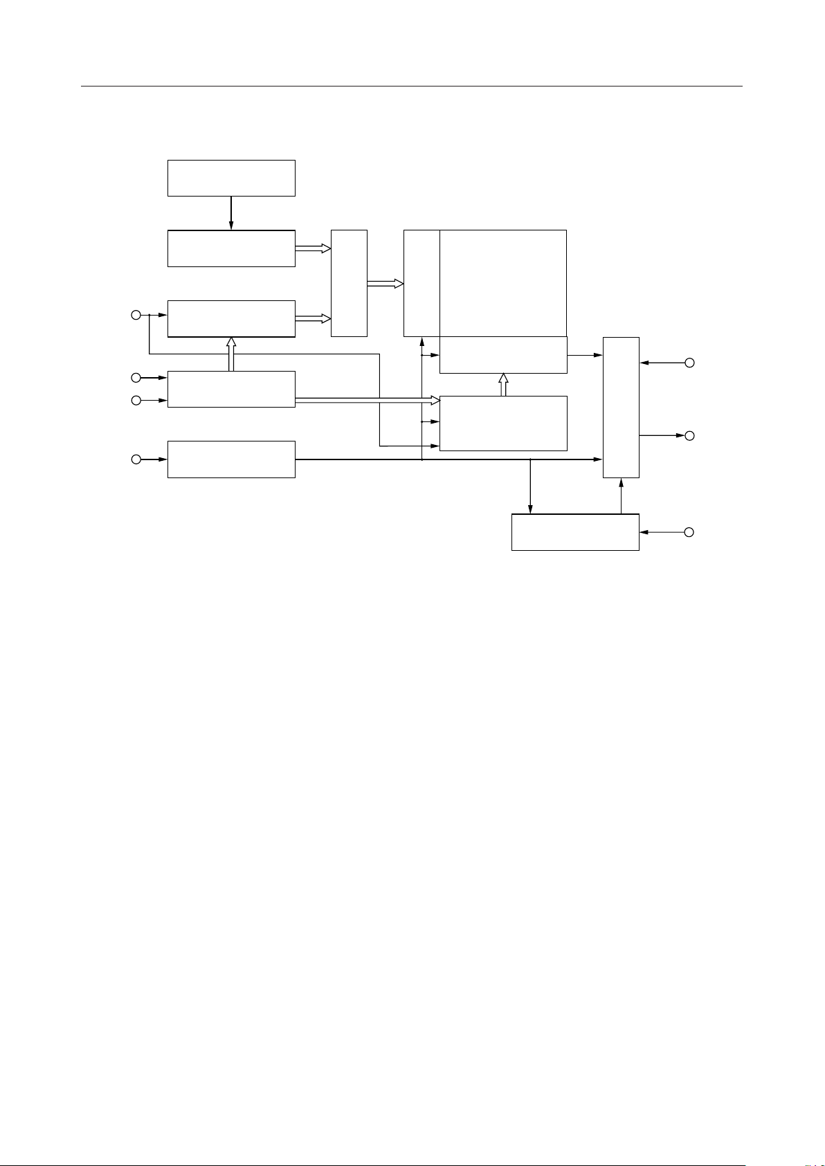
BLOCK DIAGRAM
Refresh Timer
Refresh Address
Counter
TAS
Row Address
Counter
Address
Multiplexer
MSM6685
8,388,608
Data Register
Row Decoder
SAD
SAS
RWSK
Row Address
Register
Timing
Generator
Column Decoder
Column Address
Counter
Write Clock
Generator
I/O Control
DIN
DOUT
WE
2/9
Page 3
¡ Semiconductor
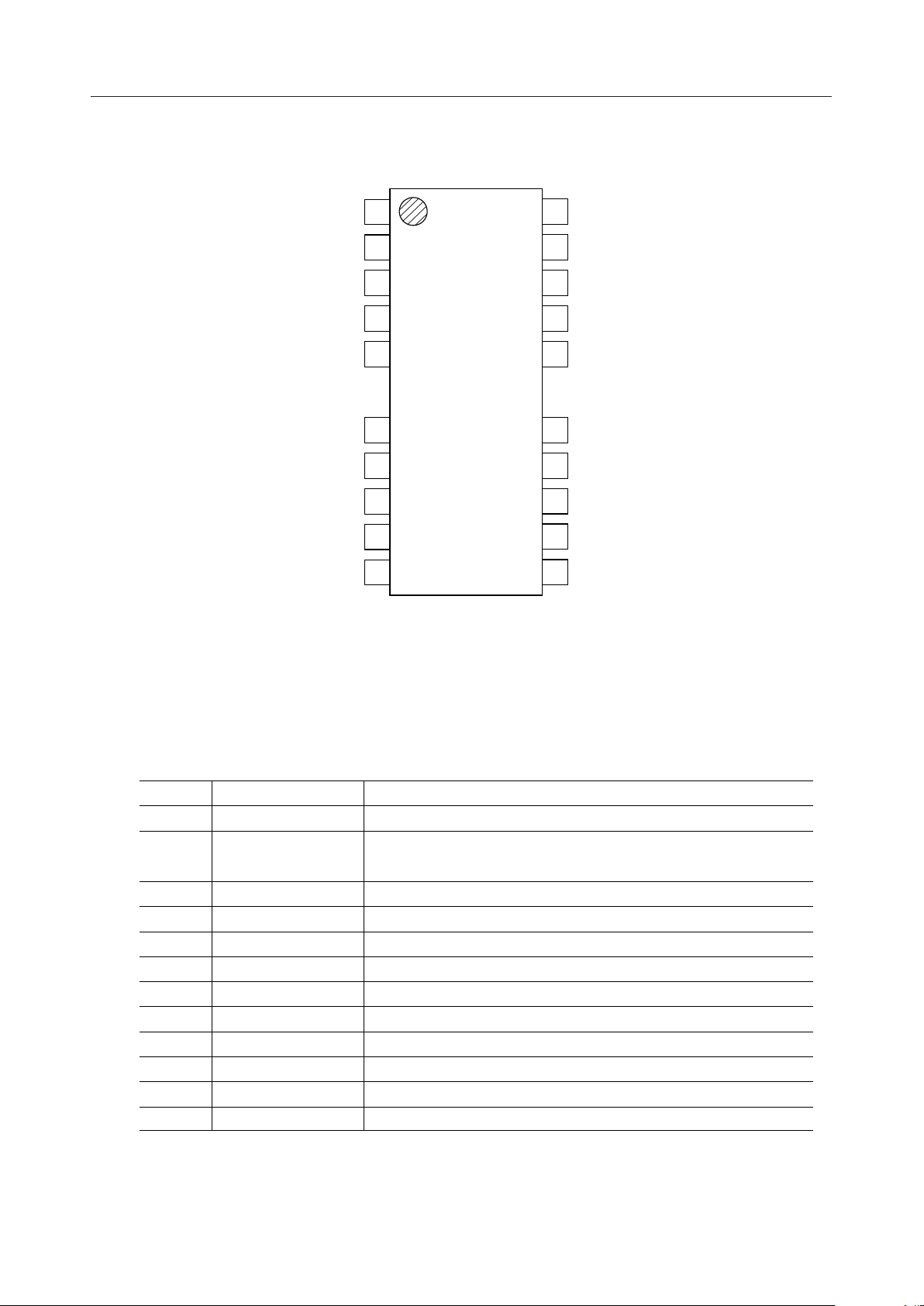
PIN CONFIGURATION (TOP VIEW)
MSM6685
TEST
RWCK
NC
TEST
TEST
TEST
TEST
DIN
NC
V
SS
1
2
3
4
5
9
10
11
12
13
NC : No connection
26
25
24
23
22
18
17
16
15
14
V
CC
TEST
TEST
SAD
SAS
TAS
CS
WE
DOUT
NC
PIN DESCRIPTION
Pin
25
1, 4, 5
9, 10, 24
Symbol
TEST
TEST
RWCK
DIN
V
SS
DOUT
WE
CS
TAS
SAS
SAD
V
CC
26/20-Pin Plastic SOJ
Description
Test input
Test input
Read/write clock2
Data input11
Ground (0 V)13
Data output15
Write enable16
Chip select17
Transfer address strobe18
Serial address strobe22
Serial address data23
Power supply (5 V)26
Note : All TEST pins are to be connected to the power supply.
The TEST pin is to be referenced to the ground level.
3/9
Page 4

¡ Semiconductor
MSM6685
ABSOLUTE MAXIMUM RATINGS
Parameter Symbol Condition Rating Unit
Pin Voltage V
Short-circuit Output Current Ta = 25 °C 50 mA
Power Dissipation 1 W
Operating Temperature — 0 to 70 °C
Storage Temperature — –55 to +150 °C
T
I
P
T
STG
T
OS
D
op
Against VSS at Ta = 25 °C –1.0 to +7.0 V
Ta = 25 °C
RECOMMENDED OPERATING CONDITIONS
(Ta=0 to 70°C)
Parameter Symbol Min Typ Max Unit
Supply Voltage V
Supply Voltage 0 0 0
"H" Input Voltage V
"L" Input Voltage –0.2 0 +0.5
CC
V
SS
V
IH
V
IL
3.5 4.5 5.5
– 0.5 V
CC
CC
V
CC
+ 0.2
V
V
V
V
ELECTRICAL CHARACTERISTICS
DC Characteristics
Parameter Symbol Condition Min Max Unit
"H" Output Voltage V
"L" Output Voltage I
Input Leakage Current I
Output Leakage Current V
Supply Current (Operation) V
Supply Current (Standby) V
V
I
I
CC1
I
CC2
OH
OL
IL
OL
CC
(V
=3.5V to 5.5V, Ta=0 to 70°C)
CC
IOH=–0.5 mA VCC – 0.5 — V
=0.5 mA — 0.4 V
OL
VI=0 V to V
=0 V to V
O
=4 V, t
CC
CC
=1 ms — 20 mA
RWC
=4 V — 200
CC
–1 +1
–1 +1
m
A
m
A
m
A
4/9
Page 5

¡ Semiconductor
MSM6685
AC Characteristics
Parameter Symbol Min Max Unit
Read/Write Cycle Time t
Access Time t
Output Turn-off Delay Time t
I/O Signal Rise Time t
RWCK Pre-charge Time t
RWCK Pulse Time
SAS Cycle Time
SAS Pre-charge Time
SAS Pulse Duration
Address Setup Time
Adress Hold Time
TAS Setup Time
TAS . RWCK Setup Time
TAS Pulse Duration
Read Instruction Setup Time
Read Instruction Hold Time
Write Instruction Setup Time
Write Instruction Hold Time
Write Instruction Pulse Duration
WE. RWCK Read Time
Data Setup Time
Data Hold Time
RWCK. WE Delay Time
RWC
ACC
RWP
t
t
SSC
t
SAP
t
SAS
t
t
t
ATS
t
TRS
t
TAS
t
RRS
t
RRH
t
WRS
t
WRH
t
t
RWL
t
t
t
RWD
OFF
RW
AS
AH
WP
DS
DH
(V
=3.5 V to 5.5 V, Ta=0 to 70°C)
CC
2,500 — ns
— 1,500 ns
050ns
T
350ns
1,000 — ns
1,500 10,000 ns
100 — ns
50 — ns
50 — ns
0—ns
50 — ns
50 — ns
50 — ns
50 — ns
0—ns
250 — ns
0—ns
50 — ns
50 — ns
50 — ns
0—ns
50 — ns
50 — ns
5/9
Page 6

¡ Semiconductor
TIMING DIAGRAM
Read/Write and Read/Modify/Write Cycles
WRH
t
WRS
t
MSM6685
DH
t
DS
t
RWC
t
RWP
t
RW
t
TRS
t
TAS
t
ATS
t
RWL
t
WP
t
RWD
t
RRH
t
RRS
t
DH
t
n+1 n+2
DS
t
OFF
t
n n+1
ACC
t
CS
SSC
t
RWCK
SAP
t
SAS
t
SAS
AH
t
t
A0 A1 A12
AS
SAD
TAS
WE
DIN
DOUT
6/9
Page 7

¡ Semiconductor
MSM6685
PIN FUNCTIONS AND OPERATING MODES
• Serial address input (SAD)
Pin used to enter start address for reading/writing. An address can be specified in units of 1024
words. 1024 words of address data can be entered through the pin as 13 bits (A0 to A12) of serial data.
• Serial address strobe (SAS)
This is a clock pin for latching serial address data into an internal register.
• Address transfer strobe (TAS)
This is an input pin for loading the internal address counter with serial address data latched in the
address register.
• Read/write clock (RWCK)
This is a clock input pin for reading and writing information in the data register. The trailing edge
of RWCK triggers off internal operation. In the reading mode, information in the data register is
output to the DOUT pin. In the writing mode, the data register is loaded with DIN information. A
the leading edge of RWCK, the internal address counter is incremented automatically by +1.
• Write enable (WE)
This is an input pin for selecting the read mode, the write mode, or the read-modify-write mode.
When WE is "H", the read mode is set up and, when WE is "L", the write mode is set up. When the
level is lowered from "H" to "L" with RWCK active, the read-modify-write mode is set up.
• Data input (DIN)
This is a pin for entering write data. Information on the data input pin is latched when the trailing
edge of RWCK is encountered in the write mode and that of WE is encountered in the read-modify
mode.
• Data output (DOUT)
The data output pin always provides high impedance as long as RWCK or CS is kept at "H". When
"H" or "L" information is read, the output pin set at "H" or "L", and information read is held until
RWCK returns to "H" . In the early write mode, the output pin is maintained at high impedance,
so that, connection of DIN and DOUT enables "I/O common operation".
• Chip select (CS)
This is an input pin for disabling all input pins. This pin allows the use of two or more MSM6684A
devices with data input and output pins connected in parallel.
• Test (TEST, TEST)
The TEST pin must always be fixed at "L" and the TEST pin at "H".
7/9
Page 8

¡ Semiconductor
MSM6685
NOTES ON ENERGIZATION
MSM6685 has built-in bias generator and internal power supply circuits, thus, power up must be
followed by a pause of 1 ms or more for internal circuit stabilization. Furthermore, the TEST pin must
be brought "L" concurrently with or prior to VCC, and all clock input pins and TEST pins must be
brought "H" concurrently with or prior to VCC.
To achieve proper operation of internal circuits, the initial pause above must be followed by a
minimum ten dummy read cycles with RWCK for internal circuit initialization.
NOTES ON SUPPLY VOLTAGE VARIATION
When using MSM6685, take precautions so that the supply voltage does not vary over one volt within
a period of 1,000ms or less in the active state.
8/9
Page 9

¡ Semiconductor
PACKAGE DIMENSIONS
SOJ26/20-P-300-1.27
Mirror finish
MSM6685
(Unit : mm)
Package material
Lead frame material
Pin treatment
Solder plate thickness
Package weight (g)
Epoxy resin
42 alloy
Solder plating
5 mm or more
0.80 TYP.
Notes for Mounting the Surface Mount Type Package
The SOP, QFP, TSOP, SOJ, QFJ (PLCC), SHP and BGA are surface mount type packages, which
are very susceptible to heat in reflow mounting and humidity absorbed in storage.
Therefore, before you perform reflow mounting, contact Oki’s responsible sales person for the
product name, package name, pin number, package code and desired mounting conditions
(reflow method, temperature and times).
9/9
 Loading...