

Page 1

E2B0025-27-Y2
¡ Semiconductor MSM6669
¡ Semiconductor
This version: Nov. 1997
Previous version: Mar. 1996
MSM6669
80-DOT LCD SEGMENT DRIVER
GENERAL DESCRIPTION
The MSM6669 is a dot matrix LCD segment driver which is fabricated using CMOS low power
silicon gate technology.
This LSI consists of 80-bit latches I and II, 80-bit level shifter, and 80-bit 4-level driver.
It latches the 4-bit parallel display data from the LCD controller LSI or microcontroller, and then
outputs the signal for the LCD driving.
FEATURES
• Logic supply voltage : 2.7V to 5.5V
• LCD driving voltage : 14V to 28V
• Applicable LCD duty : 1/64 to 1/256
• Bias voltage can be supplied externally
• LCD output : 80
• 4-bit parallel data processing has improved the transfer speed to 1/4 that of the conventional
serial transfer, thereby achieving low power consumption
• Applicable common driver : MSM6778 (120 outputs)
• Structure:
TCP mounting with 35mm wide film (Product name: MSM6669AV-Z-05)
Sn-plated
Outer lead pitch : 220mm
User area : 7.5mm
1/9
Page 2
¡ Semiconductor MSM6669
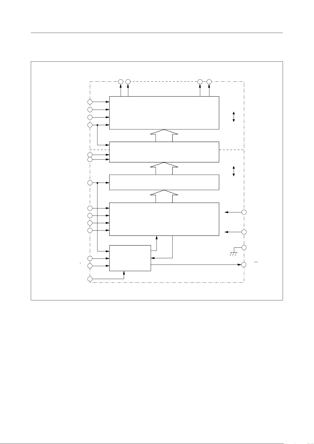
BLOCK DIAGRAM
V
V
V
V
EE
DF
DISP OFF
LOAD
D
D
D
D
O1O
2
1
3
4
80-BIT 4-LEVEL DRIVER
O79O
80
V
DD
V
EE
80-BIT LEVEL SHIFTER
V
DD
V
80-BIT LATCH (II)
0
1
2
3
80-BIT LATCH (I)
SS
V
DD
V
DD
CP
E
SHL
V
SS
CONTROL
I
CIRCUIT
E
O
2/9
Page 3
¡ Semiconductor MSM6669
PIN CONFIGURATION (TOP VIEW)
Dummy
Dummy
Dummy
O
80
O
79
O
78
O
3
O
2
O
1
Dummy
Dummy
Dummy
V
1
V
3
V
4
V
EE
V
SS
SHL
V
DD
E
O
DISP OFF
DF
LOAD
CP
D
3
D
2
D
1
D
0
E
I
V
DD
3/9
Page 4

¡ Semiconductor MSM6669
ABSOLUTE MAXIMUM RATINGS
Parameter UnitCondition
Supply Voltage (1)
Supply Voltage (2)
Input Voltage
Storage Temperature
*V1 > V3 > V4 > VEE, V
Symbol
V
DD
V
LCD
V
I
T
STG
≥ V
DD
1
> V
Ta=25°C –0.3 to +6.5
Ta=25°C, V
– VEE*
DD
Ta=25°C
—
≥ V
3
DD
–10V, V
RECOMMENDED OPERATING CONDITIONS
Parameter UnitCondition
Supply Voltage (1)
Supply Voltage (2)
Operating Temperature
*V1 > V3 > V4 > VEE, V
Symbol
V
DD
V
LCD
T
op
≥ V
DD
1
> V
V
DD–VEE
≥ V
3
—
—
DD
*
–7V, V
+10V ≥ V
EE
Min.
2.7
14
–20
+7V ≥ V
EE
Rating
0 to 30
–0.3 to V
DD
+ 0.3
–30 to +85
> V
4
EE
Typ. Max.
5.0
4
—
—
> V
5.5
28
75
EE
V
V
V
°C
V
V
°C
4/9
Page 5

¡ Semiconductor MSM6669
ELECTRICAL CHARACTERISTICS
DC Characteristics
(VDD = 2.7 to 5.5V, Ta = –20 to +75°C)
Parameter UnitCondition
"H" Input Voltage
"L" Input Voltage
"H" Input Current
"L" Input Current
"H" Output Voltage
"L" Output Voltage
On Resistance
Stand-by Current
Supply Current (1)
Supply Current (2)
Input Capacitance
Symbol
V
IH
V
IL
I
IH
I
IL
V
OH
V
OL
R
ON
I
DDSBY
I
DD1
I
V
C
I
*1
*1
V
*1
*1
*2
*2
*4
= V
IH
DD
VIL = 0V
= –0.2mA
I
O
I
= 0.2mA
O
VDD – VEE = 25V
V
= 2.7V
DD
– VO = 0.25V
V
N
f
= 6.0MHz, VDD = 3.0V
CP
– VEE = 25V
V
DD
No load, f
fCP = 6.0MHz, VDD = 3.0V
V
No load, f
f
CP
V
No load, f
LOAD
– VEE = 25V
DD
LOAD
= 6.0MHz, VDD = 3.0V
– VEE = 25V
DD
LOAD
f = 1MHz
—
—
= 21.6kHz
= 21.6kHz
= 21.6kHz
*3
*5
*6
*7
Typ.Min.
DD
—
—
—
—
—
—
0.8 V
—
V
SS
—
VDD – 0.4
—
—
——
——
——
—
5
Max.
V
DD
0.2 V
1
–1
—
0.4
3.01.5
0.3
1.5 (V
1.0 (V
100
—
DD
DD
V
V
µA
µA
V
V
kΩ
mA
)
mA
)
EE
µA
pF
*1 Applicable to LOAD, CP, D0 to D3,
, DF, DISP OFF pins.
E
I
*2 Applicable to EO pin.
*3 VN = V1 to VEE, V4 = 14/16 (VDD – VEE), V3 = 2/16 (VDD – VEE), VDD = V1.
*4 Applicable to O1 to O80 pins.
*5 Display data 1010, fDF = 45Hz, current that flows from VDD to Vss when the display
data is not clocked in.
*6 Display data 1010, fDF = 45Hz, current (VDD) that flows from VDD to VSS and VEE, and
current (VEE) that flows from VDD to VEE when the display data is clocked in.
*7 Display data 1010, fDF = 45Hz, current that flows to each of the V1, V3 and V4 pins.
5/9
Page 6

¡ Semiconductor MSM6669
Switching Characteristics
= 2.7 to 5.5V, Ta = –20 to +75°C, CL = 15pF)
(V
DD
Parameter UnitCondition
Symbol
Typ.Min.
Max.
Clock Frequency
Clock Pulse Width
Rise/Fall Time
Data Setup Time
Data Hold Time
Load Pulse Width
Load Setup Time
Load → Clock Time
"H", "L" Propagation
Delay Time
E
Setup Time
I
0.8 V
CP
DD
f
CP
t
W1
t
, t
r
t
DSU
t
DHD
t
W2
t
LSU
t
LC
t
PLH
t
PHL
t
ESU
t
W1
0.8 V
f
DD
t
DSUtDHD
Duty = 50%
—
—
—
—
—
—
—
—
—
t
f
0.2 V
DD
t
W1
t
r
0.8 V
0.2 V
DD
—
56
—
50
50
70
80
80
——
50
t
W1
DD
—
—
—
—
—
—
—
—
—
0.8 V
6.5
—
20
—
—
—
—
—
236
—
DD
MHz
ns
ns
ns
ns
ns
ns
ns
ns
ns
D
- D
0
LOAD
CP
LOAD
E
O
0.8 V
3
0.2 V
1 2 18 19 20
t
PLH
0.2 V
0.8 V
DD
DD
DD
t
LSU
t
0.2 V
t
f
0.2 V
0.2 V
t
DD
PHL
DD
LC
DD
t
ESU
0.8 V
DD
t
W2
0.8 V
DD
DD
t
r
E
I
0.2 V
DD
6/9
Page 7

¡ Semiconductor MSM6669
FUNCTIONAL DESCRIPTION
Pin Functional Description
•EI, E
O
These are enable signal input and output pins. When a cascade connection is required, set the
first MSM6669's EI pin at "L" level and connect the EO pin to the next MSM6669's EI pin. When
a single MSM6669 is used, EI should be set at "L" level.
•CP
This is a pin for clocking the display data in. Display data is stored into the latch (I) at the
falling edge of a clock pulse. A clock pulse through this pin is enabled when the enable F/
F is set, and disabled when it is not set.
• LOAD
This is an input pin to latch the display data of one line stored in the latch (I). At the falling
edge of a load pulse, the display data stored in the latch (I) is transferred to the latch (II). The
control circuit to save the power is reset and the display data on the next line can be stored.
•DF
Synchronous signal input pin for alternate signal for LCD driving.
•VDD, V
SS
These are power supply pins of this IC. The VDD pin is generally set to 2.7 to 5.5V. VSS is a
grounding pin, which is generally set to 0V.
• O1 to O80
These are output pins of the 4-level driver of this IC, which correspond directly to the bits of
the 80-bit latch (II). One of the four levels V1, V3, V4, and VEE is selected and output by a
combination of the latch contents (display data) and a DF signal. See the truth table.
Connect the output pins to the liquid crystal panel on the segment side.
• DISP OFF
This is an input pin to control the output pins O1 to O80. During low signal input, signals on
the V1 level are output from the output pins O1 to O80 irrespective of display data. See the
truth table.
7/9
Page 8

¡ Semiconductor MSM6669
•D0, D1, D2, D
3
These are display data input pins. Display data is input in synchronization with a clock pulse.
Table 1 gives the relation between the display data, DF, liquid crystal drive output, and liquid
crystal display.
Table 1
Display data Liquid crystal drive output
L
H
L
H
DF Liquid crystal display
L
L
H
H
Non-select level
Select level
Non-select level
Select level
(V
(V
(V
(V
)
3
)
1
)
4
)
EE
OFF
ON
OFF
ON
• SHL
This is an input pin used to change the loading direction of display data.
Table 2 shows the correspondence between the bit positions of the 4-bit data (D0 to D3), its
loading direction, and driver outputs (O1 to O80).
Table 2
SHL
L
H
Direction of data loading
→
D
0
→
D
1
→
D
2
→
D
3
→
D
0
→
D
1
→
D
2
→
D
3
Last data
→
O
1
O
2
O
3
O
4
O
80
O
79
O
78
O
77
→
→
→
→
→
→
→
O
5
O
6
O
7
O
8
O
76
O
75
O
74
O
73
O
77
O
78
O
79
O
80
O
4
O
3
O
2
O
1
First data
8/9
Page 9

¡ Semiconductor MSM6669
•V1, V3, V4, V
EE
Bias supply voltage pins to drive the LCD. Bias voltages for the LCD driving are supplied
from an external source.
Truth Table
DF DISP OFFLatch Data Driver Output Level (O1 - O80)
L
L
H
H
X
: Don't care
X
L
H
L
H
X
H
H
H
H
L
V
3
V
1
V
4
V
EE
V
1
NOTES ON USE
Note the following when turning power on and off:
The LCD drivers of this IC require a high voltage. For this reason, if a high voltage is applied to
the LCD drivers with the logic power supply floating, excess current flows. This may damage
the IC. Be sure to carry out the following power-on and power-off sequences:
When turning power on:
First VDD ON, next VEE, V4, V3, V1 ON. Or both ON at the same time.
When turning power off:
First VEE, V4, V3, V1 OFF, next VDD OFF. Or both OFF at the same time.
9/9
 Loading...