

Page 1

E2B0029-27-Y2
¡ Semiconductor
This version: Nov. 1997
Previous version: Mar. 1996
MSM6648¡ Semiconductor
MSM6648
100-DOT COMMON DRIVER
GENERAL DESCRIPTION
The MSM6648 is a dot matrix LCD common driver. Fabricated in CMOS technology, the device
consists of two 50-bit bidirectional shift registers, two 50-bit level shifters, and two 50-bit 4-level
drivers.
The MSM6648 is equipped with 100 LCD output pins. By connecting more than two MSM6648s
in cascade, this LSI is applicable to a wide LCD panel.
FEATURES
• Logic supply voltage : 2.7 to 5.5 V
• LCD drive voltage : 18 to 28 V
• Applicable LCD duty : 1/64 to 1/240
• Suitable for bath panel sizes of 400 (200 ¥ 2) and 480 (240 ¥ 2) in common numbers by the use
of intermediate data input and 10-bit bypass function.
• Structure:
Tape Carrier Package (TCP) mounting with 35 mm wide film
(Product name : MSM6648AV-Z-01)
Sn-plated
1/9
Page 2
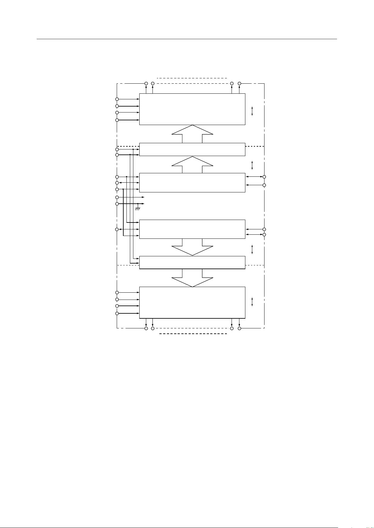
BLOCK DIAGRAM
MSM6648¡ Semiconductor
V
1R
V
2R
V
5R
V
EER
DF
DISP OFF
SHL
IO
CP
V
DD
V
SS
IO
51
O
O
2
1
50-BIT 4-LEVEL DRIVER
O
O
49
50
V
DD
V
EE
50-Bit LEVEL SHIFTER
V
DD
V
SS
IO
1
50-Bit BIDIRECTIONAL SHIFT REGISTER
50-Bit BIDIRECTIONAL SHIFT REGISTER
V
DD
V
50-Bit LEVEL SHIFTER
SS
50
MODE2
MODE1
IO
100
V
1L
V
2L
V
5L
V
EEL
O
51
50-BIT 4-LEVEL DRIVER
O
52
O
V
DD
V
EE
O
99
100
2/9
Page 3
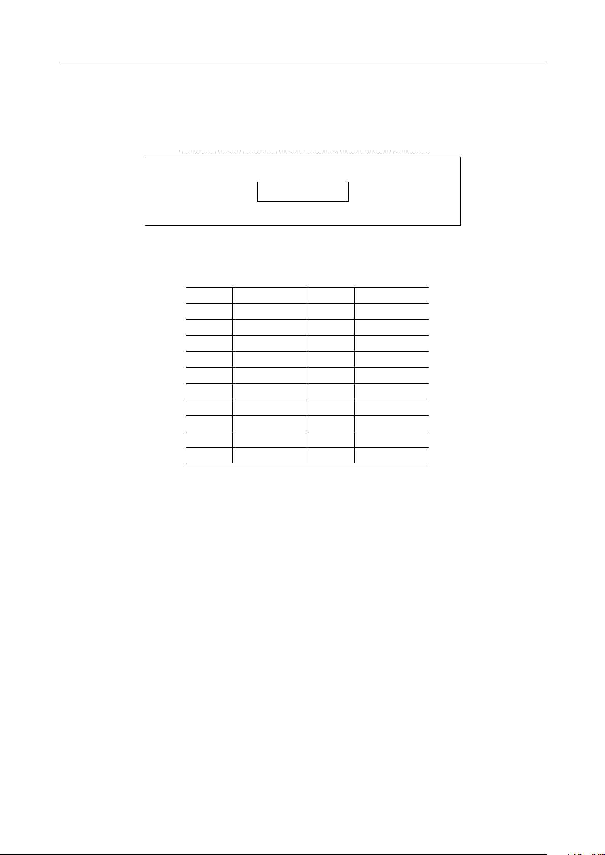
PIN CONFIGURATION (TOP VIEW)
MSM6648¡ Semiconductor
O
100O99
Surface of chip
(LCD output side)
1
234567891011121314151617181920
(Input pin side)
Pin Symbol Pin Symbol
111
212
313
414
515
616
717
818
919
10 20
V
1L
V
2L
V
5L
V
EEL
IO
V
DF
CP
MODE1 IO
IO
100
MODE2
DISP OFF V
V
DD
V
SHL V
IO
51
V
50
SS
1
EER
5R
2R
1R
O2O
1
3/9
Page 4

ABSOLUTE MAXIMUM RATINGS
Parameter Symbol Condition Rating Unit
Power Supply Voltage (1)
Power Supply Voltage (2)
Input Voltage V
Storage Temperature T
V
DD
Ta = 25°C –0.3 to +6.5 V
VDD–VEE *1 Ta = 25°C 0 to 30 V
I
STG
Ta = 25°C –0.3 to VDD + 0.3 V
— –30 to +85 °C
MSM6648¡ Semiconductor
*1 V1 > V2 > V5 > VEE, V
V1 = V1L = V1R, V2 = V2L = V2R, V5 = V5L= V5R, VEE = V
DD
≥ V
> V
1
≥ V
2
– 10V, V
DD
+ 10V ≥ V
EE
EEL
= V
> V
5
EER
EE
RECOMMENDED OPERATING CONDITIONS
Parameter Symbol Condition Range Unit
Power Supply Voltage (1)
Power Supply Voltage (2)
Operating Temperature Top — –20 to +75 °C
*1 V1 > V2 > V5 > VEE, V
V1 = V1L = V1R, V2 = V2L = V2R, V5 = V5L= V5R, VEE = V
V
DD
VDD – VEE *1
≥ V
DD
— 2.7 to 5.5 V
No load 14 to 28 V
During LCD drive 18 to 28 V
> V
1
≥ V
2
– 7V, V
DD
+ 7V ≥ V
EE
EEL
5
= V
> V
EER
EE
4/9
Page 5

ELECTRICAL CHARACTERISTICS
MSM6648¡ Semiconductor
DC Characteristics
(VDD = 2.7 to 5.5V, Ta = –20 to +75°C)
Parameter Symbol Condition Min. Typ. Max. Unit
"H" Input Voltage V
"L" Input Voltage V
"H" Input Current I
"L" Input Current I
"H"
Output Voltage
Output Voltage
"L"
ON Resistance R
Supply Current
Input Capacitance C
*1 — 0.8V
IH
*1 — V
IL
*1 VI = VDD, VDD = 5.5V — — 1 mA
IH
*1 VI = 0V, VDD = 5.5V — — –1 mA
IL
VOH *2 IO = –0.2mA, VDD = 2.7V VDD – 0.4 — — V
VOL *2 IO = 0.2mA, VDD = 2.7V — — 0.4 V
V
– VEE = 25V,
ON
*4
I
SS
I
EE
I
DD
– VO | = 0.25V *3
| V
N
fCP = 28kHz, VDD = 3.0V
– VEE = 25V, No load
V
DD
f = 1MHz — 5 — pF
*1 Applicable to CP, IO1, IO50, IO
*2 Applicable to IO1, IO50, IO51, IO
DD
SS
——2kW
——50
— — 300
, SHL, DF, DISP OFF, MODE1, MODE2.
100
100
—VDDV
— 0.2V
DD
mA
V
*3 VN = VDD to VEE, V2 = 1/16 (VDD – VEE), V5 = 15/16 (VDD – VEE), VDD = V1, VDD = 4.5V
*4 Applicable to O1 to O
100
Switching Characteristics
(VDD = 2.7 to 5.5V, Ta = –20 to +75°C, CL = 15pF)
Parameter Symbol Condition Min. Typ. Max. Unit
"H", "L" Propagation Delay Time t
Clock Frequency f
CP Pulse Width t
Data Setup Time t
Data Hold Time t
Rise/Fall Time of CP t
Note 1 : When display is controlled by DISPOFF pin, CP rise and fall time must be £ 1 ms.
t
WCP
DD
0.8V
IO
IO
CP
1
51
(IO50)
(IO
100
0.8V
)
DD
t
SETUP
PLH
r (CP)
t
0.8V
0.2V
, t
CP
WCP
SETUP
HOLD
, t
f(CP)
DD
DD
PHL
f (CP)
0.2V
t
HOLD
DD
0.8V
0.2V
DD
DD
—
—
—
—
—
—
t
r(CP)
0.2V
—— 3 ms
— — 1 MHz
63——ns
100 — — ns
100 — — ns
——20ns
0.8V
DD
DD
IO
IO
50
100
(IO1)
(IO51)
t
PLH
(t
)
PHL
0.8V
DD
0.2V
DD
5/9
Page 6

FUNCTIONAL DESCRIPTION
Pin Functional Description
MSM6648¡ Semiconductor
• IO, IO50, IO51, IO
100
These are I/O pins for the two 50-bit bidirectional shift registers.
• SHL
This is an input pin to select the shift direction of the two 50-bit bidirectional shift registers.
Set this pin to "H" or "L" level during power-on.
• MODE1, MODE2
These are input pins to select whether the two 50-bit shift registers are used as a two 50-bit
application or a 40-bit and 50-bit application.
Functions of the SHL, MODE1 and MODE2 pins are shown below.
L— L
O51 Æ O
HL —
O
L— H
O
HH —
Scan
direction
O
Æ O
1
O50 Æ O
Æ O
100
O
Æ O
11
Æ O
51
O
Æ O
50
O
Æ O
90
50
100
1
51
50
100
1
51
Data
input pin
IO
1
IO
51
IO
50
IO
100
IO
1
IO
51
IO
50
IO
100
Scan
output pin
IO
50
IO
100
IO
1
IO
51
IO
50
IO
100
IO
1
IO
51
FunctionMODE2MODE1SHL
The scan data input into the IO1, and IO51 pins are
shifted at the falling edge of CP and are output from the
and IO
IO
50
The scan data input into the IO
pins after the lapse of 50 clock pulses.
100
and IO50 pins are
100
shifted at the falling edge of CP and are output from the
and IO1 pins after 50 clock pulses.
IO
51
This condition means a mode of bypassing between the
and O10 pins. The scan data input into the IO1 pin is
O
1
stored in the O
after 40 clock pulses. The operation in the O
pin and is output from the IO50 pin
11
51
pins is the same as that in setting SHL to "L" and MODE2
to "L".
This condition means a mode of bypassing
between the O
input into the IO
and O
91
100
output from the IO
The operation in the O
pins. The scan data
100
pin is stored in O90 and is
pin after 40 clock pulses.
51
to O50 pins is the same as
1
that in setting SHL to "H" and MODE1 to "L".
to O
100
6/9
Page 7

MSM6648¡ Semiconductor
• CP
This is a clock pulse input pin for two 50-bit bi-directional shift registers. Scan data is shifted
at the falling edge of a clock pulse.
• DF
This is an input pin for an LCD drive waveform AC synchronization signal, which generally
inputs a frame inversion signal. See the Truth Table.
• DISP OFF
This is an input pin used to control the output pins O1 to O
output from the output pins O1 to O
, independent of the shift register data during low
100
. Signals on the V1 level are
100
signal input. See the Truth Table.
• O1 to O
100
These are 4-level driver output pins, directly corresponding to each bit of the shift register.
DF signals combined to shift register data select and output any of four levels V1, V2, V5, and
VEE.
• VDD, V
SS
These are power supply pins. VDD is normally 2.7 to 5.5 V. VSS is a grounding pin, which
is normally set to 0 V.
• V1L, V2L, V5L, V
, V1R, V1R, V5R, V
EEL
EER
These are LCD drive bias voltage pins. The V1 pin may be separated from the VDD pin. Bias
supply voltages are supplied from an external source.
Truth Table
DF Shift register data DISP OFF Driver output (O1 to O
LLH V
LHH V
HLH V
HHH V
¥¥LV
2
EE
5
1
1
100
¥ : Don't care
)
NOTES ON USE
Note the following when turning power on and off:
The LCD drivers of this IC requires a high voltage. If a high voltage is applied to them with the
logic power supply floating, excess current flows. This may damage the IC. Be sure to carry out
the following power-on and power-off sequences.
When turning power on:
First turn on the logic circuits, then the LCD drivers, or turn on both of them at the same time.
When turning power off:
First turn off the LCD drivers, then the logic circuits, or turn off both of them at the same time.
7/9
Page 8

APPLICATION CIRCUITS
Example of connecting to LCD panel
In the case of 400 (200 ¥ 2) lines
MSM6648¡ Semiconductor
DATA DATAO
DATA DATAO
1
O
100
O
1
O
100
1st line
100th line
101st line
200th line
O
100
O
1
O
100
O
1
upper screen
lower screen
1
O
100
O
1
1st line
100th line
101st line
O
100
O
1
O
100
O
100
200th line
O
1
8/9
Page 9

In the case of 480 (240 ¥ 2) lines
MSM6648¡ Semiconductor
O
O
DATA
O
O
O
O
O
O
DATA DATA
O
O
O
O
1
10
11
100
1
100
1
50
51
100
1
100
10 pins not used
10 pins not used
1st line
90th line
91st line
190th line
191st line
240th line
1st line
50th line
51st line
150th line
O
100
O
91
O
90
O
1
O
100
O
1
O
100
O
51
O
50
O
1
O
100
O
1
DATA
upper screen
lower screen
O
1
O
90
O
91
10 pins not used
O
100
151st line
240th line
10 pins not used
O
100
O
11
O
10
O
1
9/9
 Loading...