

Page 1

¡ Semiconductor MSM6636
¡ Semiconductor
MSM6636
SAE-J1850 Communication Protocol Conformity Transmission Controller for Automotive LAN
GENERAL DESCRIPTION
The MSM6636 is a transmission controller for automotive LAN based on data communication
protocol SAE-J1850. This LSI can realize a data bus topology bus LAN system with a PWM bit
encoding method (41.6 K bps). In addition to a protocol control circuit, MSM6636 has an enclosed
quartz oscillation circuit, host CPU interface (clock synchronous serial / UART), a transmit/
receive buffer, and a bus receiver circuit that decreases the burden on the host CPU.
FEATURES
• Based on SAE-J1850 CLASS B DATA COMMUNICATION NETWORK INTERFACE (issued
August 12, 1991)
• CSMA/CD (Carrier-sense multiple access with collision detection)
• Internal transmit buffer (1 frame) and receive buffer (2 frames)
• Bit encoding: PWM (Pulse Width Modulation)
• Transmission Speed: 41.6K bps
• Multi-address setting with physical addressing: 1 type / functional addressing: 15 types
• Address filter function by multi-addressing (broadcasting possible)
• Automatic retransmission function by arbitration loss and non ACK
• 3 types of in-frame response support:
q Single-byte response from a single recipient
w Multi-byte response from a single recipient (with CRC code)
e Single-byte response from multiple recipients (ID response as ACK)
• Error detection by cyclic redundancy check (CRC)
• Various communication error detections
• Dual-wire bus abnormality detection by internal bus receiver and fault tolerance function
• Host CPU interface is LSB first / serial, 4 modes supported
q Clock synchronous serial (no parity)
Normal mode: 8-bit data
MPC Mode: 8-bit data + MPC bit (1: address / 0: data select bit)
w UART (yes/no parity selectable)
Normal mode: 1 start bit + 8-bit data + (parity) + 1 stop bit
MPC mode: 1 start bit + 8-bit data + MPC bit + (parity) + 1 stop bit
• Sleep Function
Low current consumption mode by oscillation stop (IDS Max < 50µA)
SLEEP / WAKE UP control from host CPU, WAKE UP via LAN bus
• Available package 18pin DIP, 18 pin QFJ (PLCC) and 24pin SOP.
1
Page 2
MSM6636 ¡ Semiconductor
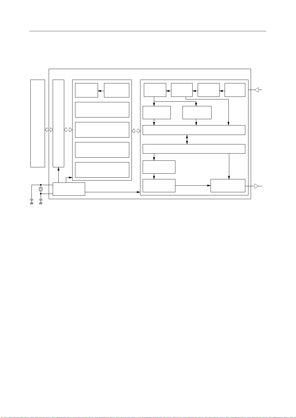
BLOCK DIAGRAM
CPU
x'tal
Receive
Register
Status Register
Serial Interface
Transmission Register
Response Register
Clock
Generator
Buffer Register
Receive
Buffer
Address Register
Converter
Checker
Generator
Converter
MSM6636
S-P
CRC
LAN Controller
PWM
Decoder
Receive Controller
Transmission Controller
CRC
P-S
Address
Filter
Degital
Filter
Bus
Receiver
PWM
Encoder
LAN
Bus
Input
LAN
Bus
Output
2
Page 3
¡ Semiconductor MSM6636
PIN CONFIGURATION (TOP VIEW)
18pin Plastic DIP
1
AVDD DVDD
2
BO– RES
3
BI– INT
4
BI+ TXD
5
BO+ RXD
6
AGND
7
U-C A-D
8
M-N OSC0
9
DGND OSC1
8
1
7
1
6
1
5
1
4
1
3
1
2
1
1
1
0
1
PIN DESCRIPTION
Pin Name I/O Function
AVDD 1 — Analog power supply pin
BO – 2 O LAN - BUS output –
BI – 3 I
BI + 4 I
BO + 5 O
AGND 9 — Analog ground pin
U - C 10 I 0: UART 1: clock synchronous serial select pin
M - N 11 I 0: MPC mode 1:normal mode select pin
DGND 12 — Digital ground pin
OSC 1 13 O Crystal oscillation output
OSC 0 14 I Crystal oscillation input
A - D
SCLK / PAE 16 I Serial clock input/Parity select pin
RXD 20 I Serial data input pin
TXD 21 O Serial data output pin
INT 22 O Interrupt output pin
RES 23 I Reset input pin
DVDD 24 — Digital power supply pin
SCLK
/PAE
18pin Plastic QFJ
BO–M-N
AVDDDGND
DVDDOSC1
11817
2
3
BI– INT
4
BI+ TXD
5
BO+ RXD
6
AGND
7
U-C A-D
8 9 10 11
Pin #
DIP/
SOP
QFJ
1
2
3
4
5
LAN - BUS input –
LAN - BUS input +
LAN - BUS output +
6
7
8
9
10
11
12
15 I
0: data communication
1: address communication
13
14
15
16
17
18
RESOSC0
16
15
14
13
12
24pin Plastic SOP
1
AVDD DVDD
2
BO– RES
3
BI– INT
4
BI+ TXD
5
BO+ RXD
6
NC NC
7
NC NC
8
NC NC
SCLK
/PAE
9
AGND SCLK/PAE
10
U-C A-D
11
M-N OSC0
12
DGND OSC1
NC: No Connection
24
23
22
21
20
19
18
17
16
15
14
13
3
Page 4
MSM6636 ¡ Semiconductor
ABSOLUTE MAXIMUM RATINGS
DGND = AGND = 0V
Parameter Symbol
Power Supply Voltage DVDD, AVDD
Input Voltage V
Output Voltage V
Power Dissipation
Storage Temperature T
P
D(DIP)
P
D(QFJ)
P
D(SOP)
STG
I
O
1
*
2
*
3
*
Condition Rated Value Unit
-0.3~7.0 V
AVDD = DVDD
AVDD = DVDD
-0.3~DVDD+0.3 V
-0.3~DVDD+0.3 V
Ta = 25°C 860 mW
Ta = 25°C 960 mW
Ta = 25°C 830
-55~150 °C
mW
D(DIP)
D(QFJ)
D(SOP)
*1
: 18PIN DIP package power dissipation
*2
: 18PIN QFJ package power dissipation
*3
: 24PIN SOP package power dissipation
P
P
P
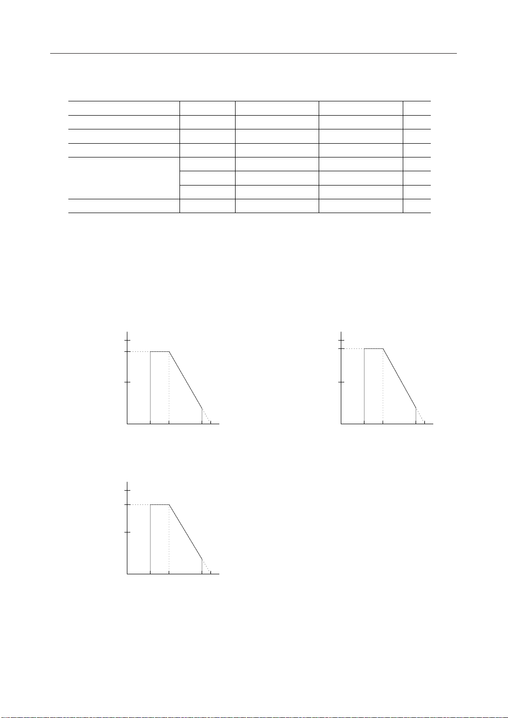
Power Dissipation Curve
< 18PIN DIP package > < 18PIN QFJ package >
1000
860
[mW]
D(DIP)
500
Power dissipation P
1000
[mW]
830
-40 25 125 150
Ambient temperature Ta (°C)
< 24PIN SOP package >
1000
960
[mW]
D(QFJ)
500
-40 25 125 150
Power dissipation P
Ambient temperature Ta (°C)
D(SOP)
500
-40 25 125 150
Power dissipation P
Ambient temperature Ta (°C)
4
Page 5

¡ Semiconductor MSM6636
OPERATION RANGE
DGND = AGND = 0V
Parameter Symbol
Power Supply Voltage DVDD, AVDD
Operating Frequency f
OSC
Operating Temperature Ta
Condition Rated Value Unit
AVDD = DVDD 4.5~5.5 V
DVDD = AVDD = 5V±10% 2~16 MHz
-40~+125 °C
ELECTRICAL CHARACTERISTICS
DC Characteristics
DVDD = AVDD = 5V±10%, DGND = AGND = 0V, Ta = -40 ~ +125°C
Parameter Symbol Condition Application MIN TYP MAX Unit
H Level Input Voltage V
L Level Input Voltage V
H Level Input Voltage V
L Level Input Voltage V
Receiver Hysteresis Width V
H Level Input Current I
L Level Input Current I
H Level Input Current I
L Level Input Current I
H Level Input Current I
L Level Input Current I
H Level Output Voltage V
L Level Output Voltage V
H Level Output Voltage V
L Level Output Voltage V
GND Offset Voltage V
Current Consumption 1 I
Current Consumption 2 I
IH1
IL1
IH2
IL2
H
IH1
IL1
IH2
IL2
IH3
IL3
OH1IO
OL1IO
OH2IO
OL2IO
OFF
DS
DD
— A DVDD ¥ 0.8 — DVDD + 0.3 V
— A DGND - 0.3 — DVDD ¥ 0.2 V
— F DVDD - 2.0 — DVDD + 1.0 V
— F DGND - 1.0 — DGND + 2.0 V
— F 100 — 400 mV
VI = V
DD
B——+ 1µA
VI = 0V B — — - 1 µA
VI = V
DD
C——+ 1µA
VI = 0V C — — - 100 µA
VI = V
DD
BI (+) — — + 100 µA
VI = 0V BI (-) — — - 100 µA
= -400µA D DVDD - 0.4 — — V
= +3.2mA D — — DGND + 0.4 V
= -4.0mA E DVDD - 0.4 — — V
= +4.0mA E — — DGND + 0.4 V
—
During sleep — — 50 µA
f = 16MHz,
no load
—
—
——±1 V—
——10mA
A: RES, SCLK/PAE, RXD, U-C, M-N, A-D, OSC0
B: SCLK/PAE, RXD, U-C, M-N, A-D
C: RES
D: TXD, INT
E: BO-, BO+
F: BI-, BI+
5
Page 6

MSM6636 ¡ Semiconductor
AC Chacteristics
PWM Bit Timing
Parameter Symbol
Bit Length TP1
"1" Dominant Width TP2
"0" Dominant Width TP3
"SOF" Dominant Width TP4
"SOF,BRK" Length TP5
"BRK" Dominant Width TP6
"EOD" + Bit Length TP7
"EOF" + Bit Length TP8
min typ max min max
23.64 24.00 24.36 21.00 28.00 µs
14.87 15.00 15.23 13.00 20.00 µs
30.54 31.00 31.47 29.00 36.00 µs
47.28 48.00 48.72 45.00 52.00 µs
38.42 39.00 39.59 37.00 44.00 µs
47.28 48.00 48.72 43.00 51.00 µs
70.92 72.00 — 69.00 76.00 µs
Transmit Receive
6.90 7.00 7.11 5.00 12.00 µs
"EOF + IFS" + Bit Length TP9 94.56 96.00 — 86.00 — µs
"0" Passive Width TP10
8.86 9.00 9.14 4.00 15.00 µs
Note: DVDD = AVDD = 5 V ± 10%, Ta = -40 ~ +125˚C, In setting 41.6 K bps
Dominant
" 1 "
Passive
Dominant
" 0 "
Passive
TP2
TP3
TP1
Unit
TP10
TP4
TP5
EOD
TP7
EOF IFS
TP8
TP9
TP6
TP5
" SOF "
" EOD "
" EOF "
" IFS "
" BRK "
Dominant
Passive
Dominant
Passive
LAST BIT
Dominant
Passive
LAST BIT
Dominant
Passive
6
Page 7

¡ Semiconductor MSM6636
CPU Serial Interface Timing
mClock synchronous Serial
DVDD=AVDD=5V±10%, Ta =-40~+125°C
Parameter Symbol Min Typ Max Unit
OSCO (source oscillation) Pulse Cycle tø 62 500 ns
SCLK-L Interval Width t
SCLK-H Interval Width t
SCLK ≠ - RXD Setup Time t
SCLK ≠ - RXD Hold Time t
SCLK ≠ - TXD Output Delay Time t
A-D - SCLK ≠ Setup Time t
SCLK ≠ - A-D Hold Time t
SCLK Frame Interval Time *1 t
SCLK Frame Interval Time *2 t
SCLK Frame Interval Time
*1
CKLW
CKHW
SRS
SRH
STD
AS
AH
INT1
INT2
16tø — ns
—
8tø — ns
—
—
8tø — ns
4tø — ns
—
—
4tø — ns
4tø 6tø + 100 ns
—
0—ns
—
—
8tø — ns
8tø — ns
—
—
Between “Communication type (WR) and address setting” frame and “WR data” frame.
Between “WR data” frame and “WR data” frame during continuous WR.
SCLK Frame Interval Time
*2
Between “Communication type (RD) and address setting” frame and “RD data” frame.
Between “RD data” frame and “RD data” frame during continuous RD.
7
Page 8

MSM6636 ¡ Semiconductor
mUART
DVDD=AVDD=5V±10%, Ta =-40~+125°C
Parameter Symbol Min Typ Max Unit
A-D - STOP bit ≠ Setup Time t
STOP bit Ø – A-D Hold Time t
START bit Ø – TXD Output Delay Time t
Write Frame Interval Time *3 t
Read Frame Interval Time *4 t
UAS
UAH
UTD
INT3
INT4
48tø 50tø + 100 ns
10tø — ns
—
0—ns
0—ns
—
—
—
0—ns
—
Write Frame Interval Time
*3
Between “Communication type (WR) and address setting” frame and “WR data” frame.
Between “WR data” frame and “WR data” frame during continuous WR.
Read Frame Interval Time
*4
Between “Communication type (RD) and address setting” frame and “RD data” frame.
8
Page 9

¡ Semiconductor MSM6636
Wakeup Input Signal
DVDD=AVDD=5V±10%, Ta =-40~+125°C
Parameter Symbol Min Typ Max Unit
LAN bus Passive Æ Dominant Change Pulse Width t
RXD Terminal Input Pulse Width t
Bus Receiver Stable Time *5 t
tø
OSC0
t
UAS
A-D
WD
WR
RS
300 — ns
t
UAH
—
7—µs
—
1—µs
—
RXD
TXD
STOP
t
INT3
t
INT4
START
t
UTD
START
STOP bit Termination
Note: The time chart shows the wakeup input signals from each sleep status
Bus Receiver Stable Time
*5
The stable time of the bus receiver is from just after wakeup to the restart of message transmission and reception. However, the clock oscillation source should use an external clock.
(A clock is input even in the sleep status.)
9
Page 10

MSM6636 ¡ Semiconductor
Fault Tolerant Function Operation Conditions
DVDD=AVDD=5V±10%, Ta =-40~+125°C, In setting 41.6Kbps
Parameter Symbol Min Typ Max Unit
LAN bus (+) GND Short Circuit Detection Pulse Width t
LAN bus (+) VDD Short Circuit Detection Pulse Width t
LAN bus (-) GND Short Circuit Detection Pulse Width t
LAN bus (-) VDD Short Circuit Detection Pulse Width t
BUS(+)
BUS(-)
t
PG
BUS(+)
BUS(-)
PG
PV
NG
NV
—
5—µs
—
48 — µs
48 — µs—
5—µs
—
t
PV
t
NV
Reset Input Pulse Width
Parameter Symbol Min Typ Max Unit
Reset Input Pulse Width t
RES
t
RES
t
NG
DVDD=AVDD=5V±10%, Ta=–40~+125°C
0.1 — µs
RES
—
10
Page 11

¡ Semiconductor MSM6636
APPLICATION EXAMPLE
Host CPU and LAN bus Connection Example
Host CPU and LAN bus connection example of MSM6636 is shown below.
Unit A
MSM6636Host CPU
AVDDDVDD
SOUT RXD
SIN TXD BO (+)
INT INT
CLKOUT OSC0 BI (+)
OPEN
OSC1
SCLK / PAE BI (-)
U - C
M - N BO (-)
A - D
AGNDDGNDRESRES
ZD
ZD
Unit B
.
.
.
Bus + Bus -
The above connection example is when "UART, MPC and parity no mode" was used as the
"host CPU interface, and when CLKOUT output of the host CPU" was used as the clock for
MSM6636.
Depending on the control target, an optimum host CPU (number of ports, A/D converter yes
/ no) can be selected, and an optimum system can be constructed.
11
 Loading...