

Datasheet MSM66201-xxxSS, MSM66201-xxxGSBK, MSM66207-xxxSS, MSM66207-xxxGSBK, MSM66P207-xxxSS Datasheet (OKI)
...Page 1

E2E1027-27-Y4
¡ Semiconductor MSM66201/66P201/66207/66P207
¡ Semiconductor
This version: Jan. 1998
Previous version: Nov. 1996
MSM66201/66P201/66207/
66P207
OLMS-66K Series 16-Bit Microcontroller
GENERAL DESCRIPTION
The MSM66201/66207 is a high performance microcontroller that employs OKI original nX-8/
200 CPU core. This chip includes a 16-bit CPU, ROM, RAM, I/O ports, multifunction 16-bit
timers, 10-bit A/D converter, serial I/O port, and pulse width modulator (PWM). The
MSM66P201/66P207 is the OTP (One-Time Programmable) version of the MSM66201/66207.
FEATURES
• 64K address space for program memory : Internal ROM : MSM66201 16K bytes
MSM66207 32K bytes
• 64K address space for data memory : Internal RAM : MSM66201 512 bytes
MSM66207 1024 bytes
• High-speed execution
Minimum cycle for instruction : 400ns @ 10MHz
• Powerful instruction set : Instruction set superior in orthogonal matrix
8/16-bit data transfer instructions
8/16-bit arithmetic instructions
Multiplication and division operation instructions
Bit manipulation instructions
Bit logic instrucitons
ROM table reference instructions
• Abundant addressing modes : Register addressing
Page addressing
Pointing register indirect addressing
Stack addressing
Immediate value addressing
• I/O port
Input-output port : 5 ports ¥ 8 bits
(Each bit can be assigned to input or output)
Input port : 1 port ¥ 8 bits
• Built-in multifunctional 16-bit timer : 4
Following 4 modes can be set for each timer : Auto-reload timer mode
Clock output mode
Capture register mode
Real time output mode
• Serial port : 1 channel (Synchronous/UART switchable
mode with baud rate generators)
• 16-bit pulse width modulator : 2
• Watchdog timer
• Transition detector : 4
• 10-bit A/D converter : 8 channels
• Interrupts
Nonmaskable : 1
Maskable : Internal 16/external 2
• Stand-by function
STOP mode : Software clock stop mode
HALT mode : Software CPU stop mode
HOLD mode : Hardware CPU stop mode
1/30
Page 2

¡ Semiconductor MSM66201/66P201/66207/66P207
• Package
64-pin plastic shrink DIP (SDIP64-P-750-1.78)
64-pin plastic QFP (QFP64-P-1414-0.80-BK)
68-pin plastic QFJ (PLCC) (QFJ68-P-S950-1.27)
64-pin ceramic piggyback (ADIP64-C-750-1.78)
* The piggyback type is used only for engineering samples.
: (MSM66201-¥¥¥SS) (MSM66P201-¥¥¥SS)
(MSM66207-¥¥¥SS) (MSM66P207-¥¥¥SS)
: (MSM66201-¥¥¥GSBK)(MSM66207¥¥¥GS-
BK)
: (MSM66201-¥¥¥JS) (MSM66P201-¥¥¥JS)
(MSM66207-¥¥¥JS) (MSM66P207-¥¥¥JS)
: (MSM66G207VS)
(¥¥¥ indicates the code number.)
2/30
Page 3
¡ Semiconductor MSM66201/66P201/66207/66P207
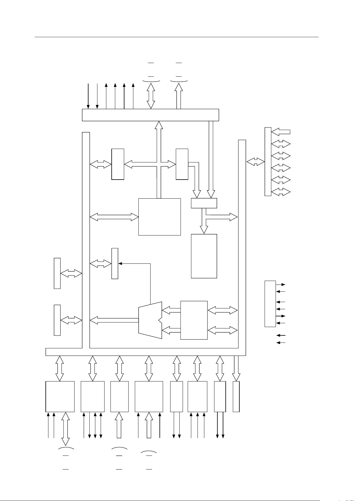
BLOCK DIAGRAM
EA
READY
ALE
PSENRDWR
AD0/P0.0
AD7/P0.7
A8 /P1.0
A15/P1.7
BUS P
*2
RAM
PSW
O
R
1024 ¥ 8 bits
T
C
O
N
CONT.
MEMORY
.
T
ROM
32K ¥ 8 bits
*1
IR
PC
RAP
DECODER
INSTRUCTION
*1 MSM66201 16K ¥ 8
PORT
*2 MSM66201 512 ¥ 8
P5
P4
P3
P2
P1
P0
HLDA/P2.5
HOLD/P2.4
SSP LRB
0–3
TIMER
P4.0/TM0CK
P4.1/TM1CK
P3.4/TM0IO
SERIAL
P3.7/TM3IO
P3.1/RXD
P3.0/TXD
PORT
P2.7/RXC
P2.6/TXC
TION D.
TRANSI-
P4.4/TRNS0
P4.7/TRNS3
A/D
REF
V
P5.0/AI 0
ALU
CONV.
P5.7/AI 7
AGND
ALU CONT.
0,1
PWM
NMI
P4.2/PWM0
P4.3/PWM1
R.
ACCUMULATOR
TEMPORARY
CONSTANTS
CONT.
INTERRUPT
P3.2/INT0
P3.3/INT1
CONT.
PERIPHERAL
RESOUT
P2.3/CLKOUT
WDT
FLT
RES
CONTROLLER
SYSTEM
OSC1
OSC0
GND
V
DD
3/30
Page 4
¡ Semiconductor MSM66201/66P201/66207/66P207
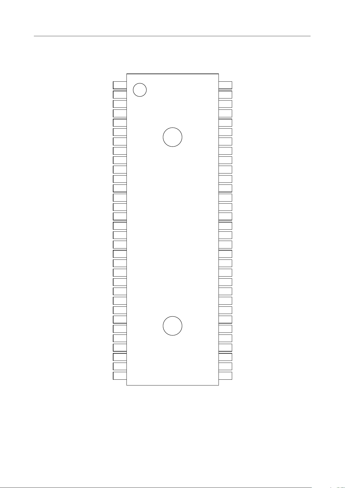
PIN CONFIGURATION (TOP VIEW)
AD0/P0.0
AD1/P0.1
AD2/P0.2
AD3/P0.3
AD4/P0.4
AD5/P0.5
AD6/P0.6
AD7/P0.7
A8/P1.0
A9/P1.1
A10/P1.2
A11/P1.3
A12/P1.4
A13/P1.5
A14/P1.6
A15/P1.7
P2.0
P2.1
P2.2
CLKOUT/P2.3
RESOUT P3.6/TM2IO
ALE P3.5/TM1IO
PSEN P3.4/TM0IO
RD P3.3/INT1
WR P3.2/INT0
READY P3.1/RXD
FLT P2.7/RXC
RES P2.6/TXC
OSC0 P2.5/HLDA
OSC1 P2.4/HOLD
GND NMI
1
2
3
4
5
6
7
8
9
10
11
12
13
14
15
16
17
18
19
20
21
22
23
24
25
26
27
EA P3.0/TXD
28
29
30
31
32
64
63
62
61
60
59
58
57
56
55
54
53
52
51
50
49
48
47
46
45
44
43
42
41
40
39
38
37
36
35
34
33
V
DD
V
REF
AGND
P5.7/AI7
P5.6/AI6
P5.5/AI5
P5.4/AI4
P5.3/AI3
P5.2/AI2
P5.1/AI1
P5.0/AI0
P4.7/TRNS3
P4.6/TRNS2
P4.5/TRNS1
P4.4/TRNS0
P4.3/PWM1
P4.2/PWM0
P4.1/TM1CK
P4.0/TM0CK
P3.7/TM3IO
64-Pin Plastic Shrink DIP
4/30
Page 5
¡ Semiconductor MSM66201/66P201/66207/66P207
PIN CONFIGURATION (TOP VIEW) (Continued)
A8/P1.0
A9/P1.1
A10/P1.2
A11/P1.3
A12/P1.4
A13/P1.5
A14/P1.6
A15/P1.7
P2.0
P2.1
P2.2
10
11
12CLKOUT/P2.3
13RESOUT
14ALE
15PSEN
16RD
P0.7/AD7
P0.6/AD6
P0.5/AD5
P0.4/AD4
P0.3/AD3
P0.2/AD2
P0.1/AD1
64
63
62
61
60
59
58
1
2
3
4
5
6
7
8
9
DDVREF
P0.0/AD0
V
57
56
55
AGND
54
53 P5.7/AI7
52 P5.6/AI6
54 P5.5/AI5
50 P5.4/AI4
49 P5.3/AI3
48
P5.2/AI2
47
P5.1/AI1
46
P5.0/AI0
45
P4.7/TRNS3
44
P4.6/TRNS2
43
P4.5/TRNS1
42
P4.4/TRNS0
41
P4.3/PWM1
40
P4.2/PWM0
39
P4.1/TM1CK
38
P4.0/TM0CK
37 P3.7/TM3IO
36 P3.6/TM2IO
35 P3.5/TM1IO
34 P3.4/TM0IO
33 P3.3/INT1
17
WR
18
19
EA
READY
20
21
22
23
24
FLT
RES
OSC0
OSC1
GND
64-Pin Plastic QFP
25
26
NMI
HOLD/P2.4
27
28TXC/P2.6
29RXC/P2.7
HLDA/P2.5
30TXD/P3.0
31RXD/P3.1
32INT0/P3.2
5/30
Page 6
¡ Semiconductor MSM66201/66P201/66207/66P207
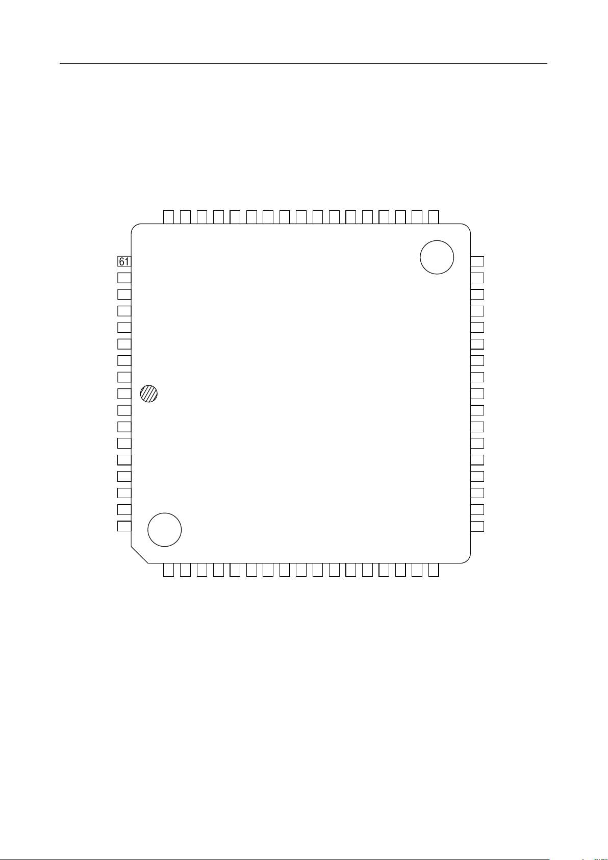
PIN CONFIGURATION (TOP VIEW) (Continued)
P5.2/AI2
P5.1/AI1
P5.0/AI0
P4.7/TRNS3
P4.6/TRNS2
P4.5/TRNS1
P4.4/TRNS0
60
59
58
57
56
55
P4.3/PWM1
54
53
P4.1/TM1CK
52
51
P4.0/TM0CKNCP3.7/TM3IO
50
49
P3.6/TM2IO
48
47
P3.5/TM1IO
46
P3.4/TM0IO
P3.3/INT1
45
44
AI3/P5.3
AI4/P5.4
AI5/P5.5
AI6/P5.6
AI7/P5.7
AGND
V
REF
V
DD
V
DD
AD0/P0.0
AD1/P0.1
AD2/P0.2
AD3/P0.3
AD4/P0.4
AD5/P0.5
AD6/P0.6
AD7/P0.7
61
62
63
64
65
66
67
68
P3.2/INT0
43
P3.1/RXD
42
P3.0/TXD
41
P2.7/RXC
40
P2.6/TXC
39
P2.5/HLDA
38
P2.4/HOLD
37
NMI
36
1
2
3
4
5
6
7
8
9
35
34
33
32
31
30
29
28
27
GND
GND
OSC1
OSC0
RES
FLT
EA
READY
WR
10
11
A8/P1.0
A9/P1.1
12
13
14
15
16
17
18
NC P4.2/PWM0
A10/P1.2
A11/P1.3
A12/P1.4
A13/P1.5
A14/P1.6
A15/P1.7
NC : No-connection pin
68-Pin Plastic QFJ (PLCC)
19
P2.0
20
P2.1
21
22
P2.2
RESOUT
CLKOUT/P2.3
23
24
ALE
25
PSEN
26
RD
6/30
Page 7

¡ Semiconductor MSM66201/66P201/66207/66P207
PIN DESCRIPTION
Type DescriptionSymbol
P0.0–P0.7/
AD0–AD7
I/O
P0: 8-bit input-output port. Each bit can be assigned to input or output.
AD: Outputs the lower 8 bits of program counter during external program memory fetch,
and receives the addressed instruction under the control of PSEN. This pin also
outputs the address and outputs or inputs data during an external data memory
access instruction, under the control of ALE, RD, and WR.
P1.0–P1.7/
A8–A15
I/O
P1: 8-bit input-output port. Each bit can be assigned to input or output.
A: Outputs the upper 8 bits of program counter (PC
) during external program
8–15
memory fetch. This pin also outputs the upper 8 bits of address during external
data memory access instructions.
P2.0–P2.2
I/O
P2: 8-bit input-output port. Each bit can be assigned to input or output.
P2.3/CLKOUT CLKOUT: Output pin for supplying a clock to peripheral circuits.
P2.4/HOLD
P2.5/HLDA
HOLD: Input pin to request the CPU to enter the hardware power-down state.
HLDA: HOLD ACKNOWLEDGE: the HLDA signal appears in response to the HOLD
signal and indicates that the CPU has entered the power-down state.
P2.6/T
P2.7/R
P3.0/T
P3.1/R
P3.2/INT0 R
C
X
CR
X
D
X
D
X
I/O
C: Transmitter clock input/output pin.
T
X
C: Receiver clock input/output pin.
X
P3: 8-bit input-output port. Each bit can be assigned to input or output.
TXD: Transmitter data output pin.
D: Receiver data input pin.
X
P3.3/INT1 INT: Interrupt request input pin.
P3.4/TM0IO
P3.5/TM1IO
P3.6/TM2IO
P3.7/TM3IO
Falling edge trigger or level trigger is selectable.
TM0IO-TM3IO: One of the following signals is output or input.
• Clock at twice the frequency range of the 16-bit timer overflow
• Load trigger signal to the capture register input
• Setting value output
Whether the signal is input or output depends on the mode.
P4.0/TM0CK P4: 8-bit input-output port. Each bit can be assigned to input or output.
I/O
P4.1/TM1CK TM0CK, TM1CK: Clock input pins of timer 0, timer 1.
P4.2/PWM0
P4.3/PWM1
P4.4
– P4.7/
TRANS: Transition detector.
The input pins which sense the falling edge and set the flag.
PWM: 16-bit pulse-width modulator output pin.
TRANS0 –
TRANS3
P5.0 – P5.7/
AI0 –AI7
I
P5: 8-bit input port.
AI: Analog signal input pin for A/D converter.
7/30
Page 8

¡ Semiconductor MSM66201/66P201/66207/66P207
PIN DESCRIPTION (Continued)
Type DescriptionSymbol
RESOUT
O
Outputs "H" level in the case of internal reset.
Reset to"L" level by program.
ALE
PSEN Program Strobe Enable:
RD Output strobe activated during a bus read cycle.
WR Output strobe during a bus write cycle.
EA Normaly set to "H" level.
FLT If FLT is "H" level, ALE, WR, RD, PSEN are set to "H" level when reset.
RES RESET input pin.
OSC0
OSC1
NMI Non-maskable interrupt input pin (falling edge).
V
REF
AGND Ground for A/D converter.
V
DD
GND Ground.
O
O
O
O
IREADY Used when the CPU accesses low-speed peripherals.
I
I
I
I
O
I
—
—
—
—
Address Latch Enable:
Used to enable data onto the bus from the external data memory.
Used as write strobe to external data memory.
If set to "L" level, the CPU fetches the code from external program memory.
If FLT is set to "L", ALE, WR, RD, PSEN are set to floating level when reset.
Basic clock oscillation pin.
Basic clock oscillation pin.
Reference voltage input pin for A/D converter.
System power supply.
The timing pulse to latch the lower 8 bits of the address
output from port 0 when the CPU accesses the external
memory.
The strobe pulse to fetch to external program
memory.
8/30
Page 9
¡ Semiconductor MSM66201/66P201/66207/66P207
REGISTERS
Accumulator
15 0
ACC
Control Register (CR)
15 0
PSW
Bit 15 : Carry flag (CY)
Bit 14 : Zero flag (ZF)
Bit 13 : Half carry flag (HC)
Bit 12 : Data descriptor (DD)
Bit 8 : Master interrupt priority flag (MIP)
Bit 9,5,4: User flag (MIP)
Bit 2-0
: System control base 2-0 (SCB2-0)
15 0
PC
Pointing Register (PR)
Index Register 1
Index Register 2
Data Pointer
User Stack Pointer
Local Register
LRB
SSP
15 0
X1
X2
DP
USP
7070
ER0
ER1
ER2
ER3
R1
R3
R5
R7
R0
R2
R4
R6
9/30
Page 10

¡ Semiconductor MSM66201/66P201/66207/66P207
SFR
Address
(HEX)
0000
0001
0002
0003
0004I
0005I
0006
0007
0010I
0011
0012I
0013
0018
0019
001A
001B
001CI
0020
0021
0022
0023
0024
0025
0026I
0028
0029
002A
002C
002D
002E
002F
0030
0031
0032
0033
0034
0035
0036
0037
Name Symbol R/W
System stack printer
Local register base
Program status word
Accumulator
Standby control register
Watchdog timer
Peripheral control register
Stop code acceptor
Interrupt request register
Interrupt enable register
External Iinterrupt control register
Port 0 data register
Port 0 mode register
Port 1 data register
Port 1 mode register
Port 2 data register
Port 2 mode register
Port 2 secondary function control register
Port 3 data register
Port 3 mode register
Port 3 secondary function control register
Port 4 data register
Port 4 mode register
Port 4 secondary function control register
Port 5
Timer 0 counter
Timer 0 register
Timer 1 counter
Timer 1 register
SSP
(ASSP)
LRB
(ALRB)
PSWL
(APSW)
PSWH
ACC
SBYCON
WDT
PRPHF
STPACP
IRQ
IE
EXICON
P0
P0IO
P1
P1IO
P2
P2IO
P2SF
P3
P3IO
P3SF
P4
P4IO
P4SF
P5
TM0
TMR0
TM1
TMR1
8/16-bit
Operation
R/W
8/16
W
R/W
W
8/16
R/W
R
R/W 16
Reset
FFH
FFH
undefined
C8H
0CH
00H
00H
F8H
00H/WDT
8
is stopped
FDH
"0"
00H
00H
00H
00H
FCH
undefined
00H
undefined
00H
undefined
8
00H
07H
undefined
00H
00H
undefined
00H
00H
—
00H
00H
00H
00H
00H
00H
00H
00H
Note: A I mark in the address column indicates that there is a bit that does not exist in the
register.
10/30
Page 11

¡ Semiconductor MSM66201/66P201/66207/66P207
SFR (Continued)
Addres
(HEX)
0038
0039
003A
003B
003C
003D
003E
003F
0040
0041
0042
0043
0046I
0048
0049
004AI
004C
004D
004EI
0050I
0051
0054
0055
0056I
0058I
0059I
0060I
0061
Name
Timer 2 counter
Timer 2 register
Timer 3 counter
Timer 3 register
Timer 0 control register
Timer 1 control register
Timer 2 control register
Timer 3 control register
Transition detector register
Serial port transmission baud rate generator counter
Serial port transmission baud rate generator register
Serial port transmission baud rate generator control
register
Serial port receiving baud rate generator counter
Serial port receiving baud rate generator register
Serial port receiving baud rate generator control
register
Serial port transmission mode control register
Serial port transmission data buffer register
Serial port receiving mode control register
Serial port receiving data buffer register
Serial port receiving error register
A/D scan mode register
A/D select mode register
A/D conversion result register 0
Abbreviated
Name
TM2
TMR2
TM3
TMR3
TCON0
TCON1
TCON2
TCON3
TRNSIT
STTM
STTMR
STTMC
SRTM
SRTMR
SRTMC
STCON
STBUF
SRCON
SRBUF
SRSTAT
ADSCAN
ADSEL
ADCR0
R/W
R/W
W
R/W
R
R/W
R
8/16-bit
Operation
16
undefined
8
undefined
undefined
8/16 undefined
Reset
00H
00H
00H
00H
00H
00H
00H
00H
00H
00H
00H
00H
00H
00H
0CH
00H
00H
0EH
80H
00H
F0H
80H
A0H
Note: A I mark in the address column indicates that there is a bit that does not exist in the
register.
11/30
Page 12

¡ Semiconductor MSM66201/66P201/66207/66P207
SFR (Continued)
Address
(HEX)
0062I
0063
0064I
0065
0066I
0067
0068I
0069
006AI
006B
006CI
006D
006EI
006F
0070
0071
0072
0073
0074
0075
0076
0077
0078
007A
Name
A/D conversion result register 1
A/D conversion result register 2
A/D conversion result register 3
A/D conversion result register 4
A/D conversion result register 5
A/D conversion result register 6
A/D conversion result register 7
PWM 0 counter
PWM 0 register
PWM 1 counter
PWM 1 register
PWM 0 control register
PWM 1 countrol register
Abbreviated
Name
ADCR1
ADCR2
ADCR3
ADCR4
ADCR5
ADCR6
ADCR7
PWMC0
PWMR0
PWMC1
PWMR1
PWCON0
PWCON1
R/W
R
R/W
8/16-bit
operation
8/16
8
Reset
undefined
00H
00H
00H
00H
00H
00H
00H
00H
00H
00H
Note: A I mark in the address column indicates that there is a bit that does not exist in the
register.
12/30
Page 13

¡ Semiconductor MSM66201/66P201/66207/66P207
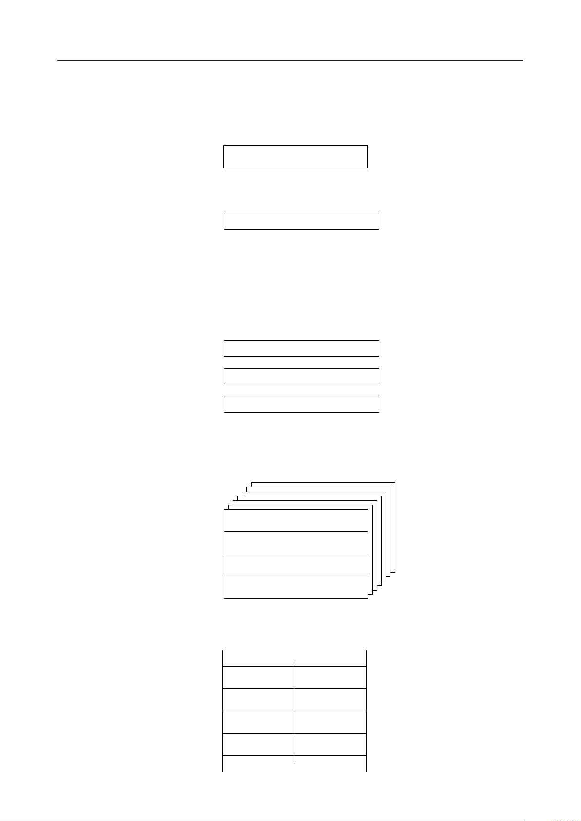
ADDRESSING MODES
The MSM66201/66207 provides independent 64K-byte data and 64K-byte program space with
various types of addressing modes. These modes are shown below, for both RAM (for data space)
and ROM (for program space).
1. RAM Addressing Modes (for data space)
1.1 Register Direct Addressing
Example
ROR
1.2 Displacement Addressing
a) Zero Page
Example
L
A,
b) Direct Page
Example
ST
A,
DP
18H
off 10H
DP
0000H
SFR
0018H
xx00H
RAM
xx10H
1.3 Pointing Register (PR) Indirect Addressing
a) Data Point (DP) Indirect
Example
SLL
[DP]
DP
RAM
b) User Stack Pointer (USP) Indirect
Example
SRL
10H
[USP]
USP
–128 to +127
RAM
13/30
Page 14

¡ Semiconductor MSM66201/66P201/66207/66P207
c) Index Register (X1, X2) Indirect
Example
INC 300H
[X1]
RAM
X1
0 to 65535
1.4 Immediate Addressing
Example
MOV
#27FHSSP,
2. ROM Addressing Modes (for program space)
2.1 Direct Addressing
Example
LC A,
200H
2.2 Simple Indirect Addressing
a) Local Register Indirect
Example
LC
A,
[ER0]
ER0
b) Pointing Register Indirect
1) Data Pointer (DP) Indirect
Example
LC
A,
[DP]
DP
ROM
0200H
ROM
ROM
2) User Stack Pointer (USP) Indirect
Example
LC
[USP]
A,
USP
ROM
14/30
Page 15

¡ Semiconductor MSM66201/66P201/66207/66P207
3) Index Register (X1, X2) Indirect
Example
LC
A,
[X1]
X1
ROM
c) System Stack Pointer (SSP) Indirect
Example
[SSP]LC
A,
SSP
ROM
d) Local Register Base (LRB) Indirect
Example
LC
A,
[LRB]
LRB
ROM
e) RAM Indirect
Example
A, [0C0H]J
RAM
2.3 Double Indirect Addressing
a) Data Pointer (DP) Double Indirect
Example
[[DP]]J
RAM
DP
b) User Stack Pointer (USP) Double Indirect
Example
LC
A, [–2 [USP]]
USP
0C0H
RAM
ROM
ROM
ROM
–128 to +127
15/30
Page 16

¡ Semiconductor MSM66201/66P201/66207/66P207
c) Index Register (X1, X2) Double Indirect
Example
LC
A, [10000H [x1]]
RAM
ROM
X1
0 to 65535
2.4 Indirect Addressing with 16-bit Offset
a) Pointing Register Indirect
1) Data Pointer (DP) Indirect
Example
LC A, [100H [DP]]
DP
0 to 65535
ROM
2) User Stack Pointer (USP) Indirect
Example
LC
A, [100H [USP]]
USP
0 to 65535
3) Index Register (X1, X2) Indirect
Example
LC A, [100H [X1]]
X1
0 to 65535
b) RAM Indirect
Example
LC A, [2000H [80H]]
ROM
ROM
RAM
80H
0 to 65535
ROM
16/30
Page 17

¡ Semiconductor MSM66201/66P201/66207/66P207
MEMORY MAPS
Program Memory Space
0000H
7FFFH *
FFFFH
Internal
ROM Area
External
Memory
* MSM66201 : 3FFFH
0000H
0027H
0028H
0037H
0038H
7FFFH *
Vector
Table
Area
(40 bytes)
VCAL
Table
Area
(16 bytes)
Data Memory Space
0000H
007FH
Zero
Page
Internal
RAM
Area
External
Memoly
Area
0080H
00BFH
00C0H
00FFH
0100H
047FH *
FFFFH
0000H
SFR Area Special
PR Area
007FH
0080H
00BFH
00C0H
Function
Registors
PORT, A/DC,
TIMER, PWM,
etc....
PR0
PR1
PR2
PR3
PR4
PR5
PR6
PR7
80
82
84
86
X1
X2
DP
USP
(Low Order)
(High Order)
* MSM66201 : 027FH
047FH *
17/30
Page 18

¡ Semiconductor MSM66201/66P201/66207/66P207
ABSOLUTE MAXIMUM RATINGS
(Ta=25°C)
Parameter
Symbol
Supply Voltage
Input Voltage
Output Voltage
Analog Ref. Voltage V
Analog Input Voltage
Power Dissipation
V
V
V
P
DD
V
O
REF
AI
D
I
Ta=85°C
per Package
Condition
GND=AGND=0V
64-pin shrink DIP
64-pin QFP
Rating
–0.3 to 7.0
–0.3 to V
–0.3 to V
DD
DD
+0.3
+0.3
–0.3 to VDD+0.3
–0.3 to V
REF
930
565
Unit
V
mW
68-pin QFJ 1120
Storage Temperature
T
STG
—
–55 to +150
°C
RECOMMENDED OPERATING CONDITIONS
Parameter
Supply Voltage
Memory Hold Voltage
Operating Frequency
Ambient Temperature
Fan Out
Symbol
V
DD
V
DDH
f
OSC
Ta –40 to +85 °C
N
TTL load
Condition Range
f
OSC
f
OSC
V
= 5V ±10%
DD
£ 10MHz
= 0Hz
4.5 to 5.5
2.0 to 5.5
0 to 10
—
MOS load
P0
P1, P2, P3, P4 1
20
2
Unit
V
MHz
—
18/30
Page 19

¡ Semiconductor MSM66201/66P201/66207/66P207
ELECTRICAL CHARACTERISTICS
DC Characteristics
Parameter Symbol Condition Min. Max. Unit
"H" Input Voltage 1, 3, 6
"H" Input Voltage 5, 7
"H" Input Voltage 8
"H" Input Voltage 2
"L" Input Voltage 1, 2, 3, 6
"L" Input Voltage 8
"H" Output Voltage 1, 4
"H" Output Voltage 2
"L" Output Voltage 1, 4
"L" Output Voltage 2
Input Leakage Current 3, 6, 7
Input Current 8
"H" Output Current 1
"H" Output Current 2
"L" Output Current 1
"L" Output Current 2
Output Leakage Current 1, 2, 4
Input Capacitance
Output Capacitance
Analog Reference Power
Supply Current
Current Consumption
(during STOP) *
Current Consumption
(during HALT)
Current Consumption
V
V
V
V
IIH/I
I
I
I
C
C
I
REF
I
DDS
I
DDH
I
OH
OL
OH
OL
LO
DD
= 5V ± 10%, Ta = –40 to +85°C)
(V
DD
Typ.
2.4
4.0
IH
—
4.2
3.6
–0.3
IL
—
–0.3
–0.3
= –400mA
I
O
= –200mA
I
O
= 3.2mA
I
O
= 1.6mA
I
O
4.2
4.2
—
—
—
IL
—
—
–2
–1
= 2.4V
V
O
10
5
VO = V
I
O
f = 1MHz
Ta = 25°C
DD
/
0V
A/D in operation
A/D stopped
= 2V
V
DD
—
—±2mA
—
—
—
—
—
0.3
0.5
0.2
—
—
**
**
—
—
—
f
= 10MHz
OSC
No Load
—
—
—
—
—
—
—
—
—
—
—
—
—
—
—
—
—
—
—
20
30
VDD+0.3
+0.3
V
DD
+0.3
V
DD
+0.3
V
DD
0.8
0.8
V"L" Input Voltage 5, 7
0.4
—
—
0.4
0.4
1/–1
1/–20
mAVI = VDD/0VInput Current 5
10/–10
—
—
mA
—
—
5
—
pF
7
—
2
10
mA
mA
10
mA
1
6
8
100
10
15
mA
35
40
Note: 1 Applied to P0
2 Applied to P1, P2, P3 and P4
3 Applied to P5
4 Applied to ALE, PSEN, RD, WR and RESOUT
5 Applied to RES and NMI
6 Applied to READY and EA
7 Applied to FLT
8 Applied to OSC
*VDD or GND for ports serving as the input pin. No load for any other.
** Applied to MSM66P201/66P207
0
19/30
Page 20

¡ Semiconductor MSM66201/66P201/66207/66P207
AC Characteristics
• External program memory control
=5V±10%, Ta=–40 to +85°C)
(V
DD
Parameter Symbol Condition Min. Max. Unit
Clock (OSC) Pulse
ALE Pulse Width
PSEN Pulse Width
PSEN Pulse Delay Time
Low Address Setup time
Low Address Hold Time
High Address Delay Time
High Address Hold Time
Instruction Setup Time
Instruction Hold Time
t
t
t
t
PAD
t
AAS
t
AAH
t
AAD
t
APH
t
fW
AW
PW
t
IH
—
C
= 50pF
L
IS
3t
4t
2t
t
t
t
t
fW
fW
fW
fW
fW
fW
fW
50
–20
–20
–20
–35
–20
–20
–20
100
0
2t
—
—
—
t
fW
+20
fW
+20
t
fW
+40
t
fW
+40
t
fW
+40
—
t
fW
–20
ns
• External data memory control
Parameter Symbol Condition Min. Max. Unit
Clock (OSC) Pulse
ALE Pulse Width
RD Pulse Width
WR Pulse Width
RD Pulse Delay Time
WR Pulse Delay Time
Low Address Setup Time
Low Address Hold Time
High Address Setup Time
High Address Hold Time t
High Address Hold Time t
Memory Data Setup Time t
Memory Data Hold Time t
Data Delay Time t
Data Hold Time
t
t
t
t
WW
t
RAD
t
WAD
t
AAS
t
AAH
t
AAD
ARH
AWH
t
fW
AW
RW
MS
MH
DD
DH
C
L
—
= 50pF
=5V±10%, Ta=–40 to +85°C)
(V
DD
50
3t
fW
–20
4t
fW
–20
4t
fW
–20
2t
t
fW
–20
t
fW
–20
fW
–35
t
fW
–20
t
fW
–20
t
fW
–20
t
fW
–20
2t
t
fW
t
fW
fW
t
fW
t
fW
t
fW
t
fW
100 —
0t
t
fW
–20
t
fW
–20
fW
t
fW
t
fW
—
—
—
—
+20
+20
+20
+40
+40
+40
+40
–20
+40
+40
ns
20/30
Page 21

¡ Semiconductor MSM66201/66P201/66207/66P207
CLK
ALE
PSEN
AD0-7
A8-15
RD
t
∆W
t
∆W
t
AAD
t
AW
t
PAD
t
PW
PC0-7 INST0-7
t
AAS
t
AAH
t
IS
t
IH
PC8-15
t
APH
AD0-7
A8-15
WR
AD0-7
t
AAD
t
RAD
t
RW
RAP0-7 DIN0-7
t
AAS
t
AAH
RAP8-15
t
WAD
t
WW
RAP0-7 DOUT0-7
t
AAS
t
AAH
t
DD
t
MS
t
t
APH
t
MH
DH
A8-15
t
AAD
RAP8-15
t
AWH
21/30
Page 22

¡ Semiconductor MSM66201/66P201/66207/66P207
• Serial port control
Master mode
(V
=5V±10%, Ta=–40 to +85°C)
DD
Parameter Symbol Condition Min. Max. Unit
Clock (OSC) Pulse Width
Serial Clock Pulse Width
Output Data Setup Time
Output Data Hold Time
Input Data Setup Time
Input Data Hold Time
t
fW
t
SCKW
t
STMXS
t
STMXH
t
SRMXS
t
SRMXH
—50
—
8t
fW
8tfW+40
–20
6t
C
L
=50pF
2t
fW
fW
+10
50
—
—
—
ns
—
—
—
Slave mode
Parameter Symbol Condition Min. Max. Unit
Clock (OSC) Pulse Width
Serial Clock Pulse Width
Output Data Setup Time
Output Data Hold Time
Input Data Setup Time
Input Data Hold Time
t
fW
t
SCKW
t
STSXS
t
STSXH
t
SRSXS
t
SRSXH
=5V±10%, Ta=–40 to +85°C)
(V
DD
—50
—
8t
fW
6tfW+40
–20
6t
C
L
=50pF
fW
100
100
—
—
—
ns
—
—
—
22/30
Page 23

¡ Semiconductor MSM66201/66P201/66207/66P207
OSC
SCK
SDOUT
(TXD)
SDIN
(RXD)
t
∆W
t
∆W
t
STMXH
t
SCKW
t
STMXS
t
SCKW
Valid Valid
t
SRMXH
t
SRMXS
SCK
SDOUT
(TXD)
SDIN
(RXD)
t
SCKW
t
STSXH
t
SCKW
t
STSXS
Valid Valid
t
SRSXH
t
SRSXS
23/30
Page 24

¡ Semiconductor MSM66201/66P201/66207/66P207
A/D Converter Characteristics
• Operating range
Parameter Symbol Condition Min. Max. Unit
f
Power Supply Voltage
Analog Reference Voltage
Analog Input Voltage
Analog Reference Power
V
DD
V
R
V
AI
R
R
£ 10MHz 4.5
OSC
= GND = 0V
V
AG
4.5
V
—
AG
Typ.
—
—
—
16
5.5
V
V
—
DD
R
Voltage Resistance
Operating Temperature
T
op
= 5V ± 10%
DD
–40
—V
+85
• A/D Converter accuracy
Normal operation mode
Parameter Symbol Condition
Resolution
Absolute Error
Relative Error
Full Scale Error –1.0 — — –3.5 –3.5
Differential Linearity Error E
Crosstalk
n
E
A
E
R
E
Z
E
F
D
E
C
See the
recommended
circuit.
V
R=VDD
VAG=GND=0V
Analog input source
impedance
£5kW
One channel
conversion time
=64ms
t
C
(VDD=5V±10%, f
Min.
—
—
—
—
—
—
Typ. Max.
*
—
—
—
=10MHz, Ta=–40 to +85°C)
OSC
*
—
—
—
10
+3.0
–3.5
±1.5
0Zero Point Error 0 — — +3.0 +2.0
–0.5
————
—
—
±0.5
±0.5
+3.0 +2.0
——
*
10
+2.0
–3.5
±1.0
V
kW
°C
Unit
Bit
LSB
*V
HALT/HOLD operation mode
=5V, Ta=25°C
DD
(VDD=5V±10%, f
Min.
=10MHz, Ta=–40 to +85°C)
OSC
Typ. Max.
Parameter Symbol Condition
*
Resolution
Absolute Error
Relative Error
Full Scale Error –1.5 — — –3.5 –2.0
Differential Linearity Error E
Crosstalk
*V
=5V, Ta=25°C
DD
n
E
A
E
R
E
Z
E
F
D
E
C
See the
recommended
circuit.
V
R=VDD
VAG=GND=0V
Analog input source
impedance
£5kW
One channel
conversion time
=64ms
t
C
—
—
—
—
—
—
—
—
—
+0.5Zero Point Error +0.5 — — +2.0 +1.0
–1.0
————
—
—
±0.5
*
—
—
—
±0.5
10
+2.0
–3.5
±1.0
+2.0 +1.0
——
*
10
+1.0
–2.0
±0.5
Unit
Bit
LSB
24/30
Page 25

¡ Semiconductor MSM66201/66P201/66207/66P207
• Recommended circuit
Reference
Voltage
V
+
47
0.1
mF
R
I
–
+
~
mF
AI0-7
Analog Input
0.1
mF
RI (Analog input source impedance) £ 5kW
• A/D Converter conversion characteristics 1
REF
AGND
V
DD
GND
0.1
mF
+5V
+
47
mF
0V
Conversion Code
[HEX]
3FF
000
E
F
MAX
Actual Conversion (center line)
E
Z
MIN
E
Z
MAX
Analog Input
Conversion Characteristics Diagram 1
E
F
MIN
Ideal Conversion (center line)
Actual Conversion width
VREF [V]
25/30
Page 26

¡ Semiconductor MSM66201/66P201/66207/66P207
Absolute error (EA)
The absolute error indicates a difference between actual conversion and ideal conversion,
excluding a quantizing error. The absolute error of the A/D converter gets larger as it
approaches the zero point or full scale. (Refer to Conversion Characteristics Diagram 1.)
Relative error (ER)
The relative error indicates a deviation from a line which connects the center point of the zero
point conversion width with that of the full scale conversion width, excluding a quantizing
error.
The relative error of this A/D converter is almost due to a differential linearity error.
Zero point error (Ez) and full scale error (EF)
The zero point error and full scale error indicate a difference between actual conversion and
ideal conversion at the zero point and full scale, respectively. (Refer to Conversion
Characteristics Diagram 1.)
A/D Converter Conversion Characteristics 2 (temperature characteristics)
[HEX]
3FF
–40°C
Conversion
Code
E
S
E
S
000
Eta [V]
Analog Input
Conversion Characteristics Conversion Characteristics
Diagram 2-1 Diagram 2-2
Differential linearity error (ED)
+25°C
+85°C
[LSB]
+4
+3
ES
Differential
Linearity
+2
+1
During normal
operation
During HALT
0
–40 +85
Temparature Ta
[°C]
The differential linearity error indicates a difference between the actual conversion width
(actual step width) and ideal value (1LSB).
With this A/D converter, a voltage for actual conversion is shifted and the inclination of a
voltage is changed, with changes of temperature (see Conversion Characteristics Diagram 2-
1). Specifications described in the foregoing tables are established from Eta shown in
Conversion Characteristics Diagram 2-1 (ED=Eta–1LSB). Conversion Characteristics Diagram
2-2 shows temperature characteristics of differential linearity of Es in Conversion Characteristics
Diagram 2-1.
26/30
Page 27

¡ Semiconductor MSM66201/66P201/66207/66P207
PACKAGE DIMENSIONS
(Unit : mm)
SDIP64-P-750-1.78
Package material
Lead frame material
Pin treatment
Solder plate thickness
Package weight (g)
Epoxy resin
Cu alloy
Solder plating
5 mm or more
8.70 TYP.
Notes for Mounting the Surface Mount Type Package
The SOP, QFP, TSOP, SOJ, QFJ (PLCC), SHP and BGA are surface mount type packages, which
are very susceptible to heat in reflow mounting and humidity absorbed in storage.
Therefore, before you perform reflow mounting, contact Oki’s responsible sales person for the
product name, package name, pin number, package code and desired mounting conditions
(reflow method, temperature and times).
27/30
Page 28

¡ Semiconductor MSM66201/66P201/66207/66P207
(Unit : mm)
QFP64-P-1414-0.80-BK
Mirror finish
Package material
Lead frame material
Pin treatment
Solder plate thickness
Package weight (g)
Epoxy resin
42 alloy
Solder plating
5 mm or more
0.87 TYP.
Notes for Mounting the Surface Mount Type Package
The SOP, QFP, TSOP, SOJ, QFJ (PLCC), SHP and BGA are surface mount type packages, which
are very susceptible to heat in reflow mounting and humidity absorbed in storage.
Therefore, before you perform reflow mounting, contact Oki’s responsible sales person for the
product name, package name, pin number, package code and desired mounting conditions
(reflow method, temperature and times).
28/30
Page 29

¡ Semiconductor MSM66201/66P201/66207/66P207
(Unit : mm)
QFJ68-P-S950-1.27
Mirror finish
Package material
Lead frame material
Pin treatment
Solder plate thickness
Package weight (g)
Epoxy resin
Cu alloy
Solder plating
5 mm or more
4.50 TYP.
Notes for Mounting the Surface Mount Type Package
The SOP, QFP, TSOP, SOJ, QFJ (PLCC), SHP and BGA are surface mount type packages, which
are very susceptible to heat in reflow mounting and humidity absorbed in storage.
Therefore, before you perform reflow mounting, contact Oki’s responsible sales person for the
product name, package name, pin number, package code and desired mounting conditions
(reflow method, temperature and times).
29/30
Page 30

¡ Semiconductor MSM66201/66P201/66207/66P207
(Unit : mm)
ADIP64-C-750-1.78
Notes for Mounting the Surface Mount Type Package
The SOP, QFP, TSOP, SOJ, QFJ (PLCC), SHP and BGA are surface mount type packages, which
are very susceptible to heat in reflow mounting and humidity absorbed in storage.
Therefore, before you perform reflow mounting, contact Oki’s responsible sales person for the
product name, package name, pin number, package code and desired mounting conditions
(reflow method, temperature and times).
30/30
 Loading...