

Page 1
MP3410
1.3A, 550kHz Synchronous
Rectified Step-up Converter
The Future of Analog IC Technology
DESCRIPTION
The MP3410 is a highly efficient, synchronous,
fixed frequency, current-mode step-up converter
with output to input disconnect, inrush current
limiting and internal soft-start. It includes an error
amplifier, ramp generator, comparator, N-Channel
switch and P-Channel synchronous rectified
switch (which greatly improves efficiency). The
output disconnect feature allows the output to be
completely isolated from the input in shutdown
mode.
The 550kHz switching frequency allows for
smaller external components producing a
compact solution for a wide range of load currents.
The internal compensation and soft-start
minimizes the external component count and
limits the inrush current during startup. The
MP3410 has integrated power MOSFET which
can support up to 6V output and typical 1.3A
switch current.
The MP3410 is offered in a thin SOT23-5
package.
FEATURES
• Over 90% Efficiency
• Output to Input Disconnect at Shutdown Mode
• Internal Synchronous Rectifier
• Inrush Current Limiting and Internal Soft-Start
• Internal Compensation
• 1.3A Typical Switch Current Limit
• 550kHz Fixed Switching Frequency
• Zero Current Shutdown Mode
• Thermal Shutdown
• 5-Pin TSOT-23 Package
APPLICATIONS
• MP3 Players
• Handheld Computers and PDAs
• Digital Still and Video Cameras
• External Modems
• Small LCD Displays
For MPS green status, please visit MPS website under Quality Assurance.
“MPS” and “The Future of Analog IC Technology” are Registered Trademarks of
Monolithic Power Systems, Inc.
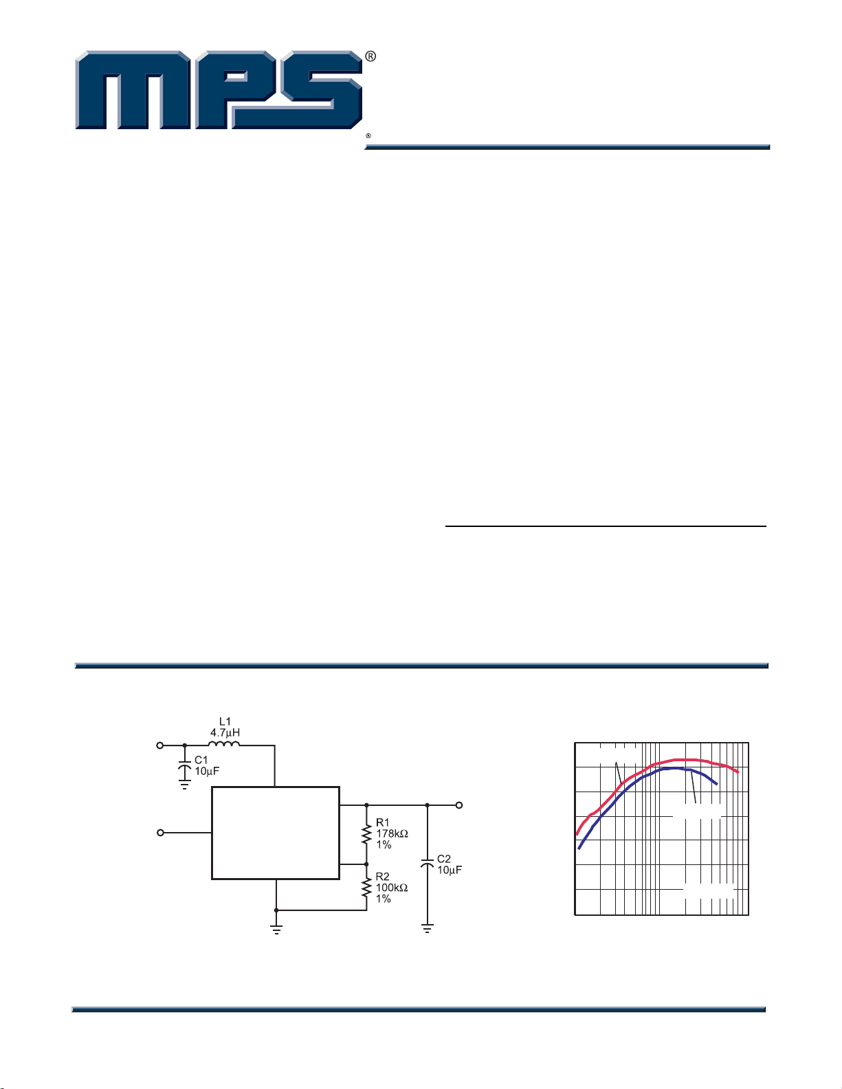
TYPICAL APPLICATION
V
IN
1.8V - 3.2V
4
SW
EN
5
EN
MP3410
GND
2
OUT
FB
Efficiency vs
Load Current
100
3
1
V
OUT
3.3V
400mA
EFFICIENCY (%)
VIN=3.6V
90
80
70
60
50
40
30
10 100 1000
LOAD CURRENT (mA)
VIN=2.4V
V
OUT
=5V
MP3410 Rev. 1.12 www.MonolithicPower.com 1
6/30/2011 MPS Proprietary Information. Patent Protected. Unauthorized Photocopy and Duplication Prohibited.
© 2011 MPS. All Rights Reserved.
Page 2
MP3410 — 1.3A, 550kHz SYNCHRONOUS RECTIFIED STEP-UP CONVERTER
ORDERING INFORMATION
Part Number* Package Top Marking Free Air Temperature (TA)
MP3410DJ
TSOT23-5
P3
-40°C to +85°C
* For Tape & Reel, add suffix –Z (e.g. MP3410DJ–Z)
For RoHS compliant packaging, add suffix –LF (e.g. MP3410DJ–LF–Z)
PACKAGE REFERENCE
TOP VIEW
FB
GND
OUT
1
2
3
TSOT23-5
54EN
SW
ABSOLUTE MAXIMUM RATINGS
(1)
All Pins.........................................-0.3V to +6.5V
Continuous Power Dissipation (T
= +25°C)
A
(2)
........................................................... 0.47W
Storage Temperature............... -65°C to +150°C
Recommended Operating Conditions
(3)
Supply Voltage VIN.............................1.8V to 6V
Output Voltage V
Maximum Junction Temp. (T
...........................2.5V to 6V
OUT
) .............. +125°C
J
Thermal Resistance
(4)
θ
JA
θJC
TSOT23-5.............................. 220.... 110.. °C/W
Notes:
1) Exceeding these ratings may damage the device.
2) The maximum allowable power dissipation is a function of the
maximum junction temperature T
ambient thermal resistance
. The maximum allowable continuous power dissipation at
T
A
any ambient temperature is calculated by P
)/JA. Exceeding the maximum allowable power dissipation
T
A
will cause excessive die temperature, and the regulator will go
into thermal shutdown. Internal thermal shutdown circuitry
protects the device from permanent damage.
3) The device is not guaranteed to function outside of its
operating conditions.
4) Measured on JESD51-7 4-layer board.
(MAX), the junction-to-
J
, and the ambient temperature
JA
(MAX)=(TJ(MAX)-
D
MP3410 Rev. 1.12 www.MonolithicPower.com 2
6/30/2011 MPS Proprietary Information. Patent Protected. Unauthorized Photocopy and Duplication Prohibited.
© 2011 MPS. All Rights Reserved.
Page 3
MP3410 — 1.3A, 550kHz SYNCHRONOUS RECTIFIED STEP-UP CONVERTER
ELECTRICAL CHARACTERISTICS
VEN = V
Parameter Symbol Condition Min Typ Max Units
Startup Supply Voltage VST
Output Voltage Range V
Supply Current (Shutdown) VEN = V
Supply Current VFB = 1.3V 360 A
Feedback Voltage VFB 1.15 1.19 1.23 V
Feedback Input Current VFB = 1.19V 50 nA
Switching Frequency fSW 410 550 690 KHz
Maximum Duty Cycle D
EN Input Low Voltage 0.4 V
EN Input High Voltage
(see Chart EN high voltage vs
Input for details)
EN Pull Down Resistor 1 m
Low-Side On Resistance
Low-Side Current Limit I
High-Side On Resistance
Thermal Shutdown
Thermal Shutdown Hysteresis
Note:
5) Guaranteed by design, not tested.
= 3.3V, TA = +25°C, unless otherwise noted.
OUT
I
= 0mA 1.5 1.6 1.8
LOAD
R
= 50 1.65
LOAD
2.5 6.0 V
OUT
OUT
80 90 95 %
MAX
V
=1.8V
IN
VIN =3.3V 1.65
V
(5)
R
(5)
R
(5)
160
ONLS
1.3 A
LIM
ONHS
(5)
30
=5V 2.15
IN
V
V
= 3.3V 300 m
OUT
= 3.3V 530 700 m
OUT
V
=0V, VSW = 5V 0.15 0.5 A
1.05
V
°C
°C
MP3410 Rev. 1.12 www.MonolithicPower.com 3
6/30/2011 MPS Proprietary Information. Patent Protected. Unauthorized Photocopy and Duplication Prohibited.
© 2011 MPS. All Rights Reserved.
Page 4

MP3410 — 1.3A, 550kHz SYNCHRONOUS RECTIFIED STEP-UP CONVERTER
TYPICAL PERFORMANCE CHARACTERISTICS
Circuit on front page, VIN = 2.4V, V
= 3.3V, TA = +25°C, unless otherwise noted.
OUT
MP3410 Rev. 1.12 www.MonolithicPower.com 4
6/30/2011 MPS Proprietary Information. Patent Protected. Unauthorized Photocopy and Duplication Prohibited.
© 2011 MPS. All Rights Reserved.
Page 5

MP3410 — 1.3A, 550kHz SYNCHRONOUS RECTIFIED STEP-UP CONVERTER
TYPICAL PERFORMANCE CHARACTERISTICS (continued)
Circuit on front page, V
= 2.4V, V
IN
= 3.3V, TA = +25°C, unless otherwise noted.
OUT
PIN FUNCTIONS
Pin # Name Description
1 FB
2 GND Ground.
3 OUT Supply Input for the MP3410. Connect to the output of the converter.
4 SW
5 EN
MP3410 Rev. 1.12 www.MonolithicPower.com 5
6/30/2011 MPS Proprietary Information. Patent Protected. Unauthorized Photocopy and Duplication Prohibited.
© 2011 MPS. All Rights Reserved.
Regulation Feedback Input. Connect to an external resistive voltage divider from the output to
FB to set the output voltage.
Output Switching Node. SW is the drain of the internal low-side N-Channel MOSFET and
high-side P-Channel MOSFET. Connect the inductor to SW to complete the step-up converter.
Regulator On/Off Control Input. A logic high input turns on the regulator. A logic low input (V
EN
< 0.4V) puts the MP3410 into low current shutdown mode. EN Input High Voltage will shift
upward for a higher V
. For a given VIN, as long as the voltage applied at EN pin is equal to or
IN
higher than correspondent EN-High-min value specified in the EC table , the part can turn on
normally.
Page 6

OPERATION
MP3410 — 1.3A, 550kHz SYNCHRONOUS RECTIFIED STEP-UP CONVERTER
REFERENCE VOLTAGE
THERMAL SHUTDOWN
OSC
500KHz
RAMP
+
UVLO
BIAS CURRENT
PWM
COMPARATOR
CONTROL
LOGIC
Figure 1—Functional Block Diagram
The MP3410 uses a 550kHz fixed-frequency,
current-mode regulation architecture to regulate
the output voltage. The MP3410 measures the
output voltage through an external resistive
voltage divider and compares that to the
internal 1.2V reference to generate the error
voltage. The current-mode regulator compares
the error voltage to the inductor current to
regulate the output voltage. The use of
current-mode regulation improves transient
response and control loop stability.
When the MP3410 is disabled (EN = Low), both
power switches are off. The body of the
P-Channel MOSFET connects to SW and there
is no current path from SW to OUT. Therefore,
the output voltage discharges to ground. When
the MP3410 is enabled (EN = High), the body of
the P-Channel MOSFET connects to OUT and
forms a forward diode from SW to OUT. Thus
the output voltage rises up toward the input
voltage. When output voltage crosses 1.6V the
MP3410 starts the controller and regulates the
output voltage to the target value.
EN
OUT
SW
CURRENT
SENSE
AMPLIFIER
ERROR
AMPLIFIER
RS
GND
FB
1.2V
At the beginning of each cycle, the N-Channel
MOSFET switch is turned on, forcing the
inductor current to rise. The current at the
source of the switch is internally measured and
converted to a voltage by the current sense
amplifier. That voltage is compared to the error
voltage. When the inductor current rises
sufficiently, the PWM comparator turns off the
switch, forcing the inductor current to the output
capacitor through the internal P-Channel
MOSFET rectifier, which forces the inductor
current to decrease. The peak inductor current
is controlled by the error voltage, which in turn
is controlled by the output voltage. Thus the
output voltage controls the inductor current to
satisfy the load.
Soft-Start
The MP3410 includes a soft-start timer that
limits the voltage at the error amplifier output
during startup to prevent excessive current at
the input. This prevents premature termination
of the source voltage at startup due to inrush
current. This also limits the inductor current at
startup, forcing the input current to rise slowly to
the amount required to regulate the output
voltage during soft-start.
MP3410 Rev. 1.12 www.MonolithicPower.com 6
6/30/2011 MPS Proprietary Information. Patent Protected. Unauthorized Photocopy and Duplication Prohibited.
© 2011 MPS. All Rights Reserved.
Page 7

MP3410 — 1.3A, 550kHz SYNCHRONOUS RECTIFIED STEP-UP CONVERTER
(
)
×
(
=
Δ
APPLICATION INFORMATION
COMPONENT SELECTION
Selecting the Inductor
Setting the Output Voltage
Set the output voltage by selecting the resistive
voltage divider ratio. The voltage divider drops
the output voltage to the 1.19V feedback
voltage. Use a 100k resistor for R2 of the
voltage divider. Determine the high-side resistor
R1 by the equation:
−
VV
FBOUT
⎞
⎟
⎟
2R
⎠
Where V
=
1R
is the output voltage, VFB is the
OUT
V
⎛
FB
⎜
⎜
⎝
1.19V feedback voltage and R2=100k.
Selecting the Input Capacitor
An input capacitor is required to supply the AC
ripple current to the inductor, while limiting noise
at the input source. Multi-layer ceramic
capacitors are the best choice as they have
extremely low ESR and are available in small
footprints. Use an input capacitor value of 4.7F
or greater. This capacitor must be placed
physically close to the device.
Selecting the Output Capacitor
A single 4.7µF to 10µF ceramic capacitor
usually provides sufficient output capacitance
for most applications. Larger values up to 22µF
may be used to obtain extremely low output
voltage ripple and improve transient response.
The impedance of the ceramic capacitor at the
switching frequency is dominated by the
capacitance, and so the output voltage ripple is
mostly independent of the ESR. The output
voltage ripple V
is calculated as:
RIPPLE
The inductor is required to force the output
voltage higher while being driven by the lower
input voltage. A good rule for determining the
inductance is to allow the peak-to-peak ripple
current to be approximately 30%-50% of the
maximum input current. Make sure that the
peak inductor current is below the minimum
current limit at the duty cycle used (to prevent
loss of regulation due to the current limit
variations).
Calculate the required inductance value L using
the equations:
) V- (VV
INOUTIN
IfV
Δ××
SWOUT
×
IV
LOADOUT
V
IN
)
I%50%30I −
)MAX(
η×
)MAX(IN
Where I
I
LOAD(MAX)
L
=
=
)MAX(IN
is the maximum load current, I
is the peak-to-peak inductor ripple current and
is efficiency. For the MP3410, typically, 4.7µH is
recommended for most applications. Choose an
inductor that does not saturate at the peak
switch current as calculated above with
additional margin to cover heavy load transients
and extreme startup conditions.
VVI
−
UT
××
IN
f2CV
SW
LOAD
is the load
Where V
V
RIPPLE
is the input voltage, I
IN
=
OLOAD
O
UT
current, C2 is the capacitance of the output
capacitor and f
is the 550kHz switching
SW
frequency.
MP3410 Rev. 1.12 www.MonolithicPower.com 7
6/30/2011 MPS Proprietary Information. Patent Protected. Unauthorized Photocopy and Duplication Prohibited.
© 2011 MPS. All Rights Reserved.
Page 8

MP3410 — 1.3A, 550kHz SYNCHRONOUS RECTIFIED STEP-UP CONVERTER
Selecting the Feed-Forward Capacitor
A feed-forward capacitor C3 in parallel with the
high-side resistor R1 can be added to improve
the output ripple at discontinuous conduction
mode and the load transient response (see
Figure 2). Up to 220pF for this capacitor is
recommended for 3.3V output applications.
Selecting the Schottky Diode
A Schottky diode D1 in parallel with the highside P-Channel MOSFET is necessary to clamp
the SW node to a safe level for outputs of 4V or
above. A 0.5A, 20V Schottky diode can be used
for this purpose. See Figure 3.
V
IN
1.8V - 3.2V
4
EN
SW
5
EN
MP3410
OUT
LAYOUT CONSIDERATIONS
High frequency switching regulators require
very careful layout for stable operation and low
noise. All components must be placed as close
to the IC as possible. All feedback components
must be kept close to the FB pin to prevent
noise injection on the FB pin trace. The ground
return of C1 and C2 should be tied close to the
GND pin. See the MP3410 demo board layout
for reference.
3
C3
Up to 220pF
OPTIONAL
V
OUT
3.3V
400mA
1
GND
FB
2
Figure 2—3.3V Typical Application Circuit with Feed-Forward Capacitor
4
SW
5
EN
MP3410
GND
2
OUT
FB
3
1
Figure 3—5V Typical Application Circuit with External Schottky Diode and Output Disconnect
Not Required
MP3410 Rev. 1.12 www.MonolithicPower.com 8
6/30/2011 MPS Proprietary Information. Patent Protected. Unauthorized Photocopy and Duplication Prohibited.
© 2011 MPS. All Rights Reserved.
Page 9

MP3410 — 1.3A, 550kHz SYNCHRONOUS RECTIFIED STEP-UP CONVERTER
D1
V
IN
2.5V - 4.2V
P1
V
OUT
5V
400mA
EN
4
SW
5
EN
MP3410
GND
2
OUT
FB
3
1
Figure 4—5V Typical Application Circuit with External Schottky Diode and Output Disconnect
Required
V
2.5V-4.2V
EN
Vin
3V
EN
L1
C3
470pF
IN
4
SW
OUT
3
V
OUT
5V
5
EN
MP3410
GND
FB
1
400mA
2
Figure 5—5V Typical Application Circuit
10
C1
L1
4.7
4
SW
MP3410
5
EN
GND
2
OUT
FB
B130
3
R1
220 k
1
R2
100 k
Vout
3.8 V
750 m A
C2
10
Figure 6—3V-3.8V/750mA Application
MP3410 Rev. 1.12 www.MonolithicPower.com 9
6/30/2011 MPS Proprietary Information. Patent Protected. Unauthorized Photocopy and Duplication Prohibited.
© 2011 MPS. All Rights Reserved.
Page 10

MP3410 — 1.3A, 550kHz SYNCHRONOUS RECTIFIED STEP-UP CONVERTER
PACKAGE INFORMATION
2.80
3.00
45
TSOT23-5
1.20
TYP
0.60
TYP
0.95
BSC
0.84
0.90
0.30
0.50
1
TOP VIEW
0.95 BSC
1.50
1.70
3
1.00 MAX
0.00
0.10
2.60
3.00
RECOMMENDED LAND PATTERN
SEATING PLANE
SEE DETAIL "A"
FRONT VIEW SIDE VIEW
2.60
TYP
0.09
0.20
NOTE:
GAUGE PLANE
0.25 BSC
o
0o-8
DETAIL A
0.30
0.50
1) ALL DIMENSIONS ARE IN MILLIMETERS.
2) PACKAGE LENGTH DOES NOT INCLUDE MOLD FLASH,
PROTRUSION OR GATE BURR.
3) PACKAGE WIDTH DOES NOT INCLUDE INTERLEAD FLASH
OR PROTRUSION.
4) LEAD COPLANARITY (BOTTOM OF LEADS AFTER FORMING)
SHALL BE 0.10 MILLIMETERS MAX.
5) DRAWING CONFORMS TO JEDEC MO-193, VARIATION AA.
6) DRAWING IS NOT TO SCALE.
NOTICE: The information in this document is subject to change without notice. Users should warrant and guarantee that third
party Intellectual Property rights are not infringed upon when integrating MPS products into any application. MPS will not
assume any legal responsibility for any said applications.
MP3410 Rev. 1.12 www.MonolithicPower.com 10
6/30/2011 MPS Proprietary Information. Patent Protected. Unauthorized Photocopy and Duplication Prohibited.
© 2011 MPS. All Rights Reserved.
 Loading...