

MMBFJ270
P-Channel Switch
Features
• This device is designed for low level analog switching sample and hold
circuits and chopper stabilized amplifiers.
• Sourced from process 88.
Absolute Maximum Ratings (Note1) T
= 25°C unless otherwise n oted
a
Symbol Parameter Value Units
G
D
SOT-23
Mark : 61S
MMBFJ270 — P-Channel Switch
August 2008
S
V
DG
V
GS
I
GF
TJ, T
STG
Note1 : These ratings are limiting values above which the serviceability of any semiconductor device may by impaired.
These are steady state limits. The factory should be consulted on applications involving pulsed or low duty cycle operations
Drain-Gate Voltage -30 V
Gate-Source Voltage 30 V
Forward Gate Current 50 mA
Operating and Storage Junction Temperature Range -55 ~ 150 °C
Thermal Characteristics
Symbol Parameter Value Units
P
D
R
θJA
Note2 : Device mounted on FR-4 PCB, 1 inch x 0.85 inch x 0.062 inch
Electrical Characteristics T
Symbol Parameter Test Condition MIN MAX Units
Off Characteristics (Note3)
V
(BR)GSS
I
GSS
V
GS(off)
On Characteristics (Note3)
Total Device Dissipation
Derate above 25°C
Thermal Resistance, Junction to Ambient (Note2) 556 °C/W
= 25°C unless otherwise noted
C
Gate-Source Breakdwon Voltage IG = 1.0µA, VDS = 0 30 V
Gate Reverse Current V
Gate-Source Cutoff Voltage V
= 20V, V
GS
= -15V, ID = -1.0nA 0.5 2.0 V
DS
= 0 200 pA
DS
225
1.8
mW
mW/°C
I
DSS
gfs Forward Transferconductance VGS = 0V, VDS = 15V, f = 1.0kHz 6000 15000 µmhos
goss Common- Source Output Conduc-
Note3 : Short duration test pulse used to minimize self-heating effect.
© 2008 Fairchild Semiconductor Corporation www.fairchildsemi.com
MMBFJ270 Rev. B 1
Zero-Gate Voltage Drain Current * VDS = -15V, VGS = 0 -2.0 -15 mA
V
= 0V, VDS = 15V, f = 1.0kHz 200 µmhos
tance
GS
Typical Characteristics
MMBFJ270 — P-Channel Switch
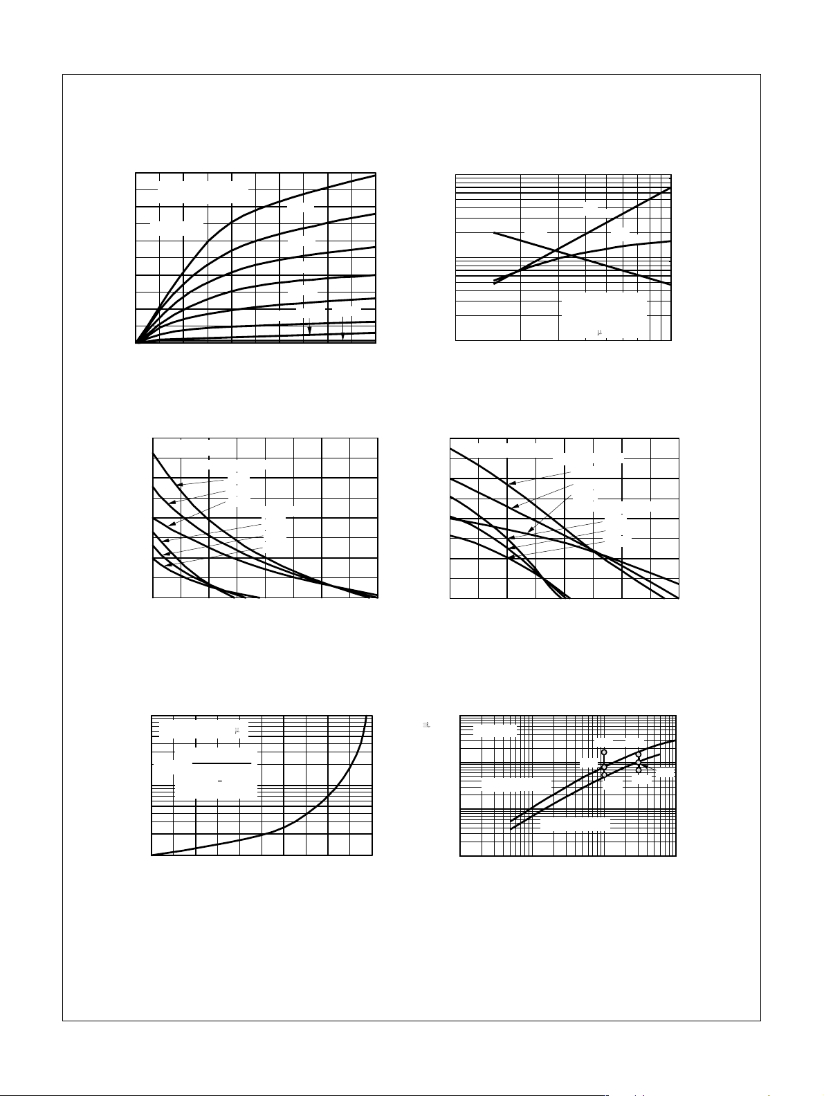
Common Drain-Source
-20
-16
-12
-8
-4
D
I - DRAIN CURRENT (mA)
0
T = 25°C
A
TYP V = 4.5 V
GS(off)
V = 0 V
GS
V - DRAIN-SOURCE VOLTAGE (V)
DS
0.5 V
1.0 V
1.5 V
2.0 V
2.5 V
3.0 V
3.5 V
Transfer Characteristics
-32
V = - 15 V
DS
-24
-16
-8
D
I - DRAIN CURRENT (mA)
0
01234
V = - 4.5 V
GS(off)
- 55°C
25°C
125°C
V = 2.5 V
GS(off)
- 55°C
25°C
125°C
V - GATE-SOURCE VOLTAGE (V)
GS
Parameter Interactions
100
50
r
DS
10
5
fs
1
g - TRANSCONDUCTANCE (mmhos)
-5-4-3-2-10
12 510
V - GATE CUTOFF VOLTAGE (V)
GS (OFF)
I
DSS
g
fs
fs
I , g @ V = 15V,
DSS
V = 0 PULSED
GS
r @ -100 mV, V = 0
DS
V @ V = - 15V,
GS(off)
I = - 1.0
D
DS
GS
DS
DS
A
1,000
500
100
50
10
r - DRAIN "ON" RESISTANCE
DS
(
Ω
)
Transfer Characteristics
16
12
D
I - DRAIN CURRENT (mA)
V = - 15 V
DS
8
V = - 4.5 V
GS(off)
- 55°C
25°C
125°C
V = 2.5 V
GS(off)
- 55°C
125°C
25°C
4
0
01234
V - GATE-SOURCE VOLTAGE (V)
GS
Normalized Drain Resistance
Ω ) Ω )
Ω ) Ω )
Ω )
(
100
50
20
10
5
2
DS
1
r - NORMALIZED RESISTANCE
0 0.2 0.4 0.6 0.8 1
V /V - NORMALIZED GATE-SOURCE VOLTAGE (V)
GS
vs Bias Voltage
V @ 5.0V, 10 A
GS(off)
r
________
1 -
V
DS
GS
V
GS(off)
r =
DS
GS(off)
os
g - OUTPUT CONDUCTANCE ( mhos)
1000
100
Output Conductance
vs Drain Current
f = 1.0 kHz
V = - 4.5V
GS(off)
10
V = - 2.5V
GS(off)
1
_
0.01 0.1 1 10
_
I - DRAIN CURRENT (mA)
D
-10V
-5.0V
_
-20V
-5.0V
-20V
-10V
_
© 2008 Fairchild Semiconductor Corporation www.fairchildsemi.com
MMBFJ270 Rev. B 2

Typical Characteristics (Continued)
MMBFJ270 — P-Channel Switch
Transconductance
vs Drain Current
10
V = 2.5V
GS(off)
5
1
25°C
V = 6.0V
GS(off)
- 55°C
25°C
125°C
0.5
V = -15V
DG
f = 1.0 kHz
0.1
_
fs
0.1 1 10 100
g - TRANSCONDUCTANCE (mmhos)
_
I - DRAIN CURRENT (mA)
D
_
Noise Voltage vs Frequency
100
√
50
I = - 0.2 mA
D
I = 5.0 mA
10
n
e - NOISE VOLTAGE (nV / Hz)
D
5
V = - 15V
DG
BW = 6.0 Hz @ f = 10 Hz, 100 Hz
= 0.2f @ f ≥ 1.0 kHz
1
0.01 0.1 1 10 100
f - FREQUENCY (kHz)
Capacitance vs Voltage
100
f = 0.1 - 1.0 MHz
C (V = -15V)
DS
10
5
rs
is
C (C ) - CAPACITANCE (pF)
_
1
048121620
V - GATE-SOURCE VOLTAGE (V)
GS
is
C (V = -15V)
DS
rs
Channel Resistance
)
Ω
(
1000
DS
r - DRAIN "ON" RESISTANCE
500
100
50
10
vs Temperat ure
V = -100 mV
V = 2.5V
GS(off)
V = 4.5V
GS(off)
V = 8.0V
GS(off)
-50 0 50 100 150
T - AMBIENT TEMPERATURE ( C)
A
DS
V = 0
GS
o
Power Derating
300
250
200
150
100
[W], POWER DISSIPATION
C
50
P
0
0 25 50 75 100 125 150 175
Tc[oC], CASE TEMPERATURE
© 2008 Fairchild Semiconductor Corporation www.fairchildsemi.com
MMBFJ270 Rev. B 3

Package Dimensions
0
F
3
N
MMBFJ270 — P-Channel Switch
SOT-23
0.40 ±0.03
2.90 ±0.10
0.95 ±0.03 0.95 ±0.03
0.20 MI
0.45~0.60
±0.10
0.03~0.1
2.40
0.38 RE
0.40 ±0.03
0.12
+0.05
–0.02
0.96~1.14
0.97REF 1.30 ±0.10
1.90 ±0.03
0.508REF
Dimensions in Millimeters
© 2008 Fairchild Semiconductor Corporation www.fairchildsemi.com
MMBFJ270 Rev. B 4

MMBFJ270 P-Channel SwitchMMBFJ270
© 2008 Fairchild Semiconductor Corporation www.fairchildsemi.com
MMBFJ270 Rev. B 5
 Loading...