

Page 1
SEMICONDUCTOR TECHNICAL DATA
N–Channel
3
GATE
2 SOURCE
Order this document
by MMBF5484LT1/D
Motorola Preferred Device
MAXIMUM RATINGS
Rating Symbol Value Unit
Drain–Gate Voltage V
Reverse Gate–Source Voltage V
Forward Gate Current I
Continuous Device Dissipation at or Below
TC = 25°C
Linear Derating Factor
Storage Channel Temperature Range T
THERMAL CHARACTERISTICS
Characteristic Symbol Max Unit
Total Device Dissipation FR–5 Board
TA = 25°C
Derate above 25°C
Thermal Resistance, Junction to Ambient
Junction and Storage Temperature TJ, T
(1)
DEVICE MARKING
MMBF5484LT1 = 6B
ELECTRICAL CHARACTERISTICS (T
Characteristic Symbol Min Max Unit
= 25°C unless otherwise noted)
A
OFF CHARACTERISTICS
Gate–Source Breakdown Voltage
(IG = –1.0 µAdc, VDS = 0)
Gate Reverse Current
(VGS = –20 Vdc, VDS = 0)
(VGS = –20 Vdc, VDS = 0, TA = 100°C)
Gate Source Cutoff Voltage
(VDS = 15 Vdc, ID = 10 nAdc)
ON CHARACTERISTICS
Zero–Gate–Voltage Drain Current
(VDS = 15 Vdc, VGS = 0)
SMALL–SIGNAL CHARACTERISTICS
Forward Transfer Admittance
(VDS = 15 Vdc, VGS = 0, f = 1.0 kHz)
Output Admittance
(VDS = 15 Vdc, VGS = 0, f = 1.0 kHz)
1. FR–5 = 1.0 0.75 0.062 in.
DG
GS(r)
G(f)
P
stg
P
R
q
D
D
JA
stg
1 DRAIN
25 Vdc
25 Vdc
10 mAdc
200
2.8
–65 to +150 °C
225
1.8
556 °C/W
–55 to +150 °C
mW
mW/°C
mW
mW/°C
V
3
1
2
CASE 318–08, STYLE 10
SOT–23 (TO–236AB)
(BR)GSS
I
GSS
V
GS(off)
I
DSS
|Yfs| 3000 6000 µmhos
|yos| — 50 µmhos
–25 — Vdc
—
—
–0.3 –3.0 Vdc
1.0 5.0 mAdc
–1.0
–0.2
nAdc
µAdc
Thermal Clad is a trademark of the Bergquist Company
Preferred devices are Motorola recommended choices for future use and best overall value.
Motorola Small–Signal Transistors, FETs and Diodes Device Data
Motorola, Inc. 1996
1
Page 2
MMBF5484LT1
ELECTRICAL CHARACTERISTICS
(TA = 25°C unless otherwise noted) (Continued)
Characteristic Symbol Min Max Unit
SMALL–SIGNAL CHARACTERISTICS (Continued)
Input Capacitance
(VDS = 15 Vdc, VGS = 0, f = 1.0 MHz)
Reverse Transfer Capacitance
(VDS = 15 Vdc, VGS = 0, f = 10 MHz)
Output Capacitance
(VDS = 15 Vdc, VGS = 0, f = 1.0 MHz)
FUNCTIONAL CHARACTERISTICS
Noise Figure
(VDS = 15 Vdc, ID = 1.0 mAdc, YG′ = 1.0 mmhos)
(RG = 1.0 kΩ, f = 100 MHz)
(VDS = 15 Vdc, VGS = 0, YG′ = 1.0 µmhos)
(RG = 1.0 MΩ, f = 1.0 kHz)
Common Source Power Gain
(VDS = 15 Vdc, ID = 1.0 mAdc, f = 100 MHz)
POWER GAIN
C
iss
C
rss
C
oss
NF
G
ps
— 5.0 pF
— 1.0 pF
— 2.0 pF
dB
—
—
16 25 dB
3.0
2.5
24
20
16
12
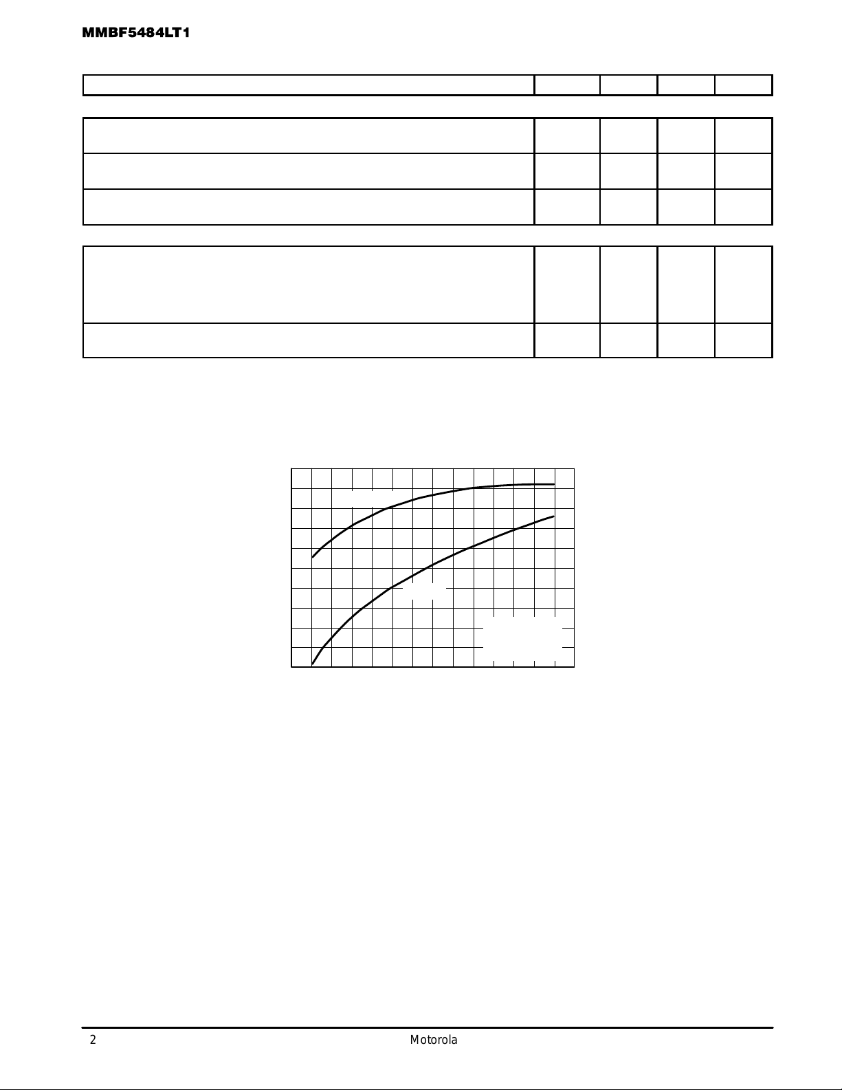
, POWER GAIN (dB)
G
P
8.0
4.0
0 4.0 6.0 8.0 10 12 14
f = 100 MHz
2.0
400 MHz
T
channel
VDS = 15 Vdc
VGS = 0 V
ID, DRAIN CURRENT (mA)
= 25°C
Figure 1. Effects of Drain Current
2
Motorola Small–Signal Transistors, FETs and Diodes Device Data
Page 3
MMBF5484LT1
NEUTRALIZING
COIL
INPUT
TO 50
SOURCE
*L1 17 turns, (approx. — depends upon circuit layout) AWG #28
enameled copper wire, close wound on 9/32″ ceramic coil
form. Tuning provided by a powdered iron slug.
*L2 4–1/2 turns, AWG #18 enameled copper wire, 5/16″ long,
3/8″ I.D. (AIR CORE).
*L3 3–1/2 turns, AWG #18 enameled copper wire, 1/4″ long,
3/8″ I.D. (AIR CORE).
C1
Ω
Adjust VGS for
ID = 50 mA
VGS < 0 Volts
′
g
L1
C5
L3R
C6
C2
CASE
V
NOTE: The noise source is a hot–cold body
COMMON
GS
V
+15 V
(AIL type 70 or equivalent) with a
test receiver (AIL type 136 or equivalent).
Figure 2. 100 MHz and 400 MHz Neutralized Test Circuit
10
ID = 5.0 mA
8.0
C4
L2
C7
DS
ID = 5.0 mA
NOISE FIGURE
(T
channel
C3
= 25°C)
Reference
Designation
C1
TO 500
Ω
LOAD
**L1 6 turns, (approx. — depends upon circuit layout) AWG #24
enameled copper wire, close wound on 7/32″ ceramic coil
form. Tuning provided by an aluminum slug.
**L2 1 turn, AWG #16 enameled copper wire, 3/8″ I.D.
(AIR CORE).
**L3 1/2 turn, AWG #16 enameled copper wire, 1/4″ I.D.
(AIR CORE).
C2 1000 pF 17 pF
C3 3.0 pF 1.0 pF
C4 1–12 pF 0.8–8.0 pF
C5 1–12 pF 0.8–8.0 pF
C6 0.0015 µF 0.001 µF
C7 0.0015 µF 0.001 µF
L1 3.0 µH* 0.2 µH**
L2 0.15 µH* 0.03 µH**
L3 0.14 µH* 0.022 µH**
VALUE
100 MHz 400 MHz
7.0 pF 1.8 pF
6.5
5.5
VDS = 15 V
VGS = 0 V
6.0
f = 400 MHz
4.0
NF, NOISE FIGURE (dB)
2.0
100 MHz
0
0 4.0 6.0 8.0 10 12 14
2.0
VDS, DRAIN–SOURCE VOLTAGE (VOLTS)
Figure 3. Effects of Drain–Source Voltage Figure 4. Effects of Drain Current
4.5
3.5
NF, NOISE FIGURE (dB)
16 18 20
2.5
1.5
0 4.0 6.0 8.0 10 12 14
100 MHz
2.0
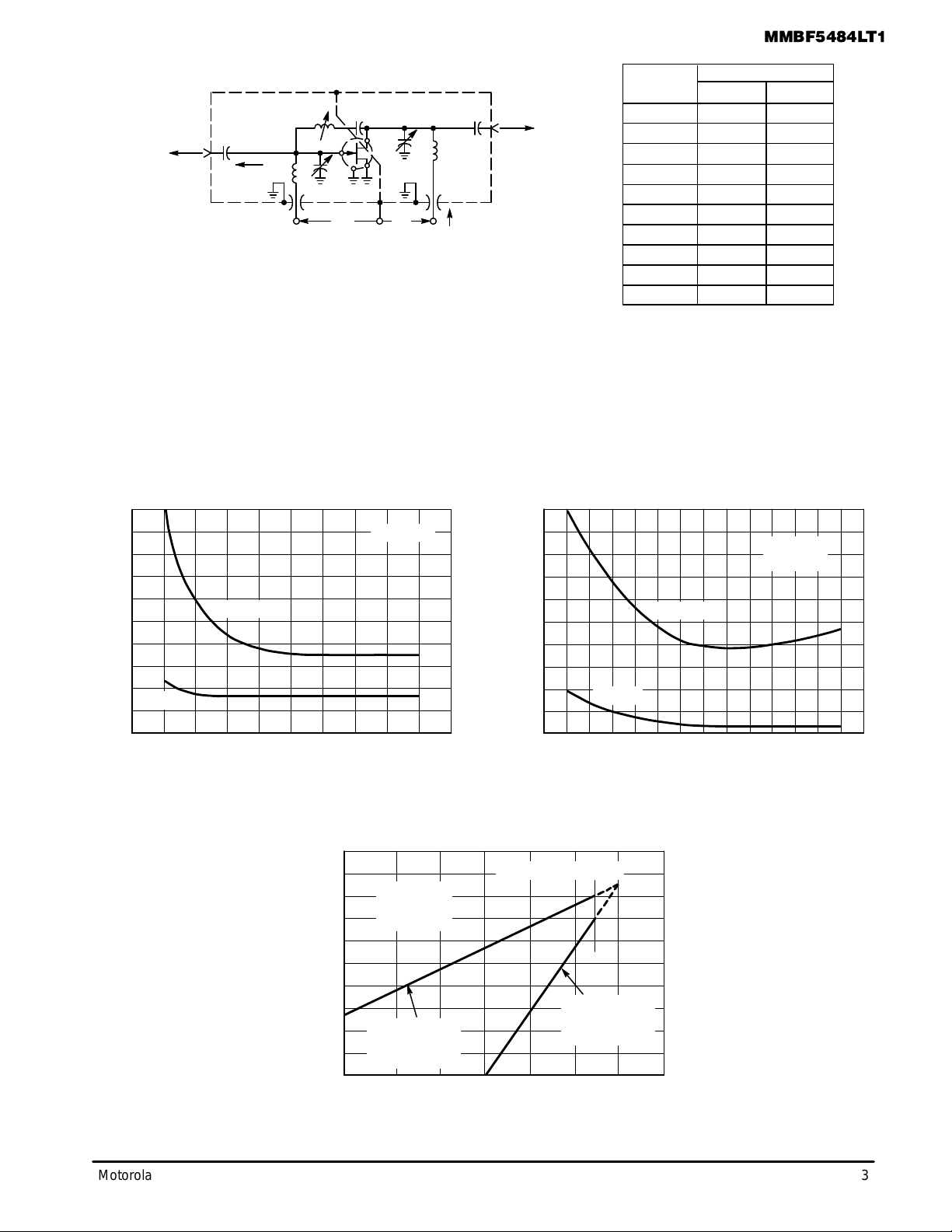
INTERMODULA TION CHARACTERISTICS
+40
+20
VDS = 15 Vdc
0
–20
f1 = 399 MHz
f2 = 400 MHz
–40
–60
–80
–100
–120
out
P , OUTPUT POWER PER TONE (dB)
–140
–160
FUNDAMENT AL
OUTPUT @ I
0.25 I
DSS
DSS
–120 –100 –80 –60 –40 –20 0 +20
Pin, INPUT POWER PER TONE (dB)
3RD ORDER INTERCEPT
,
3RD ORDER IMD
OUTPUT @ I
0.25 I
DSS
f = 400 MHz
ID, DRAIN CURRENT (mA)
,
DSS
Figure 5. Third Order Intermodulation Distortion
Motorola Small–Signal Transistors, FETs and Diodes Device Data
3
Page 4

MMBF5484LT1
COMMON SOURCE CHARACTERISTICS
ADMITTANCE PARAMETERS
(VDS = 15 Vdc, T
channel
= 25°C)
30
20
10
7.0
5.0
3.0
2.0
1.0
, INPUT SUSCEPT ANCE (mmhos)
, INPUT CONDUCT ANCE (mmhos)
is
0.7
is
b
g
0.5
0.3
10
bis @ 0.25 I
20 30 50 70 100 200 300
DSS
f, FREQUENCY (MHz)
Figure 6. Input Admittance (yis) Figure 7. Reverse Transfer Admittance (yrs)
20
10
7.0
5.0
3.0
2.0
1.0
0.7
0.5
|, FORWARD SUSCEPTANCE (mmhos)
fs
|b
0.3
, FORWARD TRANSCONDUCTANCE (mmhos)
fs
g
0.2
10 20 30 50 70 100 200 300
|bfs| @ I
gfs @ 0.25 I
DSS
f, FREQUENCY (MHz)
bis @ I
DSS
gis @ I
gis @ 0.25 I
gfs @ I
DSS
|bfs| @ 0.25 I
DSS
DSS
DSS
DSS
500 700
500 700
1000
1000
5.0
3.0
2.0
1.0
0.7
0.5
0.3
0.2
, REVERSE SUSCEPTANCE (mmhos)
0.1
rs
, REVERSE TRANSADMITTANCE (mmhos)
b
rs
0.07
g
0.05
10 20 30 50 70 100 200 300
f, FREQUENCY (MHz)
10
5.0
2.0
1.0
0.5
0.2
0.1
, OUTPUT ADMITTANCE (mhos)
0.05
, OUTPUT SUSCEPT ANCE (mhos)
os
os
g
b
0.02
0.01
10 20 30 50 70 100 200 300
bos @ I
and 0.25 I
DSS
f, FREQUENCY (MHz)
brs @ I
grs @ I
DSS
DSS
0.25 I
, 0.25 I
DSS
gos @ I
gos @ 0.25 I
DSS
DSS
DSS
500 700
500 700
1000
DSS
1000
Figure 8. Forward Transadmittance (yfs) Figure 9. Output Admittance (yos)
4
Motorola Small–Signal Transistors, FETs and Diodes Device Data
Page 5

COMMON SOURCE CHARACTERISTICS
S–P ARAMETERS
(VDS = 15 Vdc, T
channel
= 25°C, Data Points in MHz)
MMBF5484LT1
100
110
120
130
140
°
DSS
800
200
°
500
700
°
0.4
0.3
900
0.2
0.1
0.0
100
180°190°200°210
170
°
20
30
ID = I
150
°
DSS
°
, 0.25 I
600
400
300
160
0°350°340°330
10
20
30
°
40
°
50
°
60
°
70
°
80
°
90
°
°
°
°
°
°
160
150
°
°
°
ID = 0.25 I
100
1.0
100
900
ID = I
800
200
DSS
700
0.9
0.8
0.7
0.6
180°190°200°210
170
°
°
200
300
600
400
500
900
300
DSS
400
800
°
700
°
500
600
320
310
300
290
280
270
260
250
240
230
220
40
50
60
70
80
90
100
110
120
130
140
°
°
°
°
°
°
°
°
°
°
°
°
°
°
°
°
°
°
°
°
°
°
0°350°340°330
10
°
320
°
310
°
300
°
290
°
280
°
270
°
260
°
250
°
240
°
230
°
220
°
°
100
110
120
130
Figure 10. S
10
°
ID = 0.25 I
500
300
200
100
°
DSS
100
20
30
°
40
°
50
°
60
°
700
600
500
ID = I
800
400
DSS
900
900
800
700
600
400
300
200
70
°
80
°
90
°
°
°
°
°
11s
0°350°340°330
0.6
0.5
0.4
0.3
0.3
0.4
0.5
0.6
°
320
°
310
°
300
°
290
°
280
°
270
°
260
250
240
230
100
°
°
110
°
120
°
130
30
°
40
°
50
°
60
°
70
°
80
°
90
°
°
°
°
°
20
°
Figure 11. S
0°350°340°330
10
°
100
1.0
100
200
0.9
ID = I
0.8
0.7
0.6
200
300
DSS
12s
300
400
500
400
600
700
800
ID = 0.25 I
500
600
700
900
800
900
°
DSS
320
310
300
290
280
270
260
250
240
230
°
°
°
°
°
°
°
°
°
°
220
140
°
150
180°190°200°210
170
160
°
°
°
Figure 12. S
21s
°
°
Motorola Small–Signal Transistors, FETs and Diodes Device Data
140
220
°
180°190°200°210
170
150
160
°
°
°
Figure 13. S
22s
°
°
5
Page 6

MMBF5484LT1
COMMON GATE CHARACTERISTICS
ADMITTANCE PARAMETERS
(VDG = 15 Vdc, T
channel
= 25°C)
20
10
7.0
5.0
3.0
2.0
1.0
0.7
, INPUT SUSCEPT ANCE (mmhos)
, INPUT CONDUCT ANCE (mmhos)
ig
ig
b
g
big @ I
0.5
0.3
0.2 0.005
10
DSS
20 30 50 70 100 200 300
grg @ 0.25 I
big @ 0.25 I
f, FREQUENCY (MHz)
gig @ I
DSS
DSS
DSS
500 700
1000
Figure 14. Input Admittance (yig) Figure 15. Reverse Transfer Admittance (yrg)
10
7.0
5.0
3.0
2.0
gfg @ I
DSS
gfg @ 0.25 I
DSS
0.5
0.3
0.2
0.1
0.07
0.05
0.03
0.02
, REVERSE SUSCEPTANCE (mmhos)
0.01
rg
, REVERSE TRANSADMITTANCE (mmhos)
b
rg
g
0.007
1.0
0.7
0.5
0.3
0.2
brg @ I
0.25 I
gig @ I
10 20 30 50 70 100 200 300
f, FREQUENCY (MHz)
bog @ I
DSS
, 0.25 I
DSS
DSS
, 0.25 I
DSS
DSS
DSS
500 700
1000
1.0
0.7
0.5
bfg @ I
0.3
, FORWARD SUSCEPTANCE (mmhos)
0.2
fg
b
, FORWARD TRANSCONDUCTANCE (mmhos)
fg
g
0.1
10 20 30 50 70 100 200 300
DSS
f, FREQUENCY (MHz) f, FREQUENCY (MHz)
Figure 16. Forward Transfer Admittance (yfg) Figure 17. Output Admittance (yog)
brg @ 0.25 I
DSS
500 700
1000
0.1
0.07
0.05
0.03
, OUTPUT ADMITTANCE (mmhos)
, OUTPUT SUSCEPT ANCE (mmhos)
og
og
g
0.02
b
0.01
gog @ I
DSS
gog @ 0.25 I
10 20 30 50 70 100 200 300
DSS
500 700
1000
6
Motorola Small–Signal Transistors, FETs and Diodes Device Data
Page 7

COMMON GATE CHARACTERISTICS
S–P ARAMETERS
(VDS = 15 Vdc, T
channel
= 25°C, Data Points in MHz)
MMBF5484LT1
40
50
60
70
80
90
100
110
120
130
140
0°350°340°330
10
20
30
°
°
°
°
°
°
°
°
°
°
°
°
160
150
°
°
°
0.7
100
200
200
ID = I
300
DSS
300
400
400
500
0.6
100
0.5
0.4
0.3
180°190°200°210
170
°
°
ID = 0.25 I
500
600
600
700
800
900
700
°
DSS
800
900
°
320
310
300
290
280
270
260
250
240
230
220
°
600
900
°
0.04
0.03
0.02
0.01
0.0
100
500
ID = 0.25 I
600
700
800
900
170
°
°
DSS
0.01
0.02
0.03
0.04
180°190°200°210
20
30
°
40
50
60
70
80
90
100
110
120
130
140
°
°
°
°
°
°
°
ID = I
150
DSS
700
800
160
°
°
°
°
°
°
°
°
°
°
°
°
°
°
°
°
0°350°340°330
10
°
320
°
310
°
300
°
290
°
280
°
270
°
260
°
250
°
240
°
230
°
220
°
°
40
50
60
70
80
90
100
110
120
130
Figure 18. S
10
20
30
°
°
°
°
°
°
°
°
°
°
°
°
°
11g
0°350°340°330
0.5
100
0.4
0.3
0.2
0.1
100
ID = 0.25 I
ID = I
DSS
900
DSS
°
900
320
310
300
290
280
270
260
250
240
230
30
°
40
50
60
70
80
90
100
110
120
130
°
°
°
°
°
°
°
°
°
°
°
°
°
°
°
°
°
°
°
°
Figure 19. S
20
°
12g
0°350°340°330
10
°
1.5
1.0
200
100
0.9
0.8
0.7
0.6
300
ID = I
400
500
600
800 900
, 0.25 I
DSS
700
DSS
°
320
°
310
°
300
°
290
°
280
°
270
°
260
°
250
°
240
°
230
°
220
140
°
150
180°190°200°210
170
160
°
°
°
Figure 20. S
21g
°
°
Motorola Small–Signal Transistors, FETs and Diodes Device Data
140
220
°
180°190°200°210
170
150
160
°
°
°
Figure 21. S
22g
°
°
7
Page 8

MMBF5484LT1
INFORMATION FOR USING THE SOT–23 SURFACE MOUNT PACKAGE
MINIMUM RECOMMENDED FOOTPRINT FOR SURFACE MOUNTED APPLICATIONS
Surface mount board layout is a critical portion of the total
design. The footprint for the semiconductor packages must
be the correct size to insure proper solder connection
0.037
0.95
0.035
0.9
SOT–23 POWER DISSIP ATION
The power dissipation of the SOT–23 is a function of the
pad size. This can vary from the minimum pad size for
soldering to a pad size given for maximum power dissipation.
Power dissipation for a surface mount device is determined
by T
die, R
ambient, and the operating temperature, TA. Using the
values provided on the data sheet for the SOT–23 package,
PD can be calculated as follows:
The values for the equation are found in the maximum
ratings table on the data sheet. Substituting these values into
the equation for an ambient temperature TA of 25°C, one can
calculate the power dissipation of the device which in this
case is 225 milliwatts.
The 556°C/W for the SOT–23 package assumes the use
of the recommended footprint on a glass epoxy printed circuit
board to achieve a power dissipation of 225 milliwatts. There
are other alternatives to achieving higher power dissipation
from the SOT–23 package. Another alternative would be to
use a ceramic substrate or an aluminum core board such as
Thermal Clad. Using a board material such as Thermal
Clad, an aluminum core board, the power dissipation can be
doubled using the same footprint.
, the maximum rated junction temperature of the
J(max)
, the thermal resistance from the device junction to
θJA
PD =
T
PD =
150°C – 25°C
556°C/W
J(max)
R
θJA
– T
A
= 225 milliwatts
0.031
0.8
SOT–23
interface between the board and the package. With the
correct pad geometry, the packages will self align when
subjected to a solder reflow process.
0.037
0.95
0.079
2.0
inches
mm
SOLDERING PRECAUTIONS
The melting temperature of solder is higher than the rated
temperature of the device. When the entire device is heated
to a high temperature, failure to complete soldering within a
short time could result in device failure. Therefore, the
following items should always be observed in order to
minimize the thermal stress to which the devices are
subjected.
• Always preheat the device.
• The delta temperature between the preheat and
soldering should be 100°C or less.*
• When preheating and soldering, the temperature of the
leads and the case must not exceed the maximum
temperature ratings as shown on the data sheet. When
using infrared heating with the reflow soldering method,
the difference shall be a maximum of 10°C.
• The soldering temperature and time shall not exceed
260°C for more than 10 seconds.
• When shifting from preheating to soldering, the
maximum temperature gradient shall be 5°C or less.
• After soldering has been completed, the device should
be allowed to cool naturally for at least three minutes.
Gradual cooling should be used as the use of forced
cooling will increase the temperature gradient and result
in latent failure due to mechanical stress.
• Mechanical stress or shock should not be applied during
cooling.
* Soldering a device without preheating can cause excessive
thermal shock and stress which can result in damage to the
device.
8
Motorola Small–Signal Transistors, FETs and Diodes Device Data
Page 9

P ACKAGE DIMENSIONS
MMBF5484LT1
A
L
3
S
1
B
2
STYLE 10:
PIN 1. DRAIN
2. SOURCE
3. GATE
GV
C
D
H
K
J
NOTES:
1. DIMENSIONING AND TOLERANCING PER ANSI
Y14.5M, 1982.
2. CONTROLLING DIMENSION: INCH.
3. MAXIMUM LEAD THICKNESS INCLUDES LEAD
FINISH THICKNESS. MINIMUM LEAD THICKNESS
IS THE MINIMUM THICKNESS OF BASE
MATERIAL.
INCHES
DIMAMIN MAX MIN MAX
0.1102 0.1197 2.80 3.04
B 0.0472 0.0551 1.20 1.40
C 0.0350 0.0440 0.89 1.11
D 0.0150 0.0200 0.37 0.50
G 0.0701 0.0807 1.78 2.04
H 0.0005 0.0040 0.013 0.100
J 0.0034 0.0070 0.085 0.177
K 0.0180 0.0236 0.45 0.60
L 0.0350 0.0401 0.89 1.02
S 0.0830 0.0984 2.10 2.50
V 0.0177 0.0236 0.45 0.60
MILLIMETERS
CASE 318–08
ISSUE AE
SOT–23 (TO–236AB)
Motorola Small–Signal Transistors, FETs and Diodes Device Data
9
Page 10

MMBF5484LT1
Motorola reserves the right to make changes without further notice to any products herein. Motorola makes no warranty , representation or guarantee regarding
the suitability of its products for any particular purpose, nor does Motorola assume any liability arising out of the application or use of any product or circuit, and
specifically disclaims any and all liability, including without limitation consequential or incidental damages. “T ypical” parameters which may be provided in Motorola
data sheets and/or specifications can and do vary in different applications and actual performance may vary over time. All operating parameters, including “Typicals”
must be validated for each customer application by customer’s technical experts. Motorola does not convey any license under its patent rights nor the rights of
others. Motorola products are not designed, intended, or authorized for use as components in systems intended for surgical implant into the body, or other
applications intended to support or sustain life, or for any other application in which the failure of the Motorola product could create a situation where personal injury
or death may occur. Should Buyer purchase or use Motorola products for any such unintended or unauthorized application, Buyer shall indemnify and hold Motorola
and its officers, employees, subsidiaries, affiliates, and distributors harmless against all claims, costs, damages, and expenses, and reasonable attorney fees
arising out of, directly or indirectly, any claim of personal injury or death associated with such unintended or unauthorized use, even if such claim alleges that
Motorola was negligent regarding the design or manufacture of the part. Motorola and are registered trademarks of Motorola, Inc. Motorola, Inc. is an Equal
Opportunity/Affirmative Action Employer.
How to reach us:
USA/EUROPE/Locations Not Listed: Motorola Literature Distribution; JAPAN: Nippon Motorola Ltd.; Tatsumi–SPD–JLDC, 6F Seibu–Butsuryu–Center,
P.O. Box 20912; Phoenix, Arizona 85036. 1–800–441–2447 or 602–303–5454 3–14–2 Tatsumi Koto–Ku, T okyo 135, Japan. 03–81–3521–8315
MFAX: RMF AX0@email.sps.mot.com – TOUCHT ONE 602–244–6609 ASIA/P ACIFIC: Motorola Semiconductors H.K. Ltd.; 8B Tai Ping Industrial Park,
INTERNET: http://Design–NET.com 51 Ting Kok Road, Tai Po, N.T ., Hong Kong. 852–26629298
10
◊
Motorola Small–Signal Transistors, FETs and Diodes Device Data
MMBF5484LT1/D
*MMBF5484LT1/D*
 Loading...