

Page 1

MITSUMI
4ch Moter driver IC for Portable CD Player
4-ch Motor Driver for Portable CD Players
Monolithic IC MM1538
Outline
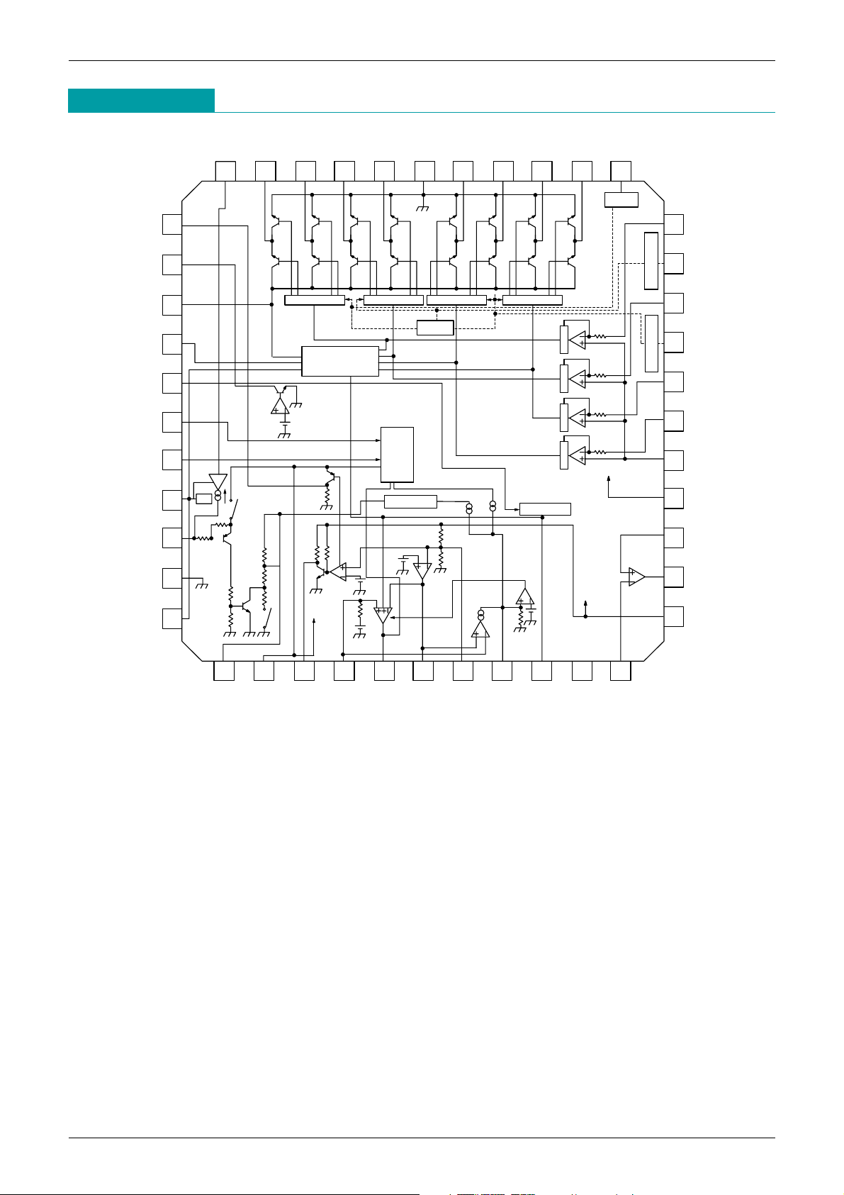
This driver IC contains a 4ch H bridge driver and DC-DC converter control circuit on one chip, and was
developed for use in portable CD players. QFP-44 is used for the package, making it ideal for smaller sets.
Features
(1) Built-in 4ch H bridge driver, and PWM control of load drive voltage is made possible by external
components.
(2) DC-DC converter control circuit on chip.
(3) With reset output inversion output pin.
(4) Empty detection level can be switched between rechargeable battery and dry battery.
(5) Constant current charging; current value can be varied using external resistor.
(6) Built-in power transistor for charging.
(7) Built-in independent thermal shutdown circuit.
Package
QFP-44
Applications
Portable CD radio cassette recorders
Page 2
MITSUMI
4ch Moter driver IC for Portable CD Player
Block Diagram
33
34
22
21
20
19
18
17
16
15
14
13
12
35
36
37
38
39
40
41
42
43
44
1 2 3 4 5 6 7 8 9 10 11
32 31 30 29 28 27 26 25 24 23
AMUTE
EMP
HVcc
PSW
CLK
START
OFF
CHGVcc
SEL
PREGND
PWMFIL
IN1
MUTE2
IN2
MUTE34
IN4
IN3
Vref
VSYS2
OP+
OP
OUT
VSYS1
RCHG OUTIR OUT1F OUT2R OUT2F POWGND OUT3F OUT3R OUT4F OUT4R BRAKE1
BSEN BATT RESET DEAD SW EO EI SPRT CT N.C. OP
-
V
I
/
V
I
/
V
I
/
V
I
/
BRAKE1
BTL
BTL
BTL
BTL
POWER
OFF
STARTER
MAXIMUM
DETECTION
CLK
TSD
TRIANGLE WAVE
OVER-VOLTAGE
PRE
-
DRIVER POWER SUPPLY
TSD
POWER UNIT
POWER SUPPLY
CONTROL CIRCUIT
POWER SUPPLY
MUTE2
MUTE34
Page 3
MITSUMI
4ch Moter driver IC for Portable CD Player
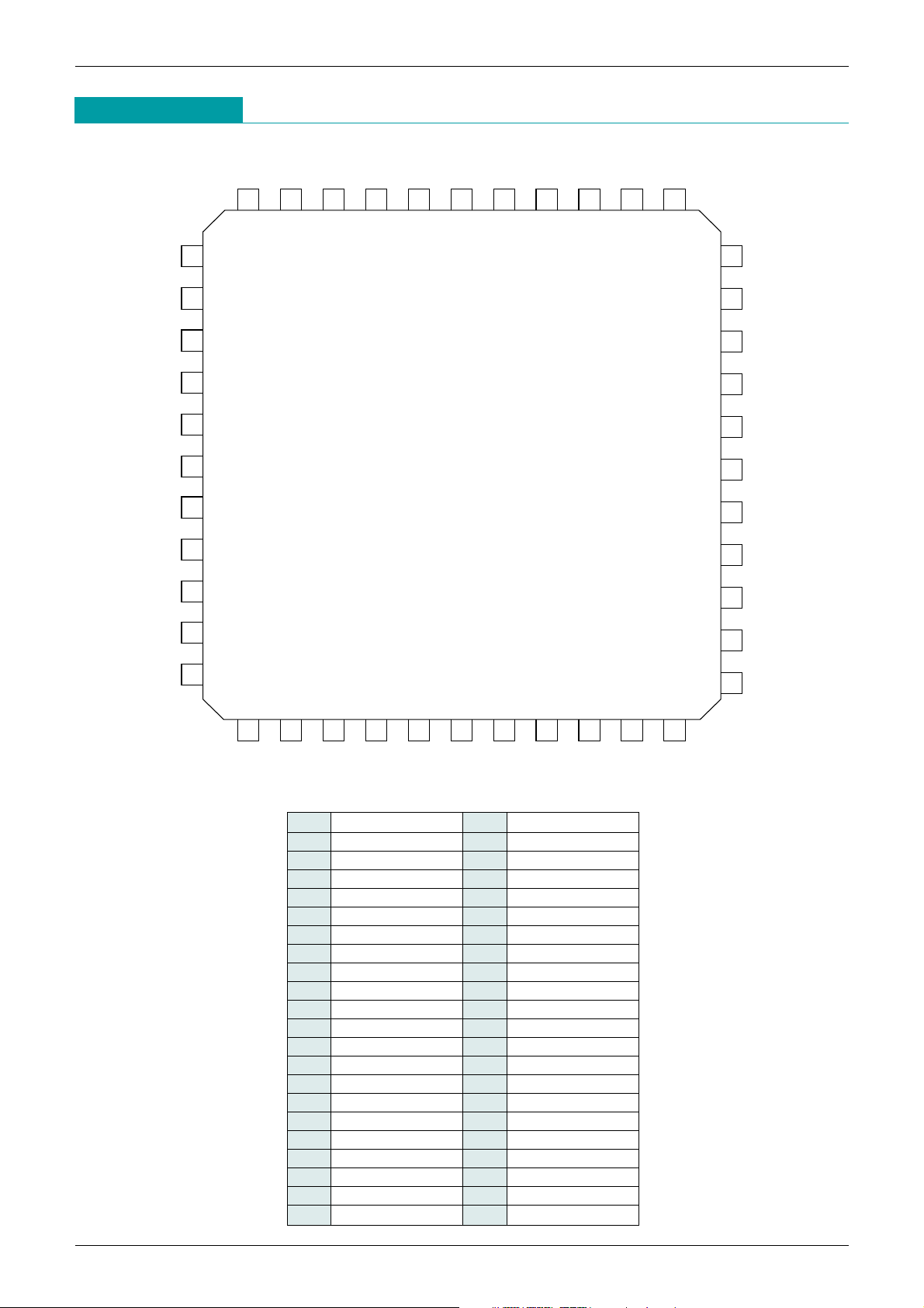
Pin Assignment
AMUTE
RCHG OUT1R OUT1F OUT2R OUT2F OUT3F OUT3R OUT4F OUT4R BRAKE1
POWGND
BSEN BATT RESET DEAD SW EI SPRT CT N.C. OP
-
EO
1 2 3 4 5 7 8 9 10 116
33
34
35
36
37
38
39
40
41
42
43
44
22
21
20
19
18
17
16
15
14
13
12
32 31 30
MM1538XQ
29 27 26 25 24 2328
EMP
HV
CC
PSW
CLK
START
OFF
CHGV
CC
SEL
PREGND
PWMFIL
IN1
MUTE2
IN2
MUTE34
IN4
IN3
Vref
VSYS2
OP+
OPOUT
VSYS1
1 BSEN 23 BRAKE1
2 BATT 24 OUT4R
3 RESET 25 OUT4F
4 DEAD 26 OUT3R
5 SW 27 OUT3F
6 EO 28 POWGND
7 EI 29 OUT2F
8 SPRT 30 OUT2R
9 C
T 31 OUT1F
10 N.C. 32 OUT4R
11 OP
-
33 RCHG
12 VSYS1 34 AMUTE
13 OPOUT 35 EMP
14 OP+ 36 HV
CC
15 VSYS2 37 PSW
16 Vref 38 CLK
17 IN3 39 START
18 IN4 40 OFF
19 MUTE34 41 CHGV
CC
20 IN2 42 SEL
21 MUTE2 43 PREGND
22 IN1 44 PWMFIL
Page 4
MITSUMI
4ch Moter driver IC for Portable CD Player
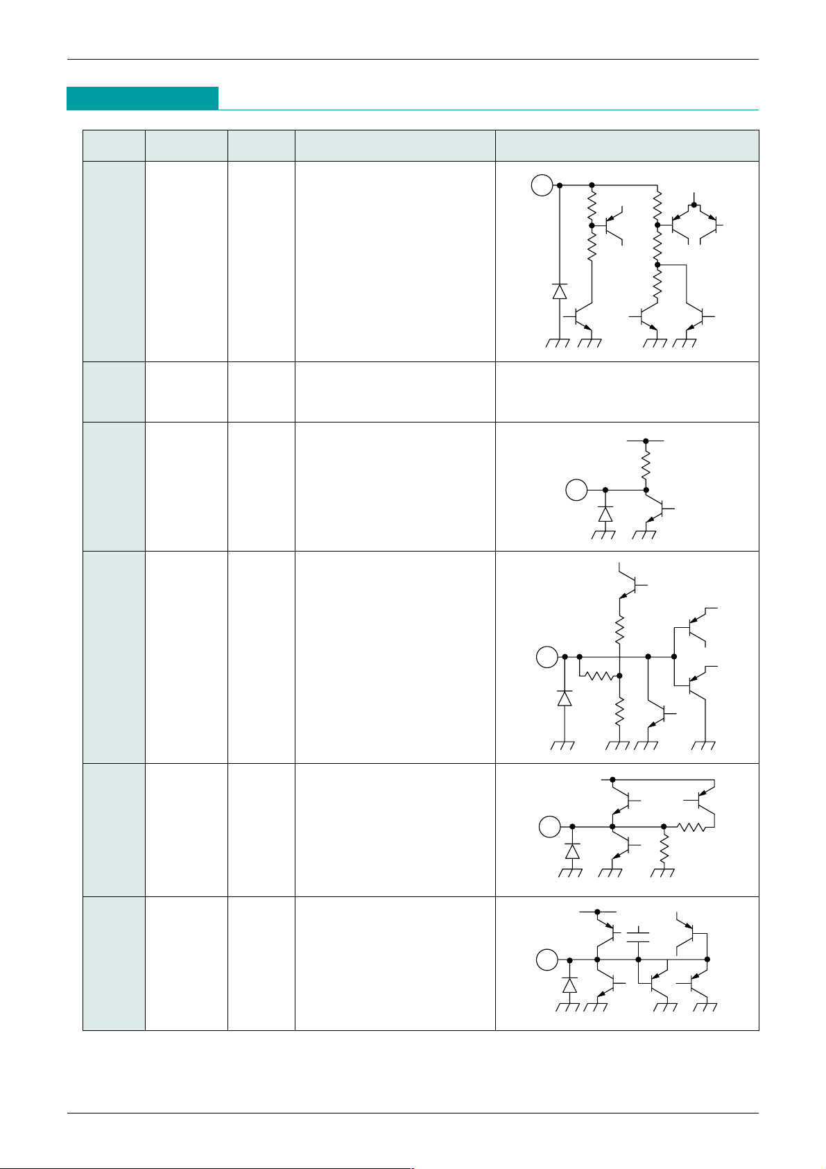
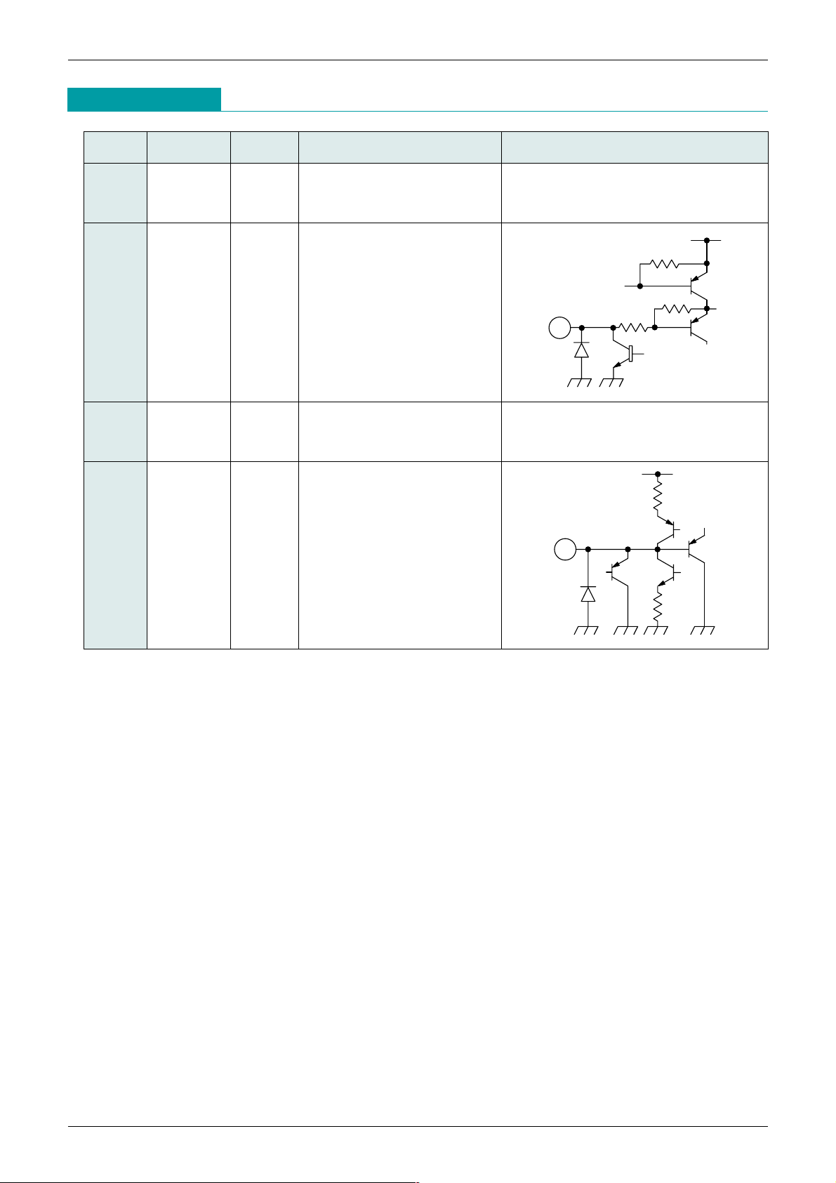
Pin No. Pin Name
Input/Output
Function Internal Equivalent Circuit
1 BSEN
Battery Voltage Monitor
1
71kΩ
16.5kΩ
20kΩ
10.5kΩ
14.85kΩ
Pin Description
Input
Battery Power Supply InputInput Power Supply
3 RESET Output Reset Detect Output
4
49kΩ
13kΩ
30.8kΩ
4 DEAD Input DEAD Time Setting
5 SW Output Transistor Drive For Voltage
Multiplier
3
90kΩ
VSYS1
2 BATT
6
VSYS1
6 EO Output Error Amplifier Output
BATT
5
150Ω
6kΩ
Page 5

MITSUMI
4ch Moter driver IC for Portable CD Player
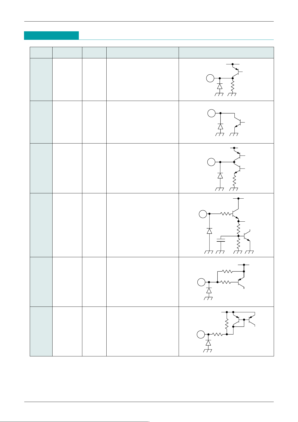
Pin No. Pin Name
Input/Output
Function Internal Equivalent Circuit
7 EI
Error Amplifier Input
35kΩ
21.6kΩ
7
VSYS1
Pin Description
Input
Short Circuit Protection
Setting
Output
9 CT Output Triangular
-
Wave Output
10 N.C.
11 OP
-
14 OP+
Input Op Amp Negative Input
Op Amp Positive Input
420kΩ
10kΩ
2kΩ
9
VSYS1
BATT
8 SPRT
220kΩ
8
VSYS1
12 VSYS1 Input Control Circuit Power Supply
Input
Control Circuit Power Supply
13
VSYS1
13 OPOUT Output Op Amp Output
14
11
Page 6

MITSUMI
4ch Moter driver IC for Portable CD Player
Pin No. Pin Name
Input/Output
Function Internal Equivalent Circuit
15 VSYS2
Driver Pre-step Power Supply
Pin Description
Input
Reference Voltage InputInput
17 IN3
18 IN4
20 IN2
22 IN1
Input ch3 Control Signal Input
ch4 Control Signal Input
ch2 Control Signal Input
ch1 Control Signal Input
68kΩ
68kΩ
19
21
23
19 MUTE34
21 MUTE2
23 BRAKE1
Input ch3 and 4 Mute
ch2 Mute
ch1 Brake
11kΩ
20PIN=7.5kΩ
17
18
20
22
16 Vref
16
24kΩ
50kΩ
200Ω
4
36
24
26
30
32
25
27
29
31
28
24 OUT4R
25 OUT4F
26 OUT3R
27 OUT3F
29 OUT2F
30 OUT2R
31 OUT1F
32 OUT1R
Output ch4 Negative Output
ch4 Positive Output
ch3 Negative Output
ch3 Positive Output
ch2 Positive Output
ch2 Negative Output
ch1 Positive Output
ch1 Negative Output
28 POWGND Power Block Power Supply
Ground
36 HVCC Input H-Bridge Power Supply Input
950Ω
33
33 RCHG Input Charge Current Setting
Pre
-
Drive Power Supply
Page 7
MITSUMI
4ch Moter driver IC for Portable CD Player
Pin No. Pin Name
Input/Output
Function Internal Equivalent Circuit
34 AMUTE
Reset Invert Output
34
95kΩ
BATT
Pin Description
Output
Empty Detect OutputOutput
37 PSW Output PWM Transistor Drive
38
2kΩ
50kΩ
100kΩ
VSYS1
38 CLK Input External Clock Synchronizing
Input
39 START Input Voltage Multiplier DC
-
DC
Converter Start
50Ω
37
BATT
35 EMP
35
40
180kΩ
27kΩ
VSYS1
40 OFF Input Voltage Multiplier DC-DC
Converter OFF
39
390kΩ
200kΩ
BATT
Page 8
MITSUMI
4ch Moter driver IC for Portable CD Player
Pin No. Pin Name
Input/Output
Function Internal Equivalent Circuit
41 CHGV
CC Charging Circuit Power Supply
Input
Pin Description
Input
Empty Detect Level SwitchInput
Output
43 PREGND Pre Section Power Supply
Ground
2kΩ
2kΩ
VSYS1
44
44 PWMFIL Input PWM Phase Compensation
42 SEL
200kΩ
130kΩ
15kΩ
42
BATT
Charging Circuit Power Supply
Pre Section Power Supply Ground
*
The positive and negative outputs are the polarity with respect to the input
Page 9

MITSUMI
4ch Moter driver IC for Portable CD Player
Absolute Maximam Ratings
(Ta=25°C)
Recommended Operating Conditions
Electrical Characteristics
(unless otherwise specified, Ta=25°C , BATT=2.4V, VSYS1=VSYS2=3.2V,Vref=1.6V,
CHGVcc=0V,fCLK=88.2kHz)
Item Symbol Min. Typ. Max. Unit
Control Circuit Power Supply Voltage
VSYS1 2.7 3.2 5.5 V
Pre-Driver Circuit Power Supply Voltage
VSYS2 2.7 3.2 5.5 V
H-Bridge Power Supply Voltage HV
CC PWM BATT V
Power Supply Voltage BATT 1.5 2.4 8.0 V
Charging circuit Power Supply Voltage
CHGVCC 3.0 4.5 8.0 V
Operating Temperature Ta –10 25 70 °C
Item Symbol Measurement Conditions Min. Typ. Max. Unit
<Common Section>
BATT Stand-by Current I
ST
BATT=9.0V, VSYS1=VSYS2=Vref=0V
03µA
BATT Supply Current (No load)
IBAT HVCC=0.45V, MUTE34=3.2V 2.5 4.0 mA
VSYS1 Supply Current (No load)
I
SYS1 HVCC
=
0.45V, MUTE34=3.2V, EI=0V 4.7 6.4 mA
VSYS2 Supply Current (No load)
ISYS2 HVCC=0.45V, MUTE34=3.2V 4.1 5.5 mA
CHGVcc Supply Current (No load)
ICGVCC CHGVCC=4.5V, ROUT=OPEN 0.65 2.00 mA
<H
-
Bridge Driver Part>
Voltage Gain ch1,ch3.ch4 G
VC134 12 14 16 dB
Voltage Gain ch2 G
VC2 21.5 23.5 24.5 dB
Gain Error By Polarity G
VC
-
20 2dB
Input pin resistance ch1,ch3,ch4
RIN134 IN=1.7V and 1.8V 9 11 13 kΩ
Input pin resistance ch2 R
IN2 IN
=
1.7V and 1.8V 6 7.5 9 kΩ
Maximum Output Voltage V
OUT
RL=8Ω, HVcc=BATT=4.0V, IN=0-3.2V
1.9 2.1 V
Saturation Voltage (Lower) V
satL Io
=-300mA, IN=0 and 3.2V 240 400 mV
Saturation Voltage (Upper) V
satU Io
=-300mA, IN=0 and 3.2V 240 400 mV
Input Offset Voltage V
OI
-
80 8mV
Output Offset Voltage ch1,ch3,ch4
VOO134 Vref=IN=1.6V
-
50 0 50 mV
Output Offset Voltage ch2 V
OO2 Vref
=IN=
1.6V
-
130 0 130 mV
Dead Zone V
DB
-
10 0 10 mV
BRAKE1ON Threshold Voltage
VBRON IN1=1.8V 2.0 V
BRAKE1OFF Threshold Voltage
VBROFF IN1=1.8V 0.8 V
MUTE2 ON Threshold Voltage
VM2ON IN2=1.8V 2.0 V
*1 Vcc shows input voltage of VSYS1,VSYS2,HVcc,BATT,and CHGVcc.
*2 Reduced by 5mW for each increase in Ta of 1°C over 25°C.
Item Symbol Rating Unit
Supply Voltage V
CC *1 13.5 V
Driver Output Current I
O 500 mA
Power Dissipation Pd 625 *2 mW
Operating Temperature T
OPR –30 ~ +85 °C
Storage Temperature T
STG –55 ~ +150 °C
Page 10

MITSUMI
4ch Moter driver IC for Portable CD Player
Electrical Characteristics
(unless otherwise specified, Ta=25°C , BATT=2.4V, VSYS1=VSYS2=3.2V,Vref=1.6V,
CHGVcc=0V,fCLK=88.2kHz)
Item Symbol Measurement Conditions Min. Typ. Max. Unit
<H
-
Bridge Driver Part>
MUTE2 OFF Threshold Voltage
VM2OFF IN2=1.8V 0.8 V
MUTE34 ON Threshold Voltage
VM34ON IN3=IN4=1.8V 0.8 V
MUTE34 OFF Threshold Voltage
VM34OFF IN3=IN4=1.8V 2.0 V
Vref ON Threshold Voltage V
refON IN1
=
IN2=IN3=IN4=1.8V 1.2 V
Vref OFF Threshold Voltage V
refOFF IN1
=
IN2=IN3=IN4=1.8V 0.8 V
BRAKE1 Brake Current I
BRAKE1
Current difference between BRAKE pin "H" time and "L" time.
4 7 10 mA
<PWM Power Supply Driving>
PSW Sink Current I
PSW IN1
=
2.1V 10 13 17 mA
HVcc Level Shift Voltage V
SHIF IN1
=
1.8V, HVCC-OUT1F 0.35 0.45 0.55 V
HVcc Leak Current I
HLK
HVCC=9.0V, VSYS1=VSYS2=BATT=0V
05µA
PWM Amp Transfer Gain G
PWM IN1
=
1.8V, HVCC=1.2 ~ 1.4V 1/60 1/50 1/40 1/kΩ
<DC
-
DC Converter>
<Error Amp>
VSYS1 Threshold Voltage V
S1TH 3.05 3.20 3.35 V
EO Pin Output Voltage "H" V
EOH EI
=
0.7V, Io=-
100µA 1.4 1.6 V
EO Pin Output Voltage "L" V
EOL EI
=
1.3V, Io=100µA 0.3 V
<Short Circuit Protection>
SPRT Pin Voltage V
SPR EI
=
1.3V 0 0.1 V
EO=H SPRT Pin Current1 I
SPR1 EI
=
0.7V 6 10 16 µA
OFF=L SPRT Pin Current2 I
SPR2 EI
=
1.3V, OFF=0V 12 20 32 µA
SPRT Pin Current3 Over-Voltage
ISPR3 EI=1.3V, BATT=9.5V 12 20 32 µA
SPRT Pin Impedance R
SPR 175 220 265 kΩ
SPRT Pin Threshold Voltage V
SPTH EI
=
0.7V, CT=0V 1.10 1.20 1.30 V
Over-Voltage Protection Detect
VHVPR BSEN Pin Voltage 8.0 8.4 9.0 V
<Transistor Driving>
SW Pin Output Voltage1 "H" V
SW1H
BATT=CT=1.5V, VSYS1=VSYS2=0V,
0.78 0.98 1.13 V
Io=-2mA
Starting Time
SW Pin Output Voltage2 "H" VSW2H
CT=0V, Io=-10mA, EI=0.7V, SPRT=0V
1.00 1.50 V
SW Pin Output Voltage2 "L" V
SW2L CT
=
2.0V, Io=10mA 0.30 0.45 V
SW Pin Oscillating Frequency1
fSW1
CT=470pF, VSYS1=VSYS2=0V Starting Time
65 80 95 kHz
SW Pin Oscillating Frequency2
f
SW2 CT
=
470pF, CLK=0V 60 70 82 kHz
SW Pin Oscillating Frequency3
fSW3 CT=470pF 88.2 kHz
SW Pin Minimum Pulse Width
TSWmin CT=470pF, EO=0.5V 0.7V Sweep 0.01 0.60 µs
Pulse Duty Start D
SW1 CT
=
470pF, VSYS1=VSYS2=0V 40 50 60 %
Max.Pulse Duty At Self-Running
DSW2 CT=470pF, EI=0.7V, CLK=0V 70 80 90 %
Max. Pulse Duty At CLK Synchronization
DSW3 CT=470pF, EI=0.7V 65 75 85 %
<Interface>
OFF Pin Threshold Voltage
VOFTH EI=1.3V
VSYS1-2.0
V
OFF Pin Bias Current I
OFF OFF
=
0V 75 95 115 µA
START Pin ON Threshold Voltage
V
STATH1 VSYS1
=
VSYS2=0V, CT=2.0V
BATT-1.0
V
START Pin OFF Threshold Voltage
VSTATH2 VSYS1=VSYS2=0V, CT=2.0V
BATT-0.3
V
Page 11

MITSUMI
4ch Moter driver IC for Portable CD Player
Electrical Characteristics
(unless otherwise specified, Ta=25°C , BATT=2.4V, VSYS1=VSYS2=3.2V,Vref=1.6V,
CHGVcc=0V,fCLK=88.2kHz)
Item Symbol Measurement Conditions Min. Typ. Max. Unit
<Interface>
START Pin Bias Current I
START START=0V
10 20 30
µA
13 16 19
CLK Pin Threshold Voltage"H"
VCLKTHH 2.0 V
CLK Pin Threshold Voltage"L"
VCLKTHL 0.8 V
CLK Pin Bias Current I
CLK CLK
=
3.2V 10 µA
<Dead Time>
DEAD Pin Impedance R
DEAD 52 65 78 kΩ
DEAD Pin Output Voltage V
DEAD 0.78 0.88 0.98 V
<Starter Circuit>
Starter Switching Voltage V
STNM VSYS1=VSYS2=0V 3.2V, START=0V 2.3 2.5 2.7 V
Starter Switching Hysteresis Width
VSNHS START=0V 130 200 300 mV
Discharge Release V
DIS 1.63 1.83 2.03 V
<Empty Detection>
EMP Detection Voltage 1 V
EMPT1 VSEL
=
0V 2.1 2.2 2.3 V
EMP Detection Voltage 2 V
EMPT2 ISEL
=-2µA 1.7 1.8 1.9 V
EMP Detection Hysteresis Voltage 1
VEMHS1 VSEL=0V 25 50 100 mV
EMP Detection Hysteresis Voltage 2
VEMHS2 ISEL=-
2µA 25 50 100 mV
EMP Pin Output Voltage V
EMP Io
=
1mA, BSEN=1V 0.5 V
EMP Pin Output Leak Current
IEMPL BSEN=2.4V 1.0 µA
BSEN Pin Input Resistance R
BSEN VSEL
=
0V 17 23 27 kΩ
BSEN Pin Leak Current I
BSENL VSYS1
=
VSYS2=0V, BSEN=4.5V 1.0 µA
SEL Pin Detection Voltage V
SELTH VSELTH
=
BATT-SEL, BSEN=2.0V 1.5 V
SEL Pin Detection Current I
SELT
-
2µA
<Reset Circuit>
VSYS1 RESET Threshold Voltage Ratio
HSRT
Comparison with error amplifier threshold voltage
85 90 95 %
RESET Detection Hysteresis Width
VRSTHS 25 50 100 mV
RESET Pin Output Voltage V
RST Io
=
1mA, VSYS1=VSYS2=2.8V 0.5 V
RESET Pin PULL UP Resistance
RRST 72 90 108 kΩ
AMUTE Pin Output Voltage 1
VAMT1 Io=-
1mA, VSYS1=VSYS2=2.8V
BATT-0.4
BATT
V
AMUTE Pin Output Voltage 2
VAMT2
Io=-1mA, START=0V, VSYS1=VSYS2=0V
BATT-0.4
BATT
V
AMUTE Pin PULL DOWN Resistance
RAMT 77 95 113 kΩ
<Op Amp>
Input Bias Current I
BIAS OP+
=
1.6V 300 nA
Input Offset Voltage V
OIOP
-
5.5 0 5.5 mV
High Level Output Voltage V
OHOP RL
=
OPEN 2.8 V
Low level Output Voltage V
OLOP RL
=
OPEN 0.2 V
Output Drive Current (Source)
ISOU 50Ω GND
-
6.5-3.0 mA
Output Drive Current (Sink)
ISIN 50Ω VSYS1 0.4 0.7 mA
Open Loop Voltage Gain GVO V
IN
=-75dBV, f=1kHz 70 dB
Slew Rate SR 0.5 V/µs
<Battery Charging Circuit>
RCHG Pin Bias Voltage V
RCHG CHGVCC
=
4.5V, RCHG=1.8kΩ 0.71 0.81 0.91 V
Page 12

MITSUMI
4ch Moter driver IC for Portable CD Player
Electrical Characteristics
(unless otherwise specified, Ta=25°C , BATT=2.4V, VSYS1=VSYS2=3.2V,Vref=1.6V,
CHGVcc=0V,fCLK=88.2kHz)
Item Symbol Measurement Conditions Min. Typ. Max. Unit
<Battery Charging Circuit>
RCHG Pin Output Resistance
RRCHG CHGVCC=4.5V, RCHG=0.5 and 0.6V 0.75 0.95 1.20 kΩ
SEL Pin Leak Current 1 I
SELLK1
CHGVCC=4.5V, RCHG=OPEN, BATT=4.5V
1.0 µA
SEL Pin Leak Current 2 I
SELLK2
CHGVCC=0.6V, RCHG=1.8kΩ, BATT=4.5V
1.0 µA
SEL Pin Saturation Voltage V
SELCG
CHGVCC=4.5V, Io=300mA, RCHG=0Ω
0.45 1.00 V
Measuring Circuit
AMUTE
EMP
HVcc
PSW
CLK
START
OFF
CHGVCC
SEL
PREGND
PWMFIL
RCHG
OUT1R
OUT1F
OUT2R
OUT2F
POWGND
OUT3F
OUT3R
OUT4F
OUT4R
BRAKE1
33 32 31 30 29 28 27 26 25 24 23
34
35
36
37
38
39
40
41
42
43
44
1 2 3 4 5 6 7 8 9 10 11
22
21
20
19
18
17
16
15
14
13
12
IN1
MUTE2
IN2
MUTE34
IN4
IN3
Vref
VSYS2
OP+
OP
OUT
VSYS1
MM1538XQ
BSEN
BATT
RESET
DEADSWEO
EI
SPRT
Ct
N.C
OP
-
A
V
V
AA
V
A
V
A
V
V
V
A
A
A
V
V
A
A
V
V
V
V
A
a
a
a
a
b
b
b
b
SW16
SW15
SW14
SW13
10µ
1k
SW12
V
SW11
a
a
d
c
b
b
50
V
A
V
V
SW19
1.8k
SW20
a
b
a
b
c
a
b
a
b
b
b
b
a
a
a
a
a
V
V
V
a
ba
b
B
R F
SW18 SW17
SW21
47
51k
SW22
SW23
a
b
47µ
33µ
SW24
SW25
SW26
SW27
SW28
100k
2200p
10p
20k
100k
470µ
SW10
SW9
a
aaa
a
a
a
a
aa
bb
b
b
b
b
b
SW1
SW2
SW3ASW4
VVV
SW5 SW6
10k
10k
SW7
SW8
470p
1M
V
frequency
100µ
A A A
A
A
A A A
A
Page 13

MITSUMI
4ch Moter driver IC for Portable CD Player
Switching Position Table
Item
SW No.
1 4 5 6 7 8 22 24 25 26
BATT Stand-by Current
----------
BATT Supply Current (No load)
------
a
-
a
-
VSYS1 Supply Current (No load)
---
a
--
a
-
a
-
VSYS2 Supply Current (No load)
------
a
-
a
-
CHGVcc Supply Current (Noload)
----------
VSYS1 Threshold Voltage
--
a
-------
EO Pin Output Voltage "H"
--
aa
------
EO Pin Output Voltage "L"
--
aa
------
SPRT Pin Voltage
---
aa
-----
SPRT Pin Current1 EO="H"
---
ab
-----
SPRT Pin Current2 OFF="L"
---
ab
----
a
SPRT Pin Current3 Over-Voltage a
--
ab
-----
SPRT Pin Impedance
----
b
-----
SPRT Pin Threshold Voltage
---
aaa
----
Over-Voltage Protection Detect a
---
a
-----
SW Pin Output Voltage1 "H"
-
a
---
a
--
a
-
SW Pin Output Voltage2 "H"
-
a
-
aba
----
SW Pin Output Voltage2 "L"
-
a
---
a
----
SW Pin Oscillating Frequency 1
-
b
---
b
--
a
-
SW Pin Oscillating Frequency 2
-
b
---
b
-
b
--
SW Pin Oscillating Frequency 3
-
b
---
b
-
a
--
SW Pin Minimum Pulse Width
-
bb
--
b
----
Pulse Duty Start
-
b
---
b
-
ba
-
Max. Pulse Duty At Self-Running
-
b
---
b
-
b
--
Max. Pulse Duty At CLK Synchronization-b
-
a
-
b
-
a
--
-
: Turn off switch
Page 14

MITSUMI
4ch Moter driver IC for Portable CD Player
Switching Position Table
Item
SW No.
2 3 4 6 7 8 20 24 25 26
DEAD Pin Impedance
-
b
--------
DEAD Pin Output Voltage
-
a
--------
OFF Pin Threshold Voltage
---
aa
----
a
OFF Pin Bias Current
---------
a
START Pin ON Threshold Voltage
--
a
--
a
--
a
-
START Pin OFF Threshold Voltage
--
a
--
a
--
a
-
START Pin Bias Current
--------
a
-
CLK Pin Threshold Voltage"H"
--
a
--
b
-
b
--
CLK Pin Threshold Voltage"L"
--
a
--
b
-
b
--
CLK Pin Bias Current
-------
a
--
Starter Switching Voltage
--
a
-----
a
-
Starter Switching Hysteresis Width
--
a
-----
a
-
Discharge Release Voltage
----
a
-----
VSYS1 Pin RESET Threshold
b
---------
Voltage Ratio
RESET Detection Hysteresis Width
b
---------
RESET Pin Output voltage b
---------
RESET Pin PULL UP Resistance a
---------
AMUTE Pin Output Voltage 1
------
b
---
AMUTE Pin Output Voltage 2
------
b
-
a
-
AMUTE Pin PULL DOWN Resistance
------
a
---
-
: Turn off switch
Page 15

MITSUMI
4ch Moter driver IC for Portable CD Player
Switching Position Table
Item
SW No.
1 9 10 11 12 21 27
EMP Detection Voltage 1 a
----
aa
EMP Detection Voltage 2 a
----
ab
EMP Detection Hysteresis Voltage 1 aa
---
aa
EMP Detection Hysteresis Voltage 2 a
----
ab
EMP Pin Output Voltage a
----
b
-
EMP Pin Output Leak Current a
----
c
-
BSEN Pin Input Resistance a
-----
a
BSEN Pin Leak Current a
------
SEL Pin Detection Voltage a
----
aa
SEL Pin Detection Current a
----
ab
Input Bias Current
--
a
----
Input Offset Voltage
--
d
----
"H" Level Output Voltage
-
bc
----
"L" Level Output Voltage
-
ac
----
Output Drive Current (Source)
-
db
---
Output Drive Current (Sink)
--
da
---
Open Loop Voltage Gain
--
b
-
a
--
Slew Rate
--
d
-
a
--
-
: Turn off switch
Page 16

MITSUMI
4ch Moter driver IC for Portable CD Player
Switching Position Table
Item
SW No.
13 14 15 16 17 18 22
ch1R
---
bbba
Voltage Gain
ch2R
--
b
-
bba
ch3R b
---
bba
ch4R
-
b
--
bba
ch1
---
bbba
Gain Error By Polarity
ch2
--
b
-
bba
ch3 b
---
bba
ch4
-
b
--
bba
ch1
---
bbba
Input pin resistance
ch2
--
b
-
bba
ch3 b
---
bba
ch4
-
b
--
bba
ch1R
---
bbba
Maximum Output Voltage
ch2R
--
b
-
bba
ch3R b
---
bba
ch4R
-
b
--
bba
ch1F
--
ba
-
a
ch1R
--
b
-
aa
ch2F
-
b
-
a
-
a
Saturation Voltage (Lower)
ch2R
-
b
--
aa
ch3F b
--
a
-
a
ch3R b
---
aa
ch4F
-
b
--
a
-
a
ch4R
-
b
---
aa
ch1F
---
ba
-
a
ch1R
---
b
-
aa
ch2F
--
b
-
a
-
a
Saturation Voltage (Upper)
ch2R
--
b
--
aa
ch3F b
---
a
-
a
ch3R b
----
aa
ch4F
-
b
--
a
-
a
ch4R
-
b
---
aa
ch1
---
a
--
a
Input Offset Voltage
ch2
--
a
---
a
ch3 a
-----
a
ch4
-
a
----
a
ch1
---
bbba
Output Offset Voltage
ch2
--
b
-
bba
ch3 b
---
bba
ch4
-
b
--
bba
ch1
---
bbba
Dead Zone
ch2
--
b
-
bba
ch3 b
---
bba
ch4
-
b
--
bba
-
: Turn off switch
Page 17

MITSUMI
4ch Moter driver IC for Portable CD Player
Switching Position Table
Item
SW No.
19 27
CHGSET Pin Bias Voltage a
-
CHGSET Pin Output Resistance b
-
SEL Pin Leak Current 1
-
a
SEL Pin Leak Current 2 aa
SEL Pin Saturation Voltage bb
-
: Turn off switch
Item
SW No.
13 14 15 16 17 18 22 23 28
BRAKE1 ON Voltage ch1
---
bbba
--
BRAKE1 OFF Voltage ch1
---
bbba
--
MUTE2 ON Voltage ch2
--
b
-
bba
--
MUTE2 OFF Voltage ch2
--
b
-
bba
--
MUTE34 ON Voltage
ch3 b
---
bba
--
ch4
-
b
--
bba
--
MUTE34 OFF Voltage
ch3 b
---
bba
--
ch4
-
b
--
bba
--
ch1
---
bbba
--
Vref ON Voltage
ch2
--
b
-
bba
--
ch3 b
---
bba
--
ch4
-
b
--
bba
--
ch1
---
bbba
--
Vref OFF Voltage
ch2
--
b
-
bba
--
ch3 b
---
bba
--
ch4
-
b
--
bba
--
BREAK1 Brake Current ch1
---
bbba
--
PWM Sink Current
---
b
--
aba
HV
CC Level Shift Voltage
---
bbbbab
HV
CC Leak Current
----
bba
--
PWM Amp Transfer Gain
---
bbba
--
Page 18

MITSUMI
4ch Moter driver IC for Portable CD Player
Switching Position Table
VO4 VO3
VIN1
VIN3
VO2 VO1
Dead Zone
Output Offset Voltage
V
IN4
V
IN2
XC' XC
Output voltage:VO(mV)
Input voltage:VIN(mV)
Voltage Gain
G
VC (+)=20 log VO1
-
VO2
V
IN1
-
VIN2
G
VC (
-
)=20 log VO3-VO4
V
IN3
-
VIN4
Gain Error By Polarity
G
VC=GVC (+)
-
GVC (-)
Dead Zone
XC
-
XC'= VIN2·VO1-VIN1·VO2 -VIN3·VO4-VIN4·VO3
VO1
-
VO2 VO3-VO4
Page 19

MITSUMI
4ch Moter driver IC for Portable CD Player
Application Circuit
MM
33
34
22
21
20
19
18
17
16
15
14
13
12
35
36
37
38
39
40
41
42
43
44
1 2
3
4 5 6 7 8 9 10 11
32 31 30 29 28 27
26
25 24 23
AMUTE
EMP
HVcc
PSW
CLK
START
OFF
CHGVcc
SEL
PREGND
PWMFIL
IN1
MUTE2
IN2
MUTE34
IN4
IN3
Vref
VSYS2
OP+
OPOUT
VSYS1
BRAKE1
POWER
OFF
STARTER
MAXIMUM
DETECTION
CLK
0.1µ
0.1µ
47µ
47
33µ
TSD
TRIANGLE WAVE
OVER-VOLTAGE
PRE-DRIVER POWER SUPPLY
TSD
CONTROL CIRCUIT
POWER SUPPLY
RCHG
OUTIR
OUT1F
OUT2R
OUT2F
POWGND
OUT3F
OUT3R
OUT4F
OUT4R
BRAKE1
BSEN
BATT
RESET
DEAD
SW
EO
EI
SPRT
C
T
N.C.
OP
-
TRAVERSE
SPINDLE
FOCUS
TRACKING
BTL BTL BTL BTL
MUTE2
MUTE34
FILTER
1.8k
0.1µ 470p0.022µ8.2k
100µ
0.1µ
V
OUT
47µ
V
IN
10p
2200p
100k
100k
DC–DC
Converter
application
/
/
/
/
· We shall not be liable for any trouble or damege caused by using this circuit.
· In the event a problem which may affect industrial property or any other rights of us or a third party is
encountered during the use of information described in these circuit, Mitsumi Electric Co., Ltd. shall not be
liable for any such problem, nor grant a license therefor.
Page 20

MITSUMI
4ch Moter driver IC for Portable CD Player
Circuit operation
1 H-bridge driver block
(1) Gain setting
· The driver input resistance (ch 1,3 and 4) are 11kΩ typ. ,ch2 is 7.5kΩ typ. . Set the gain according to the
following formula.
· The driver output stage power supply is HVcc(36PIN), and the bridge circuit power supply is VSYS2
(15PIN). Connect a bypass capacitor between these two power supplies(approximately 0.1µF).
(2) Mute function
· Of the four drivers,ch1 has a brake function,and the other channels have a mute function.
· When BRAKE1(23PIN)is set to high level, both ch1 outputs go low level, and the circuit enters brake mode.
· When MUTE2(21PIN)is set to high level, the ch2 output is muted.
· When MUTE34(19PIN)is set to high level, the ch3 and 4 outputs are muted.
(3) Vref drop mute
· When the voltage applied to Vref(16PIN)is 1.0V or less typ. , the driver outputs are set to high impedance.
(4) Thermal shutdown
· When the chip temperature reaches 150°C typ. the output current is cut. The chip starts operating again at
about 120°C typ. .
2 PWM power supply drive block
· This detects the maximun output level from among the four channels, and supplies the load drive power
supply(36PIN)for the PWM. The external components are a PNP transistor, coil, Schottky diode,and
capacitor.
100kΩ
47kΩ
PSW
BATT
44 37 36
HVCC
SBD
47µF
33µH
PWMFIL
0.1µF
2200pF
10pF
ch1
ch2 GV=20log
55k
(db)
ch3
11k
+R
ch2 GV=20log
110k
(db)
7.5k
+R
R:Externally-connected input
Page 21

MITSUMI
4ch Moter driver IC for Portable CD Player
3 DC-DC converter block
(1) Output voltage
· 3.2V typ. voltage multiplier circuit can be constructed using external components. This voltage can be
varied with the addition of an external resistor. The setting method is as follows.
R1 · R3 + R2 · R4
VSYS1=1.2
R1+R3 R2+R4
(V)
R2 · R4
R2+R4
(2) Short protect function
· When the error amplifier output(6PIN)has switched to the high-level state,SPRT(8PIN)is charged, and when
the voltage reaches 1.2V typ. , the SW(5PIN)switching stops.The time until switching stops is set by the
capacitor connected to SPRT(8PIN)according to the following formula.
t=CSPRT
V
TH
(sec) (VTH=1.2V, ISPRT=10µA)
ISPRT
(3) Soft start function
· The soft start function operates when a capacitor is connected between DEAD(4PIN)and GND.
Also, the maximum duty can be varied by connecting a resistor to 4PIN.
t=CDEAD R (sec) (R=65kΩ)
(4) Power off function
· When low-level is applied to OFF(40PIN), SPRT(8PIN)is charged, and when the voltage reaches 1.2V typ. ,
the SW(5PIN)switching stops. The time until switching stops is set by the capacitor connected to
SPRT(8PIN)according to the following formula.
t=CSPRT
V
TH
(sec) (VTH=1.2V, IOFF=20µA)
I
OFF
R3
R4
12
7
EI
R1
R2
1.2V
R1=external resistor
R2=external resistor
R3=35kΩ
R4=21kΩ
VSYS1
Page 22

MITSUMI
4ch Moter driver IC for Portable CD Player
(5) Over voltage protection circuit
· When the voltage applied to BSEN(1PIN)reaches 8.4V typ. , SPRT(8PIN)is charged, and when the voltage
reaches 1.2V typ. , theSW(5PIN)switching stops. The time until switching stops is set by the capacitor
connected to SPRT(8PIN)according to the following formula.
t=CSPRT
V
TH
(sec) (VTH=1.2V, IHV=20µA)
IHV
4 Empty detector block
(1) Output voltage
· When the voltage applied to the BSEN(1PIN)falls below the detector voltage, EMP(35PIN)goes from high
level to low level(open-collector output). The detector voltage has 50mV typ. of hysteresis to prevent
output chattering. Use SEL(42PIN)to switch the detection voltage as shown below.
5 Reset circuit block
· At about 90% typ. of the DC-DC converter output voltage, RESET(3PIN)goes from low level to high level,
and AMUTE(34PIN)goes from high level to low level. The reset voltage has 50mV typ. of hysteresis to
prevent output chattering.
6 Charging circuit block
· The power supply for the charging circuit block is CHGV
CC(41PIN), and is independent from the other
circuits.The resistance between RCHG(33PIN)and GND sets the charging current. This current is drawn
from SEL(42PIN).
· A thermal shutdown circuit is provided,and when the chip temperature reaches 150°C typ. the charging
current is cut. The chip starts operating again at about 120°C typ. .
SEL Detect Voltage Return Voltage
L 2.20V typ. 2.25V typ.
High-Z 1.80V typ. 1.85V typ.
Page 23

MITSUMI
4ch Moter driver IC for Portable CD Player
Characteristics
Input voltage:VIN(V)
3
2
1
0
-1
-2
-3
-0.8 -0.6 -0.4 -0.2 0 0.2
20Ω
RL=∞
•
Ta=normal temperature
•
BATT=HVCC=4V
•
VSYS1=VSYS2=3.2V
•
Vref=1.6V
8Ω4Ω
4Ω
8Ω
20Ω
∞
0.80.4 0.6
Output voltage:VO(V)
Input voltage:VIN(V)
3
2
1
0
-1
-2
-3
-0.8 -0.6 -0.4 -0.2 0 0.2
20Ω
RL=∞
•
Ta=normal temperature
•
BATT=HVCC=4V
•
VSYS1=VSYS2=3.2V
•
Vref=1.6V
8Ω4Ω
4Ω8Ω20Ω
∞
0.80.4 0.6
Output voltage:VO(V)
Out voltage:VO(mV)
0.006
0.004
0.002
0
-0.002
-0.004
-0.006
-30 -20 -10 0 10
20Ω
•
Ta=normal temperature
•
BATT=HVCC=4V
•
VSYS1=VSYS2=3.2V
•
Vref=1.6V
8Ω
4Ω
4Ω
8Ω
20Ω
3020
Input voltage:VIN(mV)
Input Load Fluctuation
Input Load Fluctuation (ch2)
Daed Zone
Page 24

MITSUMI
4ch Moter driver IC for Portable CD Player
Characteristics
Control Circuit Power Supply voltage:VSYS1(V)
2.0
1.8
1.6
1.4
1.2
1.0
0.8
0.6
0.4
0.2
0
0 0.5 1.0 1.5 2.0 2.5
Ta=
normal temperature
BATT=2.4V
EO PIN
DAED PIN
4.03.0 3.5
Dead Output voltageE:VDAED(V)
Eo Output voltage:VEO(V)
Control Circuit Power Supply voltage:VSYS1(V)
4.5
4.0
3.5
3.0
2.5
2.0
1.5
1.0
0.5
0
0 0.5 1.0 1.5 2.0 2.5
Ta=
normal temperature
BATT=2.4V
4.03.0 3.5
Reset Output voltage:VRST(V)
Error Amp Output Voltage
Resete Pin Voltage
 Loading...