

Page 1
MITSUMI
Video Switch · 75Ω driver · Y/C mix MM1501
Video Switch · 75Ω driver · Y/C mix
Monolithic IC MM1501 Series
Outline
This IC extends the series of ICs for video/audio signal switching, with a 2-input 1-output single video switch,
video signal/chroma signal 75Ω driver, and Y/C mixing circuit in one small package (SOT-26).
Features
(1) Low power consumption achieved.
(2) Low power supply voltage realized.
(3) Frequency bandwidth without 75Ω driver: 10MHz with 75Ω driver: 7MHz
(4) Cross talk 70dB When 4.43MHz
(5) With SAG measures pin (75Ω driver and Y/C mix driver)
Package
SOT-26A (with 75Ω driver)
SOT-26B (without 75Ω driver)
Applications
(1) TV
(2) VTR
(3) Video camera
(4) Digital still camera
(5) Other visual equipment
Line-up
Functions
Switch
Driver
Y/C mix
Model Name
MM1501 4.5~13.0V
MM1502 4.5~13.0V
MM1503 4.5~13.0V
MM1504
MM1505 4.5~13.0V
MM1506 4.5~13.0V
MM1507 4.5~13.0V
MM1508 4.5~13.0V
MM1509
MM1510 4.5~13.0V
MM1511
MM1512 / 4.5~13.0V
Input
Output
21
11
11
Clamp 6dB amp 75Ω driver
/ 4.5~13.0V
SAG measures pin
Power supply
voltage
4.5~13.0V
4.5~13.0V
Page 2
MITSUMI
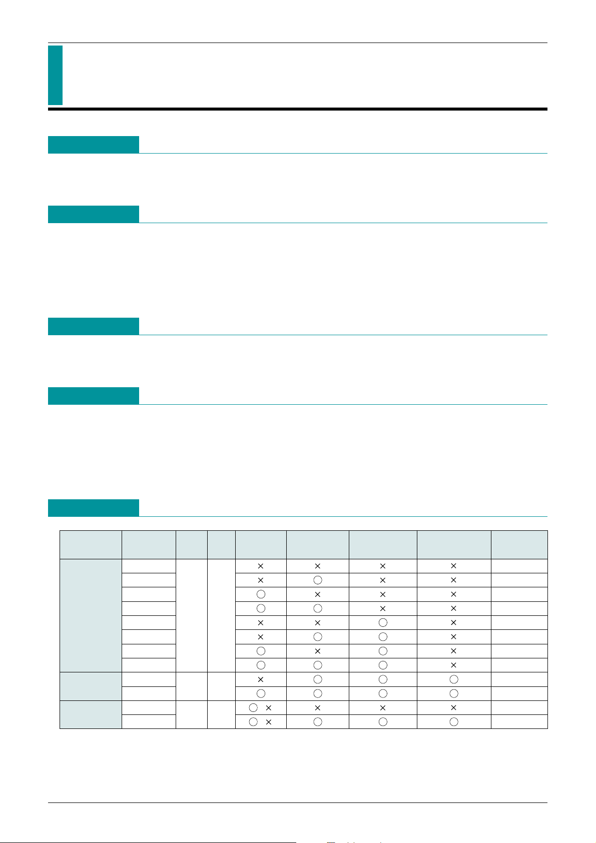
Block Diagram
MM1501 MM1502
Video Switch · 75Ω driver · Y/C mix MM1501
MM1503 MM1504
MM1505 MM1506
Page 3
MITSUMI
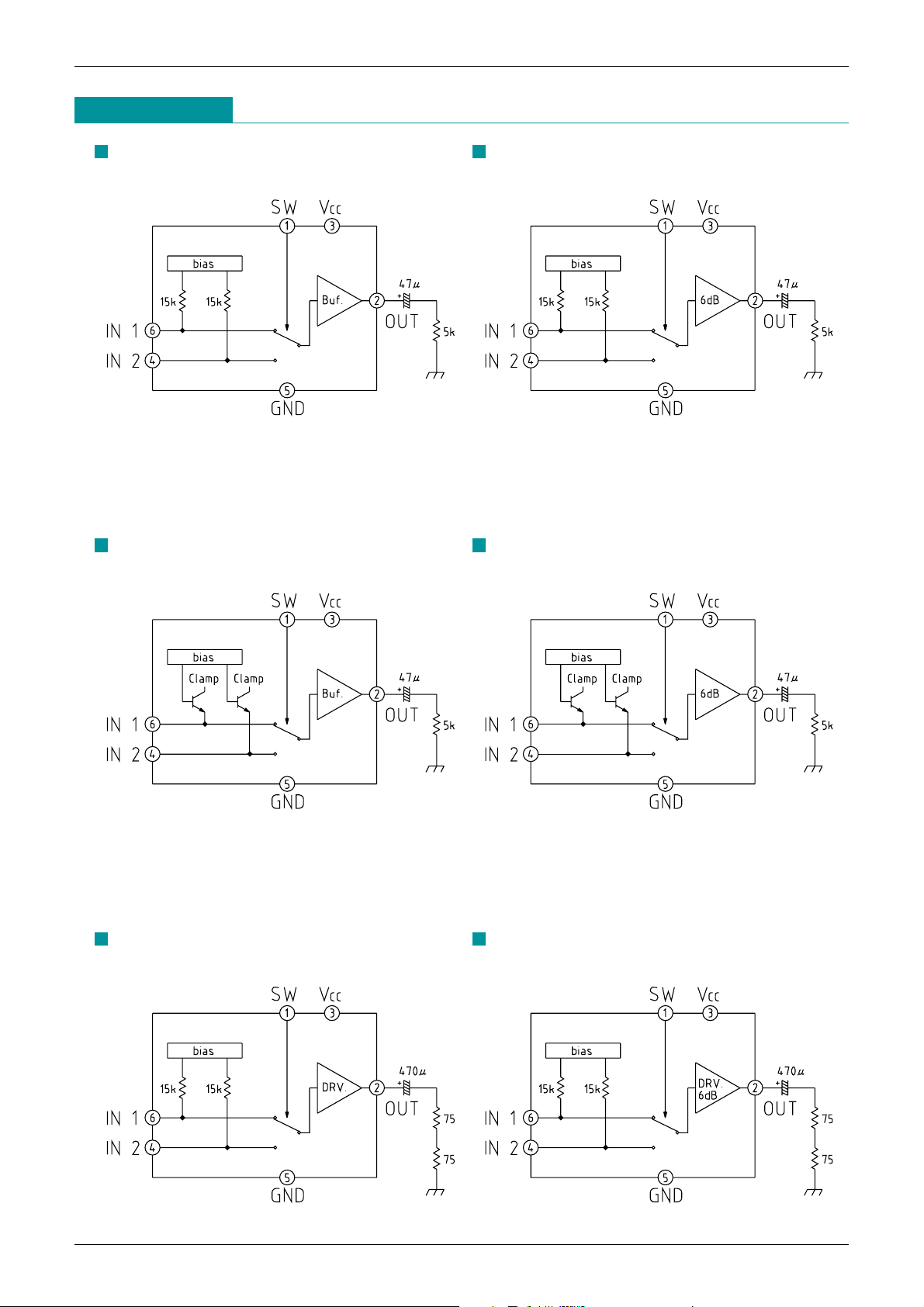
MM1507 MM1508
Video Switch · 75Ω driver · Y/C mix MM1501
MM1509 MM1510
MM1511 MM1512
Page 4
MITSUMI
Video Switch · 75Ω driver · Y/C mix MM1501
Absolute Maximum Ratings
(Ta=25°C)
Item Symbol Rating Unit
Storage temperature T
Operating temperature T
Power supply voltage V
Allowable loss
When alone Pd 200 mW
When mounted on board
STG
OPR
CC 15 V
-
40~+125 °C
-
30~+75 °C
Pd 350 (*)mW
Board size 100mm 100mm t=1.6
*
Recommended Operating Conditions
Item Symbol Rating Unit
Power supply voltage V
Electrical Characteristics
(Except where noted otherwise, Ta=25°C, VCC=5V)
MM1501
Item Symbol Measurement conditions Min. Typ. Max. Unit
Consumption current I
Input pin voltage V
Output pin voltage V
Voltage gain G
Frequency characteristic fc Refer to measurement procedures
Differential gain V
Differential phase V
CC=9V DG Refer to measurement procedures
CC=9V DP Refer to measurement procedures
Total harmonic distortion ratio
Output dynamic range V
Output offset voltage V
Cross talk C
SW input voltage H V
SW input voltage L V
Input impedance Zi 15 kΩ
Output impedance Zo 75 Ω
CC Refer to measurement procedures 3.7 4.8 mA
IN No-signal, no-load 2.70 2.90 3.10 V
OUT No-signal, no-load 2.15 V
V Refer to measurement procedures
THD Refer to measurement procedures 0.03 0.3 %
D Refer to measurement procedures 3.5 3.8 V
OFF Refer to measurement procedures ±15 mV
T Refer to measurement procedures
IH Refer to measurement procedures 2.1 V
IL Refer to measurement procedures 0.7 V
CC 4.5~13 V
-
0.5 0 +0.5 dB
-
10+1dB
-
30+3%
-
3 0 +3 deg
-
70-60 dB
MM1502
Item Symbol Measurement conditions Min. Typ. Max. Unit
Consumption current I
Input pin voltage V
Output pin voltage V
Voltage gain G
Frequency characteristic fc Refer to measurement procedures
Differential gain V
Differential phase V
CC=9V DG Refer to measurement procedures
CC=9V DP Refer to measurement procedures
Total harmonic distortion ratio
Output dynamic range V
Output offset voltage V
Cross talk C
SW input voltage H V
Sw input voltage L V
Input impedance Zi 15 kΩ
Output impedance Zo 12 Ω
CC Refer to measurement procedures 4.7 6.1 mA
IN No-signal, no-load 1.70 1.90 2.10 V
OUT No-signal, no-load 2.10 V
V Refer to measurement procedures 5.5 6.0 6.5 dB
-
10+1dB
-
30+3%
-
3 0 +3 deg
THD Refer to measurement procedures 0.03 0.3 %
D Refer to measurement procedures 3.5 3.8 V
OFF Refer to measurement procedures ±30 mV
T Refer to measurement procedures
IH Refer to measurement procedures 2.1 V
IL Refer to measurement procedures 0.7 V
-
70-60 dB
Page 5
MITSUMI
Video Switch · 75Ω driver · Y/C mix MM1501
MM1503
Item Symbol Measurement conditions Min. Typ. Max. Unit
Consumption current I
Input pin voltage V
Output pin voltage V
Voltage gain G
CC Refer to measurement procedures 3.3 4.3 mA
IN No-signal, no-load 1.80 2.00 2.20 V
OUT No-signal, no-load 1.25 V
V Refer to measurement procedures
Frequency characteristic fc Refer to measurement procedures
Differential gain DG Refer to measurement procedures
Differential phase DP Refer to measurement procedures
Total harmonic distortion ratio
Output dynamic range V
Output offset voltage V
Cross talk C
SW input voltage H V
SW input voltage L V
THD Refer to measurement procedures 0.03 0.3 %
D Refer to measurement procedures 2.6 2.9 V
OFF Refer to measurement procedures ±15 mV
T Refer to measurement procedures
IH Refer to measurement procedures 2.1 V
IL Refer to measurement procedures 0.7 V
Input impedance Zo 75 Ω
MM1504
Item Symbol Measurement conditions Min. Typ. Max. Unit
Consumption current I
Input pin voltage V
Output pin voltage V
Voltage gain G
Frequency characteristic fc Refer to measurement procedures
Differential gain DG Refer to measurement procedures
Differential phase DP Refer to measurement procedures
Total harmonic distortion ratio
Output dynamic range V
Output offset voltage V
Cross talk C
SW input voltage H V
SW input voltage L V
Input impedance Zo 12 Ω
CC Refer to measurement procedures 4.4 5.7 mA
IN No-signal, no-load 1.20 1.40 1.60 V
OUT No-signal, no-load 1.25 V
V Refer to measurement procedures 5.5 6.0 6.5 dB
THD Refer to measurement procedures 0.03 0.3 %
D Refer to measurement procedures 2.6 2.9 V
OFF Refer to measurement procedures ±30 mV
T Refer to measurement procedures
IH Refer to measurement procedures 2.1 V
IL Refer to measurement procedures 0.7 V
-
0.5 0 +0.5 dB
-
10+1dB
-
30+3%
-
3 0 +3 deg
-
70-60 dB
-
10+1dB
-
30+3%
-
3 0 +3 deg
-
70-60 dB
MM1505
Item Symbol Measurement conditions Min. Typ. Max. Unit
Consumption current I
Input pin voltage V
Output pin voltage V
Voltage gain G
Frequency characteristic fc Refer to measurement procedures
Differential gain V
Differential phase V
CC=9V DG Refer to measurement procedures
CC=9V DP Refer to measurement procedures
Output dynamic range V
Output offset voltage V
Cross talk C
SW input voltage H V
SW input voltage L V
Input impedance Zi 15 kΩ
CC Refer to measurement procedures 6.5 8.5 mA
IN No-signal, no-load 2.35 2.55 2.75 V
OUT No-signal, no-load 2.55 V
V Refer to measurement procedures
D Refer to measurement procedures 2.6 3.0 V
OFF Refer to measurement procedures ±15 mV
T Refer to measurement procedures
IH Refer to measurement procedures 2.1 V
IL Refer to measurement procedures 0.7 V
-
0.5 0.0 0.5 dB
-
10+1dB
-
30+3%
-
3 0 +3 deg
-
70-60 dB
Page 6

MITSUMI
Video Switch · 75Ω driver · Y/C mix MM1501
MM1506
Item Symbol Measurement conditions Min. Typ. Max. Unit
Consumption current I
Input pin voltage V
Output pin voltage V
Voltage gain G
CC Refer to measurement procedures 6.8 8.8 mA
IN No-signal, no-load 1.75 1.95 2.15 V
OUT No-signal, no-load 2.35 V
V Refer to measurement procedures 5.5 6.0 6.5 dB
Frequency characteristic fc Refer to measurement procedures
Differential gain V
Differential phase V
Output dynamic range V
Output offset voltage V
Cross talk C
SW input voltage H V
SW input voltage L V
CC=9V DG Refer to measurement procedures
CC=9V DP Refer to measurement procedures
D Refer to measurement procedures 3.0 3.3 V
OFF Refer to measurement procedures ±30 mV
T Refer to measurement procedures
IH Refer to measurement procedures 2.1 V
IL Refer to measurement procedures 0.7 V
Input impedance Zi 15 kΩ
MM1507
Item Symbol Measurement conditions Min. Typ. Max. Unit
Consumption current I
Input pin voltage V
Output pin voltage V
Voltage gain G
Frequency characteristic fc Refer to measurement procedures
Differential gain DG Refer to measurement procedures
Differential phase DP Refer to measurement procedures
Output dynamic range V
Output offset voltage V
Cross talk C
SW input voltage H V
SW input voltage L V
CC Refer to measurement procedures 6.4 8.3 mA
IN No-signal, no-load 1.15 1.35 1.55 V
OUT No-signal, no-load 1.35 V
V Refer to measurement procedures
D
OFF Refer to measurement procedures ±15 mV
T Refer to measurement procedures
IH Refer to measurement procedures 2.1 V
IL Refer to measurement procedures 0.7 V
Refer to measurement procedures 2.6 2.9 V
-
10+1dB
-
30+3%
-
3 0 +3 deg
-
70-60 dB
-
0.5 0 +0.5 dB
-
10+1dB
30+3%
-
-
3 0 +3 deg
-
70-60 dB
MM1508
Item Symbol Measurement conditions Min. Typ. Max. Unit
Consumption current I
Input pin voltage V
Output pin voltage V
Voltage gain G
Frequency characteristic fc Refer to measurement procedures
Differential gain DG Refer to measurement procedures
Differential phase DP Refer to measurement procedures
Output dynamic range V
Output offset voltage V
Cross talk C
SW input voltage H V
SW input voltage L V
CC Refer to measurement procedures 6.8 8.8 mA
IN No-signal, no-load 1.15 1.35 1.55 V
OUT No-signal, no-load 1.30 V
V Refer to measurement procedures 5.5 6.0 6.5 dB
D Refer to measurement procedures 2.6 3.0 V
OFF Refer to measurement procedures ±30 mV
T Refer to measurement procedures
IH Refer to measurement procedures 2.1 V
IL Refer to measurement procedures 0.7 V
-
10+1dB
-
30+3%
-
3 0 +3 deg
-
70-60 dB
Page 7

MITSUMI
Video Switch · 75Ω driver · Y/C mix MM1501
MM1509
Item Symbol Measurement conditions Min. Typ. Max. Unit
Consumption current I
Current consumption for PS I
PS input voltage L V
PS input voltage H V
Input pin voltage V
Output pin voltage V
Voltage gain G
CC1 Refer to measurement procedures 6.3 8.2 mA
CC2 Refer to measurement procedures 20 30 µA
PSL Refer to measurement procedures 0.3 V
PSH Refer to measurement procedures 1.8 V
IN No-signal, no-load 1.75 1.95 2.15 V
OUT No-signal, no-load 2.35 V
V Refer to measurement procedures 5.5 6.0 6.5 dB
Frequency characteristic fc Refer to measurement procedures
Differential gain V
Differential phase V
Output dynamic range V
CC=9V DG Refer to measurement procedures
CC=9V DP Refer to measurement procedures
D Refer to measurement procedures 2.9 3.2 V
Input impedance Zi 15 kΩ
MM1510
Item Symbol Measurement conditions Min. Typ. Max. Unit
Consumption current I
Current consumption for PS I
PS input voltage L V
PS input voltage H V
Input pin voltage V
Output pin voltage V
Voltage gain G
Frequency characteristic fc Refer to measurement procedures
Differential gain DG Refer to measurement procedures
Differential phase DP Refer to measurement procedures
Output dynamic range V
CC1 Refer to measurement procedures 6.4 8.3 mA
CC2 Refer to measurement procedures 20 30 µA
PSL Refer to measurement procedures 0.3 V
PSH Refer to measurement procedures 1.8 V
IN No-signal, no-load 1.15 1.35 1.55 V
OUT
V Refer to measurement procedures 5.5 6.0 6.5 dB
D Refer to measurement procedures 2.6 3.0 V
No-signal, no-load 1.15 V
-
10+1dB
-
30+3%
-
3 0 +3 deg
-
10+1dB
-
30+3%
-
3 0 +3 deg
MM1511
Item Symbol Measurement conditions Min. Typ. Max. Unit
Consumption current I
Y input pin voltage V
C input pin voltage V
Output pin voltage V
Voltage gain G
Frequency characteristic fc Refer to measurement procedures
Differential gain DG Refer to measurement procedures
Differential phase DP Refer to measurement procedures
Y output dynamic range V
C output dynamic range V
C input impedance Zi 15 kΩ
Output impedance Zo 25 Ω
CC Refer to measurement procedures 4.4 5.7 mA
YIN No-signal, no-load 2.00 2.20 2.40 V
CIN No-signal, no-load 1.85 2.05 2.25 V
OUT No-signal, no-load 1.15 V
V Refer to measurement procedures
DY Refer to measurement procedures 2.6 2.9 V
DC Refer to measurement procedures 2.0 V
-
0.5 0 6.5 dB
-
1 0 +0.5 dB
-
30+3%
-
3 0 +3 deg
Page 8

MITSUMI
Video Switch · 75Ω driver · Y/C mix MM1501
MM1512
Item Symbol Measurement conditions Min. Typ. Max. Unit
Consumption current I
Y input pin voltage V
C input pin voltage V
Output pin voltage V
Voltage gain G
CC Refer to measurement procedures 6.9 9.0 mA
YIN No-signal, no-load 1.95 2.15 2.35 V
CIN No-signal, no-load 1.80 2.00 2.20 V
OUT No-signal, no-load 1.10 V
V Refer to measurement procedures 5.5 6.0 6.5 dB
Frequency characteristic fc Refer to measurement procedures
Differential gain DG Refer to measurement procedures
Differential phase DP Refer to measurement procedures
Y output dynamic range V
C output dynamic range V
DY Refer to measurement procedures 2.6 2.9 V
DC Refer to measurement procedures 2.0 V
C input impedance Zi 15 kΩ
Measurement Procedures
MM1501~MM1508
· Switch Status
-
10+1dB
-
30+3%
-
3 0 +3 deg
Item
Consumption current I
Voltage gain G
Frequency characteristic
Differential gain DG
Differential phase DP
Symbol
Switch status
S1 S2 S3
CC 222
122
V
211
122
fc
211
122
211
122
211
Item
Total harmonic
distortion ratio 211
Symbol
THD
Output dynamic range V
Output offset voltage V
Cross talk C
SW input voltage H VIH
SW input voltage L V
Switch status
S1 S2 S3
122
122
D
211
222
OFF
221
121
T
212
221
IL
Page 9

MITSUMI
·Measurement Procedures (MM1501 ~ MM1504)
Video Switch · 75Ω driver · Y/C mix MM1501
Consumption current I
Voltage gain GV
CC
Connect a DC ammeter to VCC pin and measure. Hereafter, short
the ammeter to use.
Input a 2.0V
P-P (1.0VP-P for MM1502 and MM1504), 100kHz sine
wave to SG1. If TP1 voltage is V1 and TP3 voltage is V2, find Gv
using the following formula:
G
V = 20LOG (V2/V1) dB
In the above Gv measurement, if TP3 voltage at 10MHz is V3, find
Frequency characteristic fc
fc as follows:
fc = 20LOG (V3/V2) dB
Differential gain DG
Input a 2.0V
and measure differential gain at TP3.
P-P (1.0VP-P for MM1502 and MM1504) staircase to SG1
APL = 10 ~ 90%
Differential phase DP The same as for DG, but measure differential phase.
Total harmonic distortion ratio
THD
Input a 2.5V
SG1, connect a distortion factor meter to TP3 and measure.
P-P (1.25VP-P for MM1502, MM1504), 1kHz sine wave to
Input a 100kHz sine wave to SG1. Change the amplitude of the sine
Output dynamic range V
D
wave, and measure V
D, the maximum amplitude under THD 1%, at
TP3.
Output offset voltage VOFF
Measure the DC voltage difference of each switch status at TP2.
VC1 = 2.1V and VC2 = 0.7V. Input a 2.0VP
SG1, and operate SW3. If TP3 voltage when there is an output
Cross talk CT
signal on the OUT pin is V4, and when there is no signal TP3
voltage is V5, then find C
T by the following formula:
C
T = 20LOG (V5/V4) dB
Impress an optional DC voltage on TP5 and TP6. Gradually
SW input voltage VI
increase from VC1 = 0V. When TP6 voltage is output on TP2, TP4
voltage is V
IH. Gradually lower from VC1 = VCC, and when TP5
voltage is output on TP2, TP4 voltage is V
-
P, 4.43MHz sine wave to
IL.
Page 10

MITSUMI
· Measurement Procedures (MM1505 ~ MM1508)
Video Switch · 75Ω driver · Y/C mix MM1501
Consumption current ICC
Voltage gain G
Frequency characteristic fc
Differential gain DG
Connect a DC ammeter to VCC pin and measure. Hereafter, short
the ammeter to use.
Input a 2.0VP
wave to SG1. If TP1 voltage is V1 and TP3 voltage is V2, find G
V
using the following formula:
-
P(1.0VP-P for MM1506 and MM1508), 100kHz sine
V = 20LOG (V2/V1) dB
G
In the above GV measurement, if TP3 voltage at 7MHz is V3, find fc
as follows: fc = 20LOG (V3/V2) dB
Input a 2.0V
P-P (1.0VP-P for MM1506 and MM1508) staircase to SG1
and measure differential gain at TP3.
APL = 10 ~ 90%
Differential phase DP The same as for DG, but measure differential phase.
Output dynamic range V
D
Input a 100kHz sine wave to SG1. Change the amplitude of the sine
wave, and measure VD, the maximum amplitude under THD 1%, at TP3.
Output offset voltage VOFF Measure the DC voltage difference of each switch status at TP2.
VC1 = 2.1V and VC2 = 0.7V. Input a 2.0V
P-P, 4.43MHz sine wave to
SG1, and operate SW3. IF TP3 voltage when there is an output
Cross talk CT
signal on the OUT pin is V4, and when there is no signal TP3
voltage is V5, then find C
T by the following formula:
T = 20LOG (V5/V4) dB
C
Impress an optional DC voltage on TP6 and TP7. Gradually
SW input voltage VI
increase from VC1 = 0V. When TP7 voltage is output on TP2, TP5
voltage is V
voltage is output on TP2, TP5 voltage is V
IH. Gradually lower from VC1 = VCC, and when TP6
IL.
V
MM1509 ~ MM1510
· Switch Status
Item Symbol
Consumption current I
Consumption current for PS
ICC2 23
PS input voltage L V
PS input voltage H V
Voltage gain GV 11
Switch status
S1 S2
CC1 21
IL
IH
22
Item Symbol
Frequency characteristic
Differential gain DG 1 1
Differential phase DP 1 1
Output dynamic range V
· Measurement Procedures
Consumption current ICC1 Connect a DC ammeter to the VCC pin and measure.
Consumption current for PS I
PS input voltage VI
Voltage gain G
Frequency characteristic
Differential gain DG
Differential phase DP The same as for DG, but measure differential phase.
Output dynamic range V
CC2 Connect a DC ammeter to the VCC pin and measure.
Connect a DC ammeter to the V
CC. VC1 voltage when consumption current is reduced from ICC1 to
V
110% of I
CC2 is VIL. Gradually raise from VC1 = 0V. VC1 voltage
CC pin. Gradually lower from VC1 =
when consumption current increases from I
From here on, short the ammeter when using it.
Input a 1.0VP
V
TP2 voltage is V2, find G
fc
In the above G
by the following formula.
-
P, 100kHz sine wave to SG1. If TP1 voltage is V1 and
V by the following formula:
V = 20LOG (V2/V1) dB
G
V measurement, if TP2 voltage at 7MHz is V3, find fc
fc = 20LOG (V3/V2) dB
Input a 1.0V
P-P staircase to SG1 and measure differential gain at
TP2. APL = 10 ~ 90%
D
Input a 100kHz sine wave to SG1. Measure DR, the maximum
amplitude under THD 1%, at TP2.
Switch status
S1 S2
fc 1 1
D 11
CC2 to 90% of ICC1 is VIH.
Page 11

MITSUMI
MM1511 ~ MM1512
· Switch Status
Video Switch · 75Ω driver · Y/C mix MM1501
Item Symbol
Consumption current I
Voltage gain G
Frequency characteristic
Switch status
S1 S2
CC 22
V
fc
12
21
12
21
Differential phase DP 3 1
Y output dynamic range V
C output dynamic range V
Item Symbol
Differential gain DG 3 1
· Measurement Procedures
Consumption current I
CC1
Voltage gain G
Frequency characteristic fc
Differential gain DG
Differential phase DP The same as for DG, but measure differential phase.
Y output dynamic range V
DY
C output dynamic range VDC
Connect a DC ammeter to the VCC pin and measure. Hereafter,
short the ammeter to use.
Input a 2.0V
V
voltage is V1 and TP2 voltage is V2, find G
P-P
(1.0V
P-P
for MM1512), 100kHz sine wave to SG1. If TP1
GV = 20LOG (V2/V1) dB
In the above G
V measurement, if TP2 voltage at 10MHz (7MHz for
MM1512) is V3, find fc by the following formula.
fc = 20LOG (V3/V2) dB
P-P
(1.0V
P-P
Input a 2.0V
for MM1512)
to SG2, and measure differential gain at TP2.
APL = 10 ~ 90%
Input a 100kHz sine wave to SG1. Measure VDY, the maximum
amplitude under THD 1%, at TP2.
Input an APL 50% luminance signal to SG1 and input a chroma
signal to SG2. Change the chroma signal amplitude and measure
DC, the maximum amplitude where there is no waveform
V
distortion at TP2.
Switch status
S1 S2
DY 21
DC 31
V
by the following formula:
to SG1, input a chroma signal
Page 12

MITSUMI
Measuring Circuit
MM1501 MM1502
Video Switch · 75Ω driver · Y/C mix MM1501
MM1503 MM1504
Page 13

MITSUMI
MM1505 MM1506
Video Switch · 75Ω driver · Y/C mix MM1501
MM1507 MM1508
Page 14

MITSUMI
MM1509 MM1510
Video Switch · 75Ω driver · Y/C mix MM1501
MM1511 MM1512
 Loading...