

Page 1

2
C BUS Controlled 5-Input 2-Output AV Switch MM1492AF
MITSUMI
I
I2C BUS Controlled 5-Input 2-Output AV Switch
Monolithic IC MM1492AF
Outline
This IC is a 5-input 2-output AV switch controlled by the I2C BUS developed for use in television. Because
there are 2 outputs, it supports 2 screens and P-IN-P, and also supports an external output (monitor) pin.
Features
(1) Serial control by I2C BUS
(2) 5 inputs, 2 outputs
(3) 1 Y/C (S pin) inputs, 2 outputs
(4) The video and audio switches can be controlled independently
(5) Built-in 6dB amp for video
(6) Built-in Y/C (S pin) mix circuit
(7) One of the two audio outputs has a built-in -6dB ON/OFF switch
(8) Slave address can be changed. 90H and 92H possible.
(9) Audio muting from external pin possible
(10) Maintains high impedance even when I
(11) Built-in 3 value discrimination function built-in
(12) Built-in power ON reset function
(13) Supports 2 screens and P-IN-P. Also supports external output (monitor) pin.
2
C BUS line (SDA, SCL) power supply is off.
Package
SOP-44B
Applications
(1) TV
(2) Other video equipment
Page 2
MITSUMI
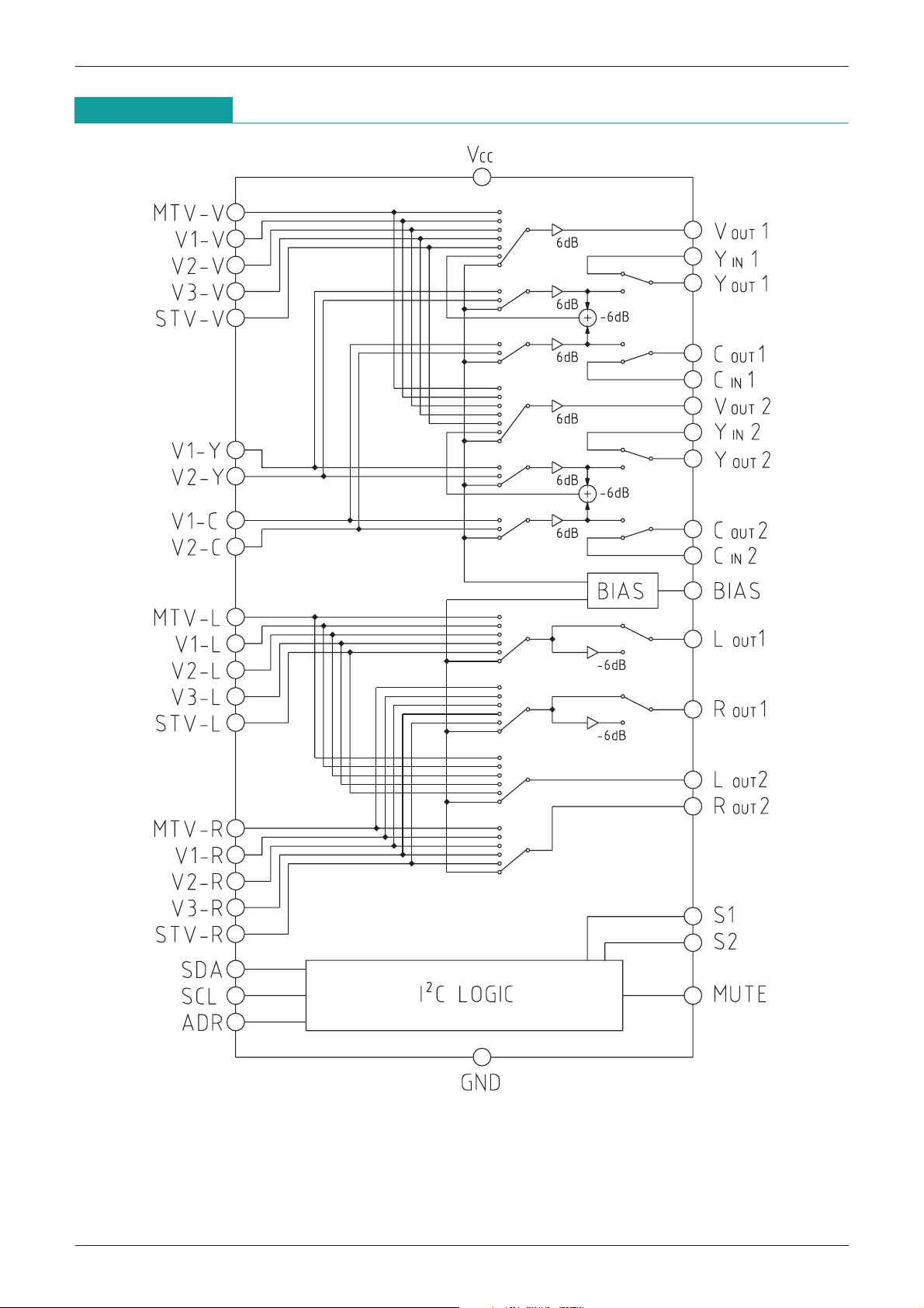
Block Diagram
2
C BUS Controlled 5-Input 2-Output AV Switch MM1492AF
I
Page 3
2
SOP-44B
136924587
10 11
44 40 3743 41 39 38 3642 341233133214311530162917281827192620252124222335
C BUS Controlled 5-Input 2-Output AV Switch MM1492AF
MITSUMI
I
Pin Assignment
1 V1-V 12 S2 23 VOUT2 34 YIN1
2 V1
3 V1
4 V1
5 V1
6 S1 17 STV
7 V2
8 V2-L 19 YIN2 30 SCL 41 COUT1
9 V2
10 V2
11 V2
-
L 13 V3-V 24 ROUT2 35 ROUT1
-
Y 14 V3-L 25 COUT2 36 LOUT1
-
R 15 V3-R 26 LOUT2 37 VOUT1
-
C 16 STV-V 27 YOUT2 38 BIAS
-
L 28 GND 39 YOUT1
-
V 18 STV-R 29 SDA 40 VCC
-
Y 20 ADR 31 MUTE 42 MTV-R
-
R 21 CIN2 32 CIN1 43 MTV-V
-
C 22 GND 33 GND 44 MTV-L
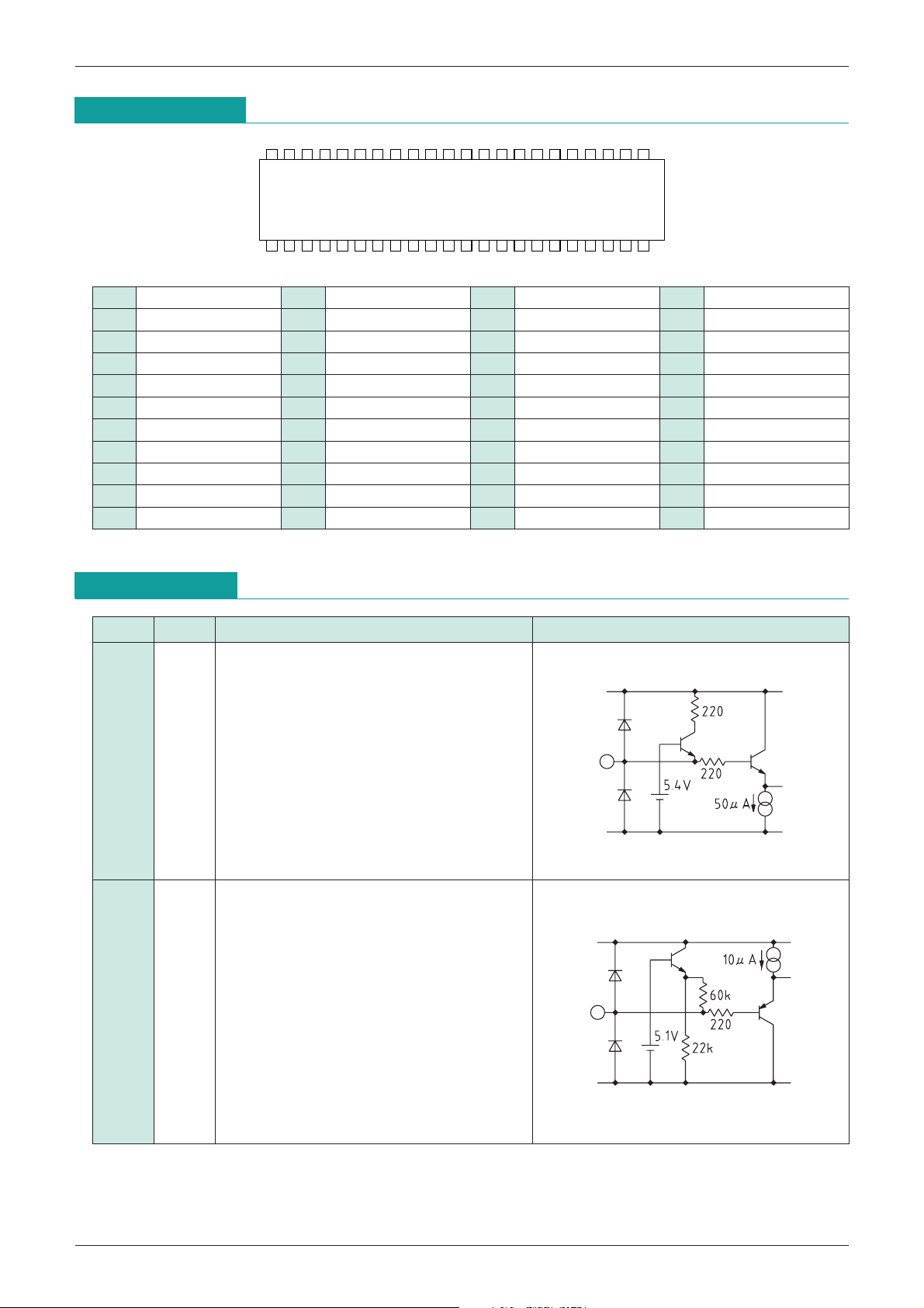
Pin Description
Pin No.
Pin name
1 V1
3 V1
7 V2
9 V2
13 V3
16 STV
19 Y
34 Y
43 MTV
2 V1
4 V1
8 V2
10 V2
14 V3
15 V3
17 STV
IN2
IN1
-
V Video input terminal
-
Y (Composite or Y)
-
V
-
Y
-
V
-
V
-
V
-
L Audio input terminal
-
R
-
L
-
R
-
L
-
R
-
L
Sync chip clamp
*
Functions Internal equivalet circuit diagram
18 STV
42 MTV
44 MTV
-
R
-
R
-
L
Page 4
MITSUMI
2
C BUS Controlled 5-Input 2-Output AV Switch MM1492AF
I
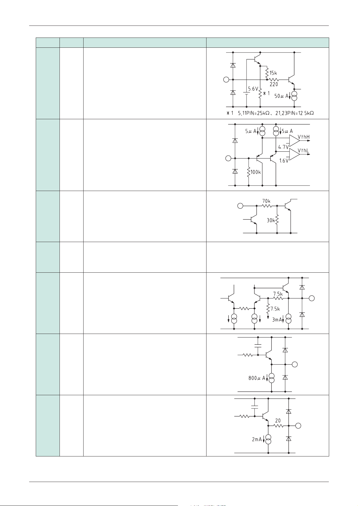
Pin No.
Pin name
5 V1
11 V2
21 C
32 C
-
C Video input terminal
-
C (Croma)
IN2
IN1
Functions Internal equivalet circuit diagram
6 S1 Distinction 3-effects input terminal
12 S2 DC Detect
20 ADR Sleve address select
31 Mute Audio Mute terminal
22 GND GND
28
33
23 V
37 V
24 R
26 L
35 R
36 L
25 C
27 Y
39 Y
41 C
OUT2 Composite video out
OUT1
OUT2 Audio out terminal
OUT2
OUT1
OUT1
OUT2S
OUT2
OUT1
OUT1
-
Video out terminal
Page 5
MITSUMI
2
C BUS Controlled 5-Input 2-Output AV Switch MM1492AF
I
Pin No.
Pin name
29 SDA Data input from I
30 SCL CLK input from I
38 BIAS Internal bias terminal
Functions Internal equivalet circuit diagram
2
C
2
C
40 V
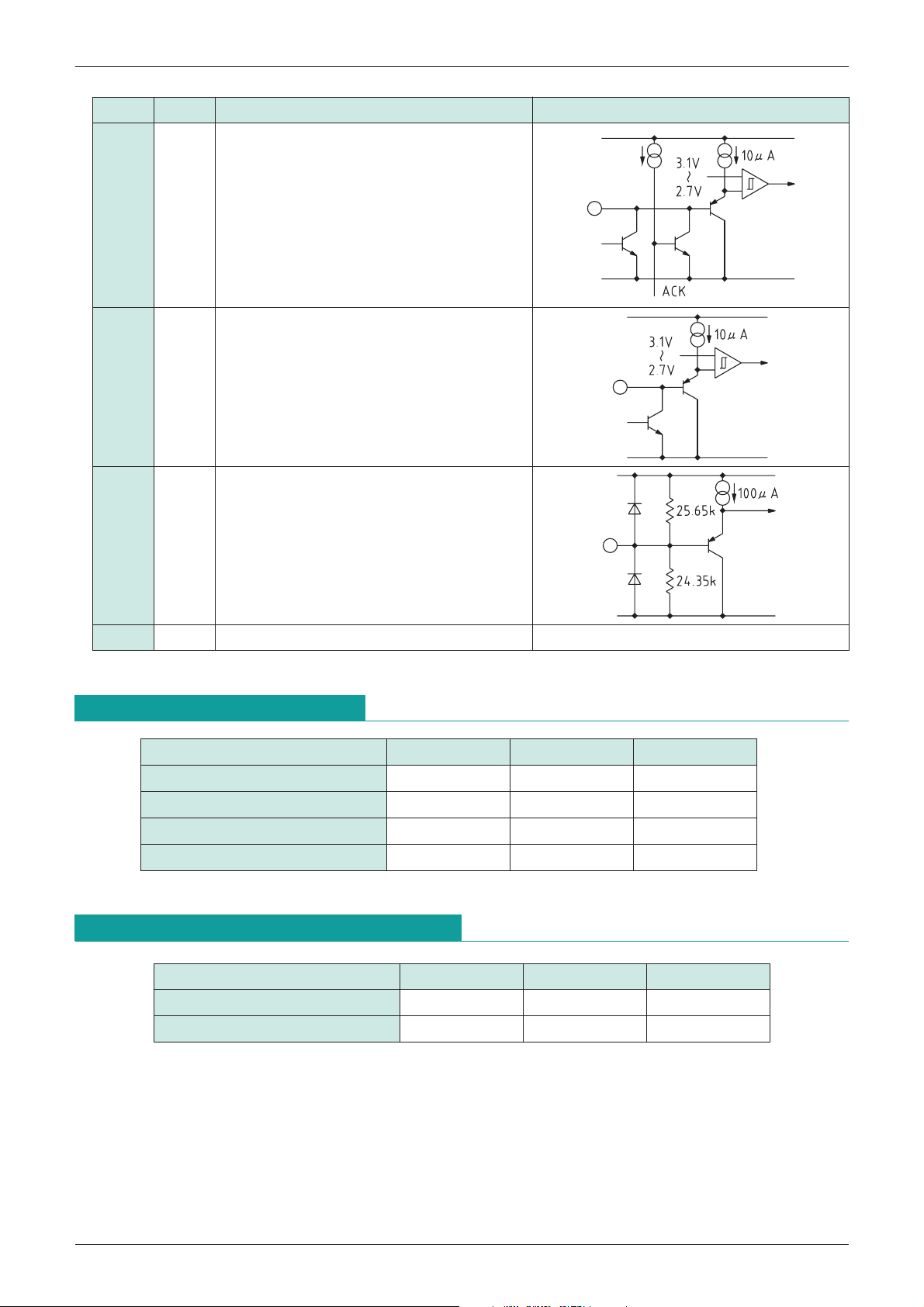
Absolute Maximum Ratings
CC VCC
(Ta=25°C)
Item Symbol Ratings Units
Storage temperature T
Operating temperature T
Power supply voltage V
STG
OPR
CCmax. 12 V
Allowable loss Pd 1100 mW
Recommended Operating Conditions
Item Symbol Ratings Units
Operating temperature T
Operating voltage V
-
40~+125 °C
-
20~+75 °C
OPR
OP +8~+10 V
-
20~+75 °C
Page 6

MITSUMI
2
C BUS Controlled 5-Input 2-Output AV Switch MM1492AF
I
Electrical Characteristics
Item Symbol Measurement conditions Min. Typ. Max. Units
Current consumption I
V
OUT1
Voltage gain G
Frequency characteristics f
Differential gain DG
Differential phase DP
Input dynamic ranges D
VOUT2
Voltage gain G
Frequency characteristics f
Differential gain DG
Differential phase DP
Input dynamic range D
YOUT1
Voltage gain
Frequency characteristics
Differential gain DG
Differential phase DP
Input dynamic range
Output impedance ZOY1 (50) Ω
Y
OUT2
Voltage gain
Frequency characteristics
Differential gain DG
Differential phase DP
Input dynamic range
Output impedance ZOY2 (50) Ω
C
OUT1
Voltage gain
Frequency characteristics
Differential gain DG
Differential phase DP
Input dynamic range
Input impedance ZIC1 Vn
Output impedance Z
(
Except where noted otherwise,
CC No signal 39 55 71 mA
V1 SIN wave : 1VP-P 100kHz 5.5 6.0 6.5 dB
V1 SIN wave : 1VP-P 10MHz/100kHz
V1 Staircase signal 1VP-P
V1 Staircase signal 1VP-P
V1 SIN wave : 100kHz THD=1.0% 1.4 1.5 VP-P
V2 SIN wave : 1VP-P 100kHz 5.5 6.0 6.5 dB
V2 SIN wave : 1VP-P 10MHz/100kHz
V2 Staircase signal 1VP-P
V2 Staircase signal 1VP-P
V2 SIN wave : 100kHz THD=1.0% 1.4 1.5 VP-P
Y1 Vn
G
G
Y2 YIN1 : SIN wave 2VP-P 100kHz
f
Y1 Vn
f
Y2 YIN1 : SIN wave 2VP-P
Y1
Y1
Y1 Vn
D
-
Y : SIN wave 1VP
-
Y : SIN wave 1VP
Vn-Y : Staircase signal 1VP
Y
IN1 : Staircase signal 2VP-P
Vn-Y : Staircase signal 1VP
Y
IN1 : Staircase signal 2VP-P
-
Y : SIN wave 100kHz THD=1.0% 1.4 1.5 VP
VCC=9V, Ta=25°C)
-
1.0 0.0 1.0 dB
-
30 3 %
-
3 0 3 deg
-
1.0 0.0 1.0 dB
-
30 3 %
-
3 0 3 deg
-
P 100kHz 5.5 6.0 6.5 dB
-
0.5 0.0 0.5 dB
-
P
-
P
-
P
-
1.0 0.0 1.0 dB
-
1.0 0.0 1.0 dB
-
30 3 %
-
30 3 %
-
3 0 3 deg
-
3 0 3 deg
DY2 YIN1 : SIN wave 100kHz THD=1.0% 3.2 3.8 VP
G
Y3 Vn
G
Y4 YIN2 : SIN wave 2VP-P 100kHz
f
Y3 Vn
Y4 YIN2 : SIN wave 2VP-P
f
Y2
Y2
D
Y3 Vn
-
Y : SIN wave 1VP
-
Y : SIN wave 1VP
Vn-Y : Staircase signal 1VP
Y
IN2 : Staircase signal 2VP-P
Vn-Y : Staircase signal 1VP
Y
IN2 : Staircase signal 2VP-P
-
Y : SIN wave 100kHz THD=1.0% 1.4 1.5 VP
-
P 100kHz 5.5 6.0 6.5 dB
-
0.5 0.0 0.5 dB
-
P
-
P
-
P
-
1.0 0.0 1.0 dB
-
1.0 0.0 1.0 dB
-
30 3 %
-
30 3 %
-
3 0 3 deg
-
3 0 3 deg
DY4 YIN2 : SIN wave 100kHz THD=1.0% 3.2 3.8 VP
C1 Vn
G
G
C2 CIN1 : SIN wave 2VP-P 100kHz
f
C1 Vn
f
C2 CIN1 : SIN wave 2VP-P
C1 CIN1 : Staircase signal 2VP-P
C1 CIN1 : Staircase signal 2VP-P
D
C1 Vn
-
C : SIN wave 1VP
-
C : SIN wave 1VP
-
Y : SIN wave 100kHz THD=1.0% 2.75 3.25 VP
-
P 100kHz 5.5 6.0 6.5 dB
-
0.5 0.0 0.5 dB
-
P
-
1.0 0.0 1.0 dB
-
1.0 0.0 1.0 dB
-
30 3 %
-
3 0 3 deg
DC2 YIN1 : SIN wave 100kHz THD=1.0% 5.5 6.5 VP
-
C and CIN1 101520kΩ
OC1 (50) Ω
-
P
-
P
-
P
-
P
-
P
-
P
Page 7

MITSUMI
Item Symbol Measurement conditions Min. Typ. Max. Units
C
OUT2
Voltage gain
Frequency characteristics
Differential gain DG
Differential phase DP
Input dynamic range
Input impedance ZIC2 CIN2 101520kΩ
Output impedance Z
L
OUT1
Voltage gain
Frequency characteristics f
Total harmonic distortion THD
Input dynamic range D
Output offset voltage V
Input impedance Z
Output impedance Z
L
OUT2
Voltage gain
Frequency characteristics f
Total harmonic distortion THD
Input dynamic range D
Output offset voltage VOFF
Output impedance Z
R
OUT1
Voltage gain
Frequency characteristic f
Total harmonic distortion THD
Input dynamic range D
Output offset voltage V
Input impedance Z
Output impedance Z
R
OUT2
Voltage gain
Frequency characteristics f
Total harmonic distortion THD
Input dynamic range D
Output offset voltage V
Output impedance Z
2
C BUS Controlled 5-Input 2-Output AV Switch MM1492AF
I
G
C3 Vn
G
C4 CIN2 : SIN wave 2VP-P 100kHz
C3 Vn
f
f
C4 CIN2 : SIN wave 2VP-P
C2 CIN1 : Staircase signal 2VP-P
C2 CIN2 : Staircase signal 2VP-P
D
C3 Vn
-
C : SIN wave 1VP
-
C : SIN wave 1VP
-
Y : SIN wave 100kHz THD=1.0% 2.75 3.25 VP
-
P 100kHz 5.5 6.0 6.5 dB
-
0.5 0.0 0.5 dB
-
P
-
1.0 0.0 1.0 dB
-
1.0 0.0 1.0 dB
-
30 3 %
-
3 0 3 deg
DC4 YIN2 : SIN wave 100kHz THD=1.0% 5.5 6.5 VP
OC2 (50) Ω
L1 SIN wave 2.5VP-P 1kHz
G
G
L2 SIN wave 2.5VP-P 1kHz 0dB Select
L1 SIN wave 2.5VP-P 1MHz/1kHz
L1 SIN wave 2.5VP-P 1kHz 0.03 0.1 %
L1 SIN wave 1kHz THD<0.5% 2.6 2.8 Vrms
OFFL1 DC offset at the switching time 0 ±15 mV
IL1 42 60 78 kΩ
OL1 (120) Ω
G
L3 SIN wave 2.5VP-P 1kHz
G
L4 SIN wave 2.5VP-P 1kHz 0dB Select
L2 SIN wave 2.5VP-P 1MHz/1kHz
L2 SIN wave 2.5VP-P 1kHz 0.03 0.1 %
L2 SIN wave 1kHz THD<0.5% 2.6 2.8 Vrms
L2 DC offset at the switching time 0 ±15 mV
OL2 (120) Ω
G
R1 SIN wave 2.5VP-P 1kHz
G
R2 SIN wave 2.5VP-P 1kHz 0dB Select
R1 SIN wave 2.5VP-P 1MHz/1kHz
R1 SIN wave 2.5VP-P 1kHz 0.03 0.1 %
R1 SIN wave 1kHz THD<0.5% 2.6 2.8 Vrms
OFFR1 DC offset at the switching time 0 ±15 mV
IR1 42 60 78 kΩ
OR1 (120) Ω
G
R3 SIN wave 2.5VP-P 1kHz
G
R4 SIN wave 2.5VP-P 1kHz 0dB Select
R2 SIN wave 2.5VP-P 1MHz/1kHz
R2 SIN wave 2.5VP-P 1kHz 0.03 0.1 %
R2 SIN wave 1kHz THD<0.5% 2.6 2.8 Vrms
OFFR2 DC offset at the switching time 0 ±15 mV
OR2 (120) Ω
-
6dB Select
-
6dB Select
-
6dB Select
-
6dB Select
-
6.5-6.0-5.5 dB
-
0.5 0.0 0.5 dB
-
3.0 0.0 1.0 dB
-
6.5-6.0-5.5 dB
-
0.5 0.0 0.5 dB
-
3.0 0.0 1.0 dB
-
6.5-6.0-5.5 dB
-
0.5 0.0 0.5 dB
-
3.0 0.0 1.0 dB
-
6.5-6.0-5.5 dB
-
0.5 0.0 0.5 dB
-
3.0 0.0 1.0 dB
-
P
-
P
Page 8

MITSUMI
SDA
SCL
P S Sr P
t HD:STA
t LOW t HD:DAT
t R t F
t HIGH t SU:DAT t SU:STA t SU:STO
t BUR
Item Symbol Measurement conditions Min. Typ. Max. Units
Crosstalk (
1)
*
V
OUT1 CTV1
V
OUT2 CTV2
Y
OUT1 CTY1 SG2 : 4.43MHz 1VP-P
Y
OUT2 CTY2 SG2 : 4.43MHz 1VP-P
C
OUT1 CTC1 SG3 : 4.43MHz 1VP-P
C
OUT2 CTC2 SG3 : 4.43MHz 1VP-P
L
OUT1 CTL1 1kHz 2.5VP-P
L
OUT2 CTL2 1kHz 2.5VP-P
R
OUT1 CTR1 1kHz 2.5VP-P
R
OUT2 CTR2 1kHz 2.5VP-P
Terminal voltage
Video input terminal V
V
OUT1/2 terminal VVOP No signal, No load 3.9 4.2 4.5 V
Y
OUT1/2 terminal VYOP No signal, No load 3.2 3.5 3.8 V
C
OUT1/2 terminal VCOP No signal, No load 3.2 3.5 3.8 V
Audio input terminal V
Audio output terminal V
2
I
C condition (Refer to figure below)
Input voltage L V
Input voltage H V
Low level output voltage V
High level input current I
Low level input current I
Clock frequency f
Data transfer wait time t
SCL start hold time t
SCL low level hold time t
SCL high level hold time t
SCL start setup time t
SDA data hold time t
SDA data setup time t
SCL rise
SCL fall
-
time tR 1000 nS
-
time tF 300 nS
SCL stop setup time t
(The inside of parentheses is design guarantee value.)
VIP No signal, No load 4.6 4.9 5.2 V
AIP No signal, No load 4.0 4.3 4.6 V
AOP No signal, No load 3.9 4.2 4.5 V
IL 0.0 1.5 V
IH 3.0 5.0 V
OL SDA sink 3mA 0.0 0.4 V
IH SDA, SCL=4.5V
IL SDA, SCL=0.4V
SCL 100 kHz
BUF 4.7 µS
HD : STA 4.0 µS
LOW 4.7 µS
HIGH 4.0 µS
SU : STA 4.7 µS
HD : DAT 200 nS
SU : DAT 250 nS
SU : STO 4.0 µS
2
C BUS Controlled 5-Input 2-Output AV Switch MM1492AF
I
SG1 : 4.43MHz 1V
SG1 : 4.43MHz 1V
P-P
(At mix, SG2/3 input)
P-P
(At mix, SG2/3 input)
-
60-53 dB
-
60-53 dB
-
60-53 dB
-
60-53 dB
-
60-53 dB
-
60-53 dB
-
90-80 dB
-
90-80 dB
-
90-80 dB
-
90-80 dB
-
10 10 V
-
10 10 V
I2C condition
Page 9

MITSUMI
(Note.1) : Input signal symbol
Vn
-
V=MTV-V, V1-V, V2-V,V3-V, STV-V
Vn
-
Y=V1-Y, V2-Y
Vn
-
C=V1-C, V2-C
(Note.2) :
(Note.3) : Video inputs
1 Test Circuit of Crosstalk
*
See Test Circuit 2
Vn-V, Vn-Y, and YINn inputs are sync chip clamped, while Vn-C and CINn inputs are non-clamped.
Measuring Circuit
Measuring Circuit 1
2
C BUS Controlled 5-Input 2-Output AV Switch MM1492AF
I
Page 10

MITSUMI
Measuring Circuit 2 (Crosstalk measurement)
2
C BUS Controlled 5-Input 2-Output AV Switch MM1492AF
I
Page 11

2
SDA
SCL
S:Start Condition
P:Stop Condition
A:Acknowledge
S38A21A87654321 P
C BUS Controlled 5-Input 2-Output AV Switch MM1492AF
MITSUMI
I
I2C BUS
I2C BUS is inter bus system controled by 2 lines (SDA, SCL).
Data are transmitted and received in the units of byte and Acknowledge.
It is transmitted by MSB first from the Start conditions.
[Control registers]
Control registers are data sent from the master for determining the switch conditions.
The data format is set as shown in the following figure.
S
Slave address
1001000/10
R/W
A
Control register 1
b7 b6 b5 b4 b3 b2 b1 b0
A
Control register 2
b7 b6 b5 b4 b3 b2 b1 b0
AP
Address byte Control data
Out of the Address byte, first 7bit are assigned to the slave address, while the residual 1bit is assigned to the
R/W bit.
Set the R/W bit to 0 when data are used control registers.
As MM1492 slave address, either 90H or 92H can be selected according to the ADR terminal conditions.
When ADR terminal is L, 90H is selected.
The following figure indicates the control contents of control registers and switches.
Each bit of control registers is reset to 0, when power
-
on.
Register b7 b6 b5 b4 b3 b2 b1 b0
1 Audio Gain 1 S/Comp select 1 Video out1 select Audio out1 select
2 Audio Gain 2 S/Comp select 2 Video out2 select Audio out2 select
MM1492 consists of one address byte and two control data bytes (3bytes in total).
All data over the limited length (4th and subsequent bytes) are fully neglected.
For details of the control contents of switches, refer to the separate table.
Page 12

MITSUMI
Reset
off
Reset
on
4.3V 5.4V
V
CC
[Status registers]
Status registers are data to inform the device status.
The data format is set as shown in the following figure.
2
C BUS Controlled 5-Input 2-Output AV Switch MM1492AF
I
S
A
Slave address R/W
Status register
NA P
1 0 0 1 0 00/11 b7b6b5b4b3b2b1b0
Address byte device status
Out of the Address byte, first 7bit are assigned to the slave address, while the residual 1bit is assigned to the
R/W bit.
Set the R/W bit to 1 when data are used status registers.
As MM1492 slave address, either 91H or 93H can be selected according to the ADR terminal conditions.
When ADR terminal is L, 91H is selected.
Set the confirmation acknowledgement after the end of status register to non
-
acknowledgement.
The following figure shows the correspondence of the output data of status registers.
b7 b6 b5 b4 b3 b2 b1 b0
P-ON S1 S1 S2 S2
RESET
OPEN SEL OPEN SEL
P-on RESET : 1 returns when the power on reset is done, 0 returns after reading data once.
S1/S2 OPEN : S1/S2 OPEN and SEL are identified by 3 values, and output according to the
S1/S2 SEL combinations in the following table.
DC voltage of S1/S2 S1/S2 OPEN S1/S2 SEL
<
0.8V
DC 01
=
<
1.3V
<
DC
3.5V 00
=
=
<
DC
4.5V 10
=
[about power on reset]
MM1492 is provided with a power on reset function to reset each control register to 0 when power supply is
turned on.
The power on reset threshold has the hysteresis as shown in following figure.
Page 13

MITSUMI
Switch Control Table
(1) Video output 1
b6 b5 b4 b3 VOUT1YOUT1COUT1
0 0 0 0 Mute Mute Mute
2
C BUS Controlled 5-Input 2-Output AV Switch MM1492AF
I
0001 MTV
0010 V1
0011 V2
0100 V3
0101 STV
0110
0111
1 0 0 0 Mute Mute Mute
1001 MTV
1010 V1
1011 V2
1100 V3
1101 STV
1110
1111
(2) Audio output 1
-
VYIN1CIN1
-
VYIN1CIN1
-
VYIN1CIN1
-
VYIN1CIN1
-
VYIN1CIN1
Mute Mute Mute
-
VYIN1CIN1
-
(Y+C) V1-YV1
-
(Y+C) V2-YV2
-
VYIN1CIN1
-
VYIN1CIN1
Mute Mute Mute
Mute terminal b2 b1 b0 LOUT1ROUT1
0 0 0 Mute Mute
-
C
-
C
(3) Audio gain
0 0 1 MTV
010 V1
<
1.5V (OPEN)
=
>
3.0V Mute Mute
=
011 V2
100 V3
101 STV
110
111
b7 LOUT1ROUT1
0
1 0dB 0dB
-
6dB
-
L MTV-R
-
LV1
-
LV2
-
LV3
-
LSTV
Mute Mute
-
6dB
-
R
-
R
-
R
-
R
Page 14

MITSUMI
Application Circuit
2
C BUS Controlled 5-Input 2-Output AV Switch MM1492AF
I
Note.
(1) V
OUT is set to 4.2V, While CIN is set to 4.9V.
Be careful since the capacity polarity may differ according to the comb filter bias.
(2) Each audio output can be set to myte by setting pin 31 to high. The mute is turned off in when pin 19 is
open or low.
 Loading...