

Page 1
MM145453
Liquid Crystal Display Driver
MM145453 Liquid Crystal Display Driver
December 1999
General Description
The MM145453 is a monolithic integrated circuit utilizing
CMOS metal gate, low threshold enhancement mode devices. The chip can drive up to 33LCDsegmentsand can be
paralleled to increase this number. The chip is capable of
driving a 4
between the display and the data source.
The MM145453 stores display data in latches after it is
clocked in, and holds the data until new display data is received.
The MM145453 is available in a molded 44 pin surface
mount PLCC package. The MM145453 is pin out and functionally compatible with the MC145453.
1
⁄2digit 7-segment display with minimal interface
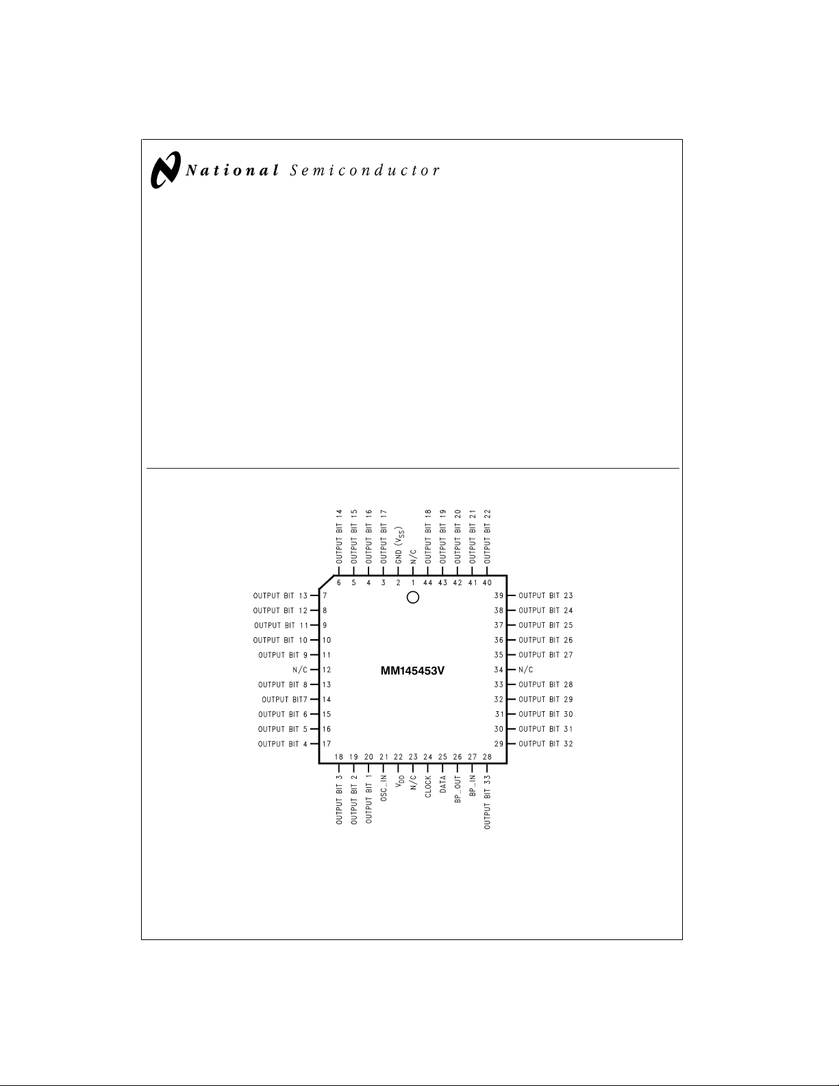
Connection Diagram
Features
n Serial Data Input
n Wide Power Supply operation
n TTL Compatibility
n Up to 33 LCD Segments
n Alphanumeric or Bar Graph capability
n Cascaded operation capability
n Pin Compatible with MC145453
Applications
n COPS™or microprocessor displays
n Industrial control indicator
n Digital clock, thermometer, counter, voltmeter
n Instrumentation displays
n Remote displays
DS101283-1
Top View
Order Number MM145453V
See NS Package Number V44A
© 1999 National Semiconductor Corporation DS101283 www.national.com
Page 2
Absolute Maximum Ratings (Note 1)
If Military/Aerospace specified devices are required,
please contact the National Semiconductor Sales Office/
MM145453
Distributors for availability and specifications.
Voltage at Any Pin,
Referenced to Gnd
Storage Temperature -65˚C to +150˚C
Power Dissipation at 25˚C 350mW
Power Dissipation at 70˚C 300mW
-0.3V to +10V
Junction Temperature +150˚C
Lead Temperature
300˚C
(Soldering, 10s)
Recommended Operating
Conditions
V
DD
Operating Temperature 0˚C to 70˚C
3V to 10V
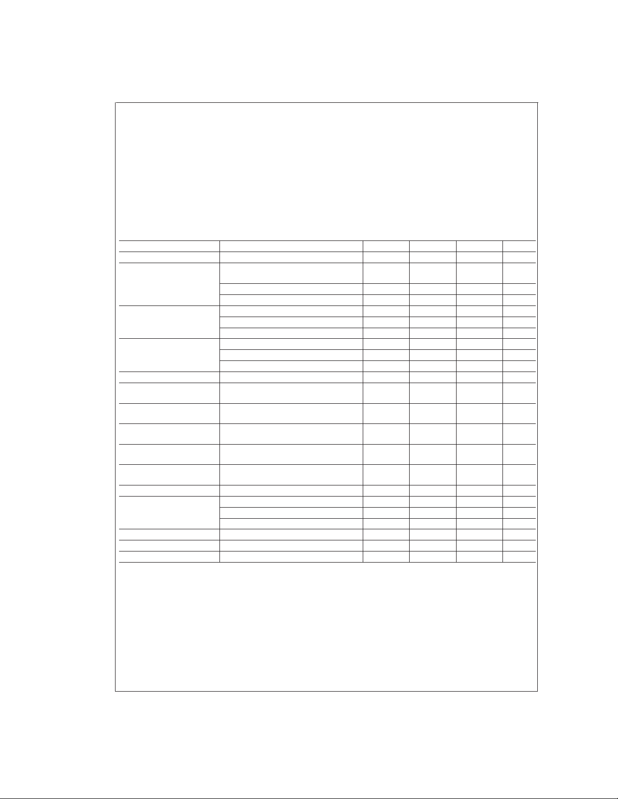
Electrical Characteristics
The following specifications apply for TAwithin operation range, V
=
3.0V to 10V, V
DD
Parameter Conditions Min Typical Max Units
Supply Voltage, V
Average Supply Current, I
Input Logical ’0’ Voltage, V
Input Logical ’1’ Voltage, V
Segment Sink Current, I
Segment Source Current,
I
OH
Backplane Out Sink Current,
I
OL
Backplane Out Source
Current, I
Segment Output Offset
DD
OH
All Outputs Open, Clock=Gnd,
DD
Data=Gnd,OSC=Gnd, BP_IN 32Hz
=5V 10 µA
V
DD
V
= 10V 40 µA
DD
ILVDD
IHVDD
OL
= 3V 0.4 V
V
= 5V 0.8 V
DD
V
= 10V 0.8 V
DD
= 3V 2.0 V
V
= 5V 2.0 V
DD
V
= 10V 8.0 V
DD
VDD= 3V, V
VDD= 3V, V
VDD= 3V, V
VDD= 3V, V
= 0.3V -20 -40 µA
OUT
= 2.7V
OUT
= 0.3V
OUT
= 2.7V
OUT
Segment Load = 250pF (Note 2)
Voltage
Backplane Output Offset
Backplane Load = 8750pF (Note 2)
Voltage
Backplane Out Frequency R
Clock Input Frequency,
f
CLOCK
= 50kΩ,C
OSC_IN
VDD= 3V (Notes 2, 3) 500 kHz
V
= 5V (Note 2) 750 kHz
DD
V
= 10V (Note 2) 1.0 MHz
DD
= 0.01µF 75 Hz
OSC_IN
Clock Input Duty Cycle 40 60
Data Input Set-Up Time, t
Data Input Hold Time, t
Note 1: “Absolute Maximum Ratings” are those values beyond which the safety of the device cannot be guaranteed. They are not meant to imply that the devices
should be operated at these limits. The table of “Electrical Characteristics” specifies conditions of device operation.
Note 2: This parameter is guaranteed (but not production tested) over the operating temperature range and the operating supply voltage range. Not to be used in
Q.A. testing.
Note 3: AC input waveform for test purposes: t
Note 4: Clock input rise time (t
DS
DH
≤ 20ns, tf≤ 20ns, f
) and fall time (tf) must not exceed 300ns
r
r
=
500kHz, Duty Cycle = 50
CLOCK
%
=
0V, unless otherwise specified.
SS
310V
20 40 µA
-320 -500 µA
320 500 µA
+/-50 mV
+/-50 mV
300 ns
300 ns
±
%
10
%
www.national.com 2
Page 3

Electrical Characteristics (Continued)
Block Diagram
MM145453
DS101283-2
FIGURE 1.
Applications Information
The MM145453 is specifically designed to operate 41⁄2digit
7-segment displays with minimal interface with the display
and data source. Serial data transfer from the data source to
the display driver is accomplished with 2 signals, serial Data
and Clock. Using a format of a leading ″1″ followed by the 33
data bits and 2 trailing don’t care bits, allows data transfer
without the need of an additional Data Load signal. Since the
MM145453 does not contain a character generator, the formatting of the segment information must be done prior to inputting the data to the MM145453. The transfer of the 33
data bits is complete at the falling edge of the 36th clock
cycle, thus providing non-multiplexed, direct drive to the display. Outputs change only if the serial data bits differ from
the previous time.
Figure 3
shows the data input format. Asinglestartbit of logical ’1’ precedes the 33 bits of segment data for a total of 34
bits that need to be defined and clocked in. After the 34 bits
are clocked in, 2 additional clock cycles are required. At the
36th clock cycle an internal LOAD signal is generated synchronously with the rising edge of the Clock In signal, which
loads the 33 bits of segment data in the shift register into the
latches.At the falling edge of the 36th clock cycle an internal
RESET signal is generated which clears all the shift registers
for the next set of data. The shift registers are static masterslave configuration. There is no clear for the master portion
DS101283-3
FIGURE 2.
of the first shift register, thus allowing continuous operation.
The data during the 35th and 36th clock cycles is ″don’t
care″, but setting data to logical ’0’ for these two clock cycles
is the preferred format.
The data input bits map directly to the segment output pins
and the display. The MM145453 does not have any format
restrictions, as all outputs are controllable.
The MM145453 has an internal oscillator which can generate the required clock signal to drive the LCD back plane.
The frequency of the internal oscillator is set by a pull-up resistor (R
a capacitor (C
Ground. Due to the current sink limitations of the OSC_IN
) connected from the OSC_IN pin to VDD, and
OSC_IN
) connected from the OSC_IN pin to
OSC_IN
circuitry, the lowest recommended resistor value for setting
the oscillator frequency is 9kΩ. It will typically take 2 to 4 RC
time constants to charge the OSC_IN pin from near 0V to
within 1V of V
the OSC_IN circuitry.An approximate calculation of f
=1/(lη(VDD/1V) X R
f
OSC
AR
OSC_IN
value of 0.01µF and a V
typical oscillator frequency ( f
f
signal is divided by 16 before it is presented at the
OSC
BP_OUT pin. For this example the approximate BP_OUT
frequency will be f
which is the high threshold voltage point for
DD
OSC_INXCOSC_IN
resistor value of 50kΩ with a C
value of 5.00V would produce a
DD
/16, or about 75Hz.
OSC
) of about 1200Hz. The
OSC
)
OSC_IN
capacitor
www.national.com3
OSC
is:
Page 4

Applications Information (Continued)
The BP_IN pin of the MM145453 can be used with an externally supplied signal, provided it has a duty cycle of 50%.
MM145453
Any deviation from a precise 50%duty cycle will result in an
offset voltage on the LCD. The use of an external clock allows synchronizing the display drive with AC power,other internal clocks, or DVM integration time to reduce interference
Input Data Format
from the display. When using an external clock for the back
plane drive the internal oscillator should be disabled by connecting the OSC_IN pin directly to ground. This will prevent
possible internal oscillations, and reduce device dissipation.
The MM145453 is a pin out variation of the MM5453. For additional applications information please refer to the MM5453
data sheet.
DS101283-4
www.national.com 4
Page 5

Physical Dimensions inches (millimeters) unless otherwise noted
MM145453 Liquid Crystal Display Driver
Order Number MM145453V
Top View
See NS Package Number V44A
LIFE SUPPORT POLICY
NATIONAL’S PRODUCTS ARE NOT AUTHORIZED FOR USE AS CRITICAL COMPONENTS IN LIFE SUPPORT
DEVICES OR SYSTEMS WITHOUT THE EXPRESS WRITTEN APPROVAL OF THE PRESIDENT AND GENERAL
COUNSEL OF NATIONAL SEMICONDUCTOR CORPORATION. As used herein:
1. Life support devices or systems are devices or
systems which, (a) are intended for surgical implant
into the body, or (b) support or sustain life, and
whose failure to perform when properly used in
accordance with instructions for use provided in the
2. A critical component is any component of a life
support device or system whose failure to perform
can be reasonably expected to cause the failure of
the life support device or system, or to affect its
safety or effectiveness.
labeling, can be reasonably expected to result in a
significant injury to the user.
National Semiconductor
Corporation
Americas
Tel: 1-800-272-9959
Fax: 1-800-737-7018
Email: support@nsc.com
www.national.com
National Semiconductor
Europe
Fax: +49 (0) 1 80-530 85 86
Email: europe.support@nsc.com
Deutsch Tel: +49 (0) 1 80-530 85 85
English Tel: +49 (0) 1 80-532 78 32
Français Tel: +49 (0) 1 80-532 93 58
Italiano Tel: +49 (0) 1 80-534 16 80
National Semiconductor
Asia Pacific Customer
Response Group
Tel: 65-2544466
Fax: 65-2504466
Email: sea.support@nsc.com
National Semiconductor
Japan Ltd.
Tel: 81-3-5639-7560
Fax: 81-3-5639-7507
National does not assume any responsibility for use of any circuitry described, no circuit patent licenses are implied and National reserves the right at any time without notice to change said circuitry and specifications.
 Loading...