

Page 1
MITSUMI
Composite Regulator MM1448
Composite Regulator
Monolithic IC MM1448
Outline
This IC was developed as a composite power supply for the RF section of mobile telephones. It is composed
of three normal voltage regulator circuits, of which the output of one circuit is divided for two switching
circuits.
The regulator output voltage is fixed, and each can be set between 2.0V and 5.0V according to the
customer's needs. Output noise voltage noise reduction is made possible by using the noise reduction pin.
Also, switch pins are provided to control each output, making this an ideal IC for use in portable equipment.
Features
1. Input/output voltage difference Vo1 : 0.2V max. Vo2 : 0.2V max. Vo3 : 0.3V max.
2. Output noise voltage Vo1 : 30µVrms typ. Vo2 : 30µVrms typ. Vo3 : 30µVrms typ.
3. Output voltage precision Vo1, Vo2, Vo3 : ±3%
4. No-load input current Vo1 : 170µA typ. Vo2 : 170µA typ. Vo3 : 170µA typ.
5. Input voltage 12V max.
6. Output current
7. Output ON/OFF control High : ON, Low : OFF
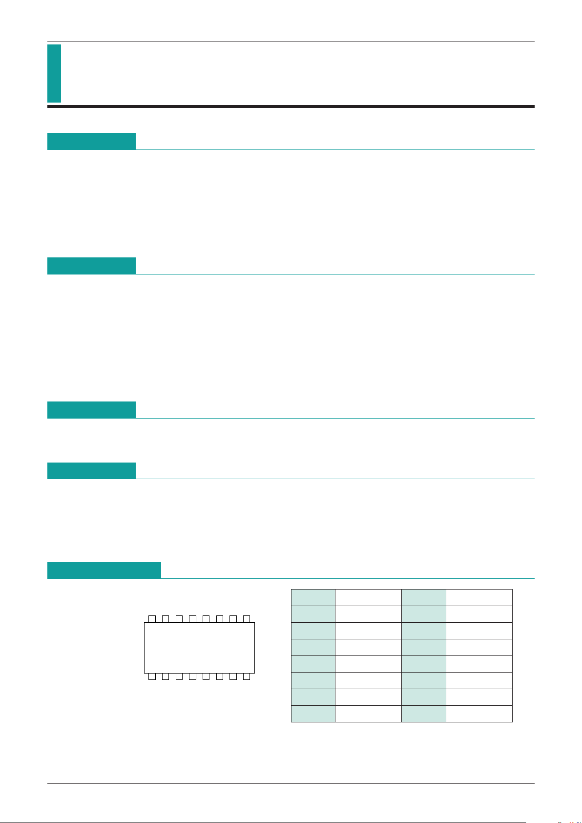
Package
VSOP-16
Applications
Pin Assignment
1. Mobile telephones, PHS
2. Video cameras
3. Portable communication equipment
4. Battery-powered portable equipment
VSOP-16
13 762458
16 13 1115 14 12910
MITSUMI
1 VO1 9 VO2
2 NS1 10 GND
3 PS1 11 PS4
4 V
IN 12 VO4
5 PS3 13 NC
6 NS3 14 V
O5
7 PS2 15 PS5
8 NS2 16 V
O3
Page 2
MITSUMI
Composite Regulator MM1448
MITSUMI
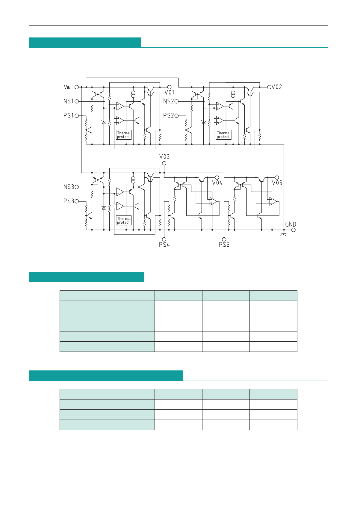
Equivalent Circuit Diagram
Absolute Maximum Ratings
Item Symbol Rating Unit
Storage Temperature T
STG
-
40~+125 °C
Operating Temperature T
OPR
-
20~+75 °C
Power Supply Voltage V
IN
-
0.3~+12 V
Output Current (1 circuit) I
O (n) 200 mA
Power Consumption Pd 400 (IC only) mW
Recommended Operating Conditions
Item Symbol Rating Unit
Operating Temperature T
OP
-
20~75 °C
Operating Voltage V
OP 1.8~12 V
Regulator Output Current (1 circuit)
IO (n) 0~100 mA
Page 3

MITSUMI
Composite Regulator MM1448
MITSUMI
Electrical Characteristics
(Except where noted otherwise, Ta=25°C, VIN=4V, CIN=10µF, C
VO (n)
=4.7µF+1Ω, C
ns (n)
=0.01µF)
Item Symbol Measurement conditions Min. Typ. Max. Unit
Standby current Iins V
PS1=VPS2=VPS3=0V 0 3 µA
No-load (unload)
Operating currents 1~3
I
IN1~3
V
PS1=3V, VPS2=VPS3=VPS4~VPS5=0V
170 350 µA
(for 1 circuit; all
V
PS2=3V, VPS1=VPS3=VPS4~VPS5=0V
3 circuits the same)
V
PS3=3V, VPS1=VPS2=VPS4~VPS5=0V
V
O1
Output voltage V
O1 Io1=30mA 2.72 2.80 2.88 V
Minimum input/
output voltage difference
Vdmin1 V
IN=2.6V, Io1=30mA 0.20 V
Load fluctuation VLo1 Io1=0~100mA 60 mV
Input fluctuation VLi1 V
IN=4.0~8.0V, Io1=30mA 20 mV
Output voltage
temperature coefficient
VO1/ T
Tj=-20~75°C, IO1=30mA ±100
ppm/°C
Ripple rejection rate RR1 f=120Hz, VRIPPLE=1VP-P, Io1=30mA 50 60 dB
Output noise voltage Vn1
f=10Hz~10kHz, Io1=30mA, Cns1=0.01µF
30 60
µVrms
Output rise time TdH1 Io1=30mA, VPS1=0 4V 0.04 0.8 mS
V
O2
Output voltage V
O2 Io2=30mA 2.72 2.80 2.88 V
Minimum input/
output voltage difference
Vdmin2 V
IN=2.6V, Io2=30mA 0.20 V
Load fluctuation VLo2 Io2=0~100mA 60 mV
Input fluctuation VLi2 V
IN=4.0~8.0V, IO2=30mA 20 mV
Output voltage
temperature coefficient
VO2/ T
Tj=-20~75°C, IO2=30mA ±100
ppm/°C
Ripple rejection rate RR2 f=120Hz, VRIPPLE=1VP-P, Io2=30mA 50 60 dB
Output noise voltage Vn2
f=10Hz~10kHz, Io2=30mA, Cns2=0.01µF
30 60
µVrms
Output rise time TdH2 Io2=30mA, VPS2=0 4V 0.04 0.8 mS
V
O3
Output voltage V
O3 Io3=30mA 2.92 3.00 3.08 V
Minimum input/
output voltage difference
Vdmin3 V
IN=2.8V, Io3=30mA 0.20 V
Load fluctuation VLo3 Io3=0~100mA 60 mV
Input fluctuation VLi3 V
IN=4.0~8.0V, IO3=30mA 20 mV
Output voltage
temperature coefficient
VO3/ T
Tj=-20~75°C, IO3=30mA ±100
ppm/°C
Ripple rejection rate RR3 f=120Hz, VRIPPLE=1VP-P, Io3=30mA 50 60 dB
Output noise voltage Vn3
f=10Hz~10kHz, Io3=30mA, Cns3=0.01µF
30 60
µVrms
Output rise time TdH3 Io3=30mA, VPS3=0 4V 0.04 0.8 mS
V
O4
Output voltage V
O4 Io3=Io4=20mA, Io5=40mA 2.82 VO3V
Output current I
O4VO4=2.72V, Io3=Io5=0mA 50 mA
Output rise time TdH4 Io4=20mA, C
VO4=1µF, VPS4=0 4V 0.02 0.1 mS
Reactive current Iq4 I
O4=20mA, VO3=3V 0.5 0.8 mA
V
O5
Output voltage V
O5 Io3=Io4=20mA, Io5=40mA 2.82 VO3V
Output current capacity I
O5VO5=2.72V, Io3=Io4=0mA 80 mA
Output rise time TdH5 Io5=40mA, C
OUT5=1µF, VPS5=0 4V 0.02 0.1 mS
Reactive current Iq5 I
O5=40mA, VO3=3V 2 2.8 mA
PS output control pin
Psn pin OFF voltage V
OFF 0.4 V
Psn pin ON voltage V
ON 1.6 V
Psn pin inflow current I
PSnVPSn=1.6V 10 µA
Page 4

MITSUMI
Composite Regulator MM1448
MITSUMI
1. Output capacitance definitely is required to perform regulator and switch phase compensation. Also,
please note that oscillation may occur depending on the ESR value.
2. Vo pin output noise voltage is reduced using NS pin capacitance value. Even if there is no need to take
output noise voltage into consideration, connection of a capacitor is recommended for stable operation and
improvement of AC characteristics.
Measurement Circuit
Input-Output Differential Voltage Line regulation
250
200
150
100
50
0
0 50 100 150
Output current (mA)
Input-Output
Differential Voltage (mV)
20
10
0
-
10
-
20
4681012
VIN (V)
Line regulation (mV)
Characteristics
Page 5

MITSUMI
Composite Regulator MM1448
MITSUMI
Output current Output capacitance (IOUT-ESR)
4
3
1
2
0
0 100 200 300
Output current (mA)
Output voltage (V)
IOUT (mA)
ESR (Ω)
1000
100
1
0.1
10
0.01
0.01 0.1 1 10 100
Area of stable operation (Stable Region)
IO4 (5) -VO34 (35)(VO3=3V)
IO (A)
5.00E-01
4.00E-01
3.00E-01
2.00E-01
1.00E-01
0.00E+00
0 0.02 0.04 0.06 0.08 0.1
VO (V)
VO4
V
O5
IO4 (5)
-
Iq4 (5)(VO3=3V)
IO (A)
6.00E-03
5.00E-03
4.00E-03
3.00E-03
2.00E-03
1.00E-03
0.00E+00
0 0.02 0.04 0.06 0.08 0.1
Iq (A)
VO4
V
O5
Load regulation Thermal shutdown
60
40
20
0
-
40
-
20
-
60
0 50 100
Output current (mA)
Load regulation (mV)
4
3
1
2
0
0 50 100 150 200
Temperature (°C)
Output voltage (V)
 Loading...