

Page 1
MIC4423/4424/4425 Micrel
MIC4423/4424/4425
Dual 3A-Peak Low-Side MOSFET Driver
Bipolar/CMOS/DMOS Process
General Description
The MIC4423/4424/4425 family are highly reliable BiCMOS/
DMOS buffer/driver/MOSFET drivers. They are higher output
current versions of the MIC4426/4427/4428, which are
improved versions of the MIC426/427/428. All three families
are pin-compatible. The MIC4423/4424/4425 drivers are
capable of giving reliable service in more demanding electrical
environments than their predecessors. They will not latch
under any conditions within their power and voltage ratings.
They can survive up to 5V of noise spiking, of either polarity,
on the ground pin. They can accept, without either damage or
logic upset, up to half an amp of reverse current (either
polarity) forced back into their outputs.
The MIC4423/4424/4425 series drivers are easier to use,
more flexible in operation, and more forgiving than other
CMOS or bipolar drivers currently available. Their BiCMOS/
DMOS construction dissipates minimum power and provides
rail-to-rail voltage swings.
Primarily intended for driving power MOSFETs, the MIC4423/
4424/4425 drivers are suitable for driving other loads
(capacitive, resistive, or inductive) which require lowimpedance, high peak currents, and fast switching times.
Heavily loaded clock lines, coaxial cables, or piezoelectric
transducers are some examples. The only known limitation on
loading is that total power dissipated in the driver must be kept
within the maximum power dissipation limits of the package.
Features
• Reliable, low-power bipolar/CMOS/DMOS construction
• Latch-up protected to >500mA reverse current
• Logic input withstands swing to –5V
• High 3A-peak output current
• Wide 4.5V to 18V operating range
• Drives 1800pF capacitance in 25ns
• Short <40ns typical delay time
• Delay times consistent with in supply voltage change
• Matched rise and fall times
• TTL logic input independent of supply voltage
• Low equivalent 6pF input capacitance
• Low supply current
3.5mA with logic-1 input
350µA with logic-0 input
• Low 3.5Ω typical output impedance
• Output voltage swings within 25mV of ground or VS.
• ‘426/7/8-, ‘1426/7/8-, ‘4426/7/8-compatible pinout
• Inverting, noninverting, and differential configurations
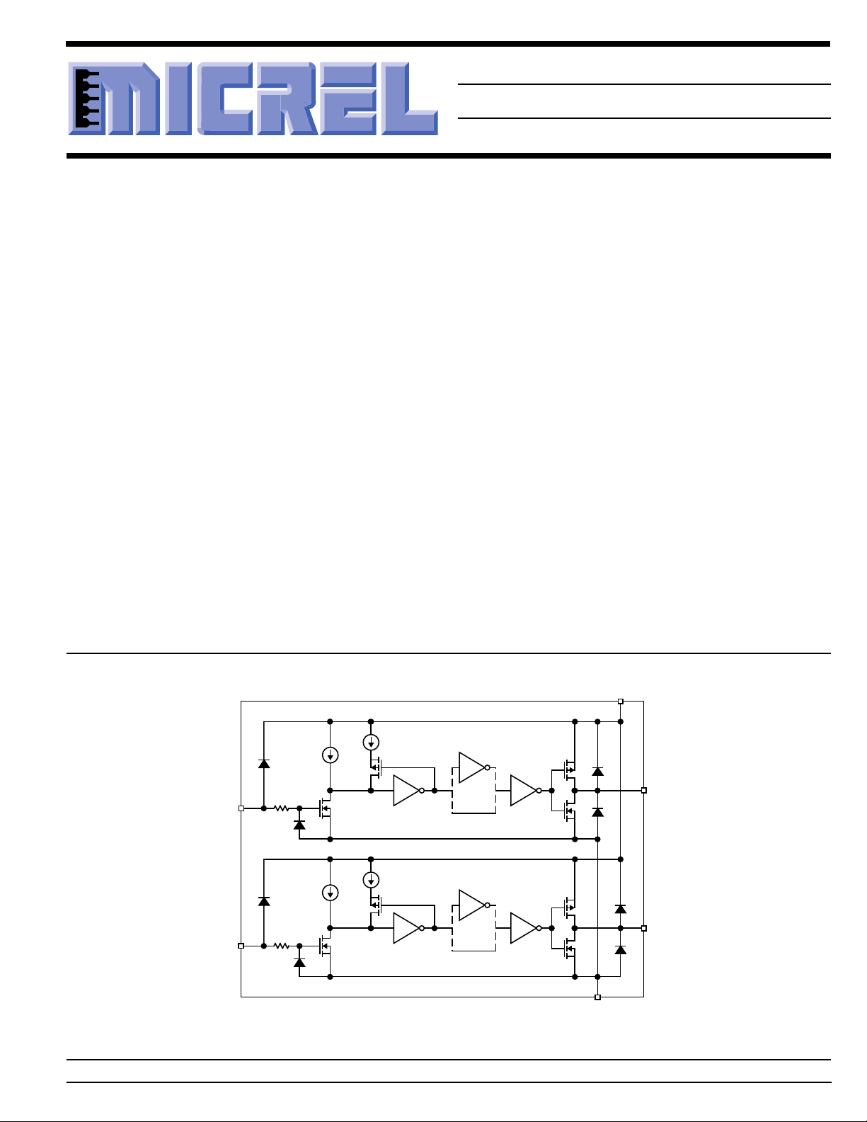
Functional Diagram
V
S
Integrated Component Count:
4 Resistors
INVERTING
NONINVERTING
INVERTING
NONINVERTING
GND
INA
INB
0.1mA
0.6mA
2kΩ
0.6mA
0.1mA
2kΩ
Ground Unused Inputs
Micrel, Inc. • 1849 Fortune Drive • San Jose, CA 95131 • USA • tel + 1 (408) 944-0800 • fax + 1 (408) 944-0970 • http://www.micrel.com
January 1999 1 MIC4423/4424/4425
4 Capacitors
52 Transistors
OUTA
OUTB
Page 2
MIC4423/4424/4425 Micrel
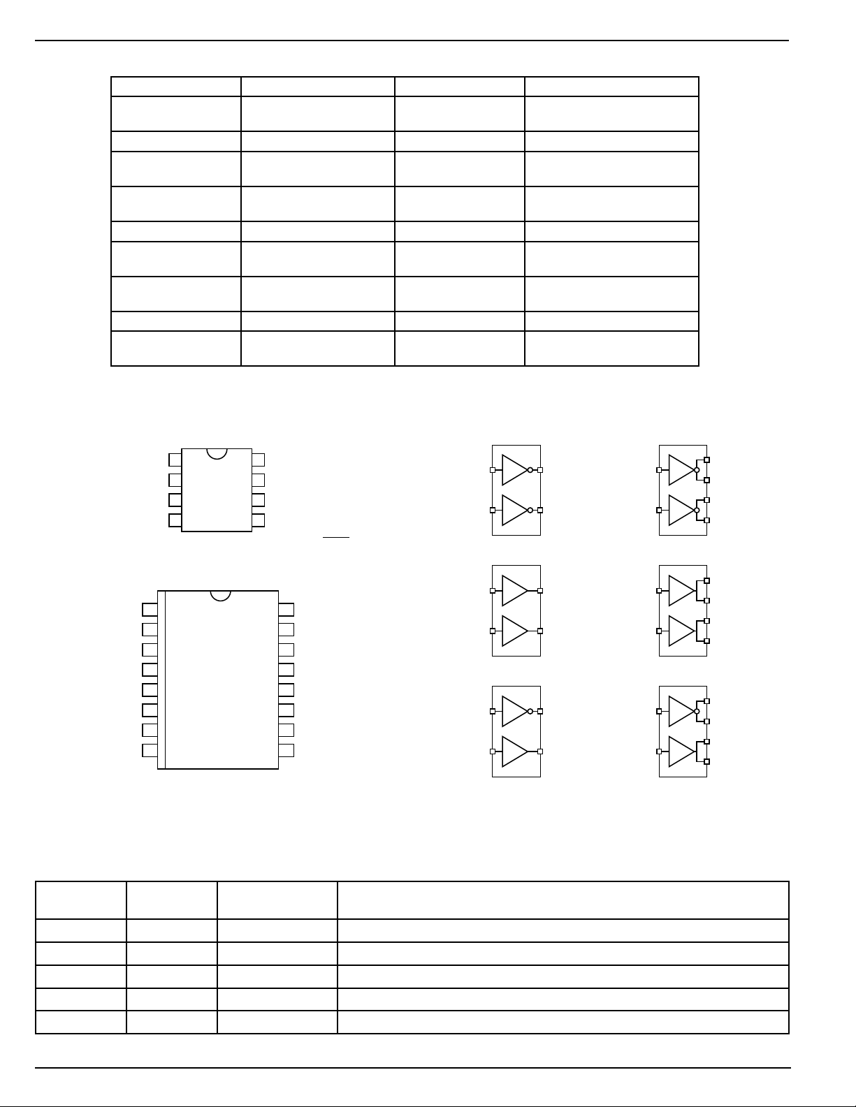
Ordering Information
Part Number Temperature Range Package Configuration
MIC4423CWM 0°C to +70°C 16-Pin Wide SOIC Dual Inverting
MIC4423BWM –40°C to +85°C
MIC4423BM –40°C to +85°C 8-Pin SOIC Dual Inverting
MIC4423CN 0°C to +70°C 8-Pin Plastic DIP Dual Inverting
MIC4423BN –40°C to +85°C
MIC4424CWM 0°C to +70°C 16-Pin Wide SOIC Dual Non-Inverting
MIC4424BWM –40°C to +85°C
MIC4424BM –40°C to +85°C 8-Pin SOIC Dual Non-Inverting
MIC4424CN 0°C to +70°C 8-Pin Plastic DIP Dual Non-Inverting
MIC4424BN –40°C to +85°C
MIC4425CWM 0°C to +70°C 16-Pin Wide SOIC Inverting + Non Inverting
MIC4425BWM –40°C to +85°C
MIC4425BM –40°C to +85°C 8-Pin SOIC Inverting + Non Inverting
MIC4425CN 0°C to +70°C 8-Pin Plastic DIP Inverting + Non Inverting
MIC4425BN –40°C to +85°C
Pin Configuration
NC
1
INA
2
GND
3
INB
4
8-pin SOIC (M)
1NC
2INA
8NC
16-lead Wide SOIC (WM)
8-pin DIP (N)
8
7
6
5
NC
OUTA
VS
OUTB
WM Package Note:
Duplicate
OUTA
, and
must be externally
connected together.
NC16
OUTA15
OUTA143NC
VS134GND
VS125GND
OUTB116NC
OUTB107INB
NC9
GND, VS
OUTB
Driver Configuration
MIC4423xN/M
A
7 OUTA
B
5 OUTB
A
7 OUTA
B
5 OUTB
A
7 OUTA
B
5 OUTB
,
pins
INA 2
INB 4
MIC4424xN/M
INA 2
INB 4
MIC4425xN/M
INA 2
INB 4
MIC4423xWM
INA 2
INB 7
MIC4424xWM
INA 2
INB 7
MIC4425xWM
INA 2
INB 7
14 OUTA
A
15 OUTA
10 OUTB
B
11 OUTB
14 OUTA
A
15 OUTA
10 OUTB
B
11 OUTB
14 OUTA
A
15 OUTA
10 OUTB
B
11 OUTB
Pin Description
Pin Number Pin Number Pin Name Pin Function
DIP, SOIC Wide SOIC
2 / 4 2 / 7 INA/B Control Input
3 4, 5 GND Ground: Duplicate pins must be externally connected together.
6 12, 13 V
S
7 / 5 14, 15 / 10, 11 OUTA/B Output: Duplicate pins must be externally connected together.
1, 8 1, 3, 6, 8, 9, 16 NC not connected
MIC4423/4424/4425 2 January 1999
Supply Input: Duplicate pins must be externally connected together.
Page 3
MIC4423/4424/4425 Micrel
Absolute Maximum Ratings (Note 1)
Supply Voltage ...........................................................+22V
Input Voltage ................................. VS + 0.3V to GND – 5V
Junction Temperature .............................................. 150°C
Storage Temperature Range .................... –65°C to 150°C
Lead Temperature (10 sec.)..................................... 300°C
ESD Susceptability, Note 3...................................... 1000V
Operating Ratings (Note 2)
Supply Voltage (VS) .................................... +4.5V to +18V
Temperature Range
C Version .................................................. 0°C to +70°C
B Version............................................... –40°C to +85°C
Package Thermal Resistance
DIP θJA............................................................. 130°C/W
DIP θJC............................................................... 42°C/W
Wide-SOIC θJA................................................. 120°C/W
Wide-SOIC θJC................................................... 75°C/W
SOIC θJA.......................................................... 120°C/W
SOIC θJC............................................................ 75°C/W
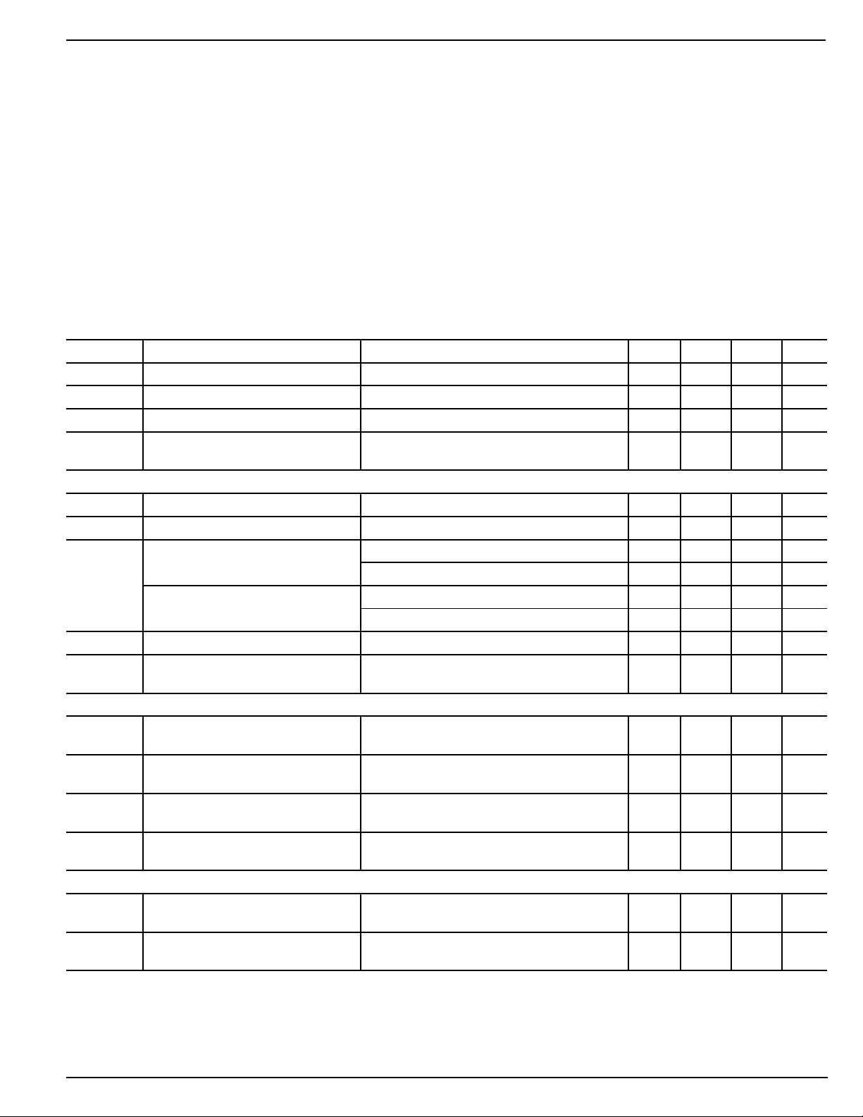
MIC4423/4424/4425 Electrical Characteristics
4.5V ≤ VS ≤ 18V; TA = 25°C, bold values indicate –40°C ≤ TA ≤ +85°C; unless noted.
Symbol Parameter Conditions Min Typ Max Units
Input
V
IH
V
IL
I
IN
Output
V
OH
V
OL
R
O
I
PK
I Latch-Up Protection >500 mA
Switching Time (Note 4)
t
R
t
F
t
D1
t
D2
Power Supply
I
S
I
S
Logic 1 Input Voltage 2.4 V
Logic 0 Input Voltage 0.8 V
Input Current 0V ≤ VIN ≤ V
S
–1 1 µA
–10 10 µA
High Output Voltage
VS–0.025
V
Low Output Voltage 0.025 V
Output Resistance HI State I
Output Resistance LO State I
= 10mA, VS = 18V 2.8 5 Ω
OUT
VIN = 0.8V, I
= 10mA, VS = 18V 3.5 5 Ω
OUT
VIN = 2.4V, I
= 10mA, VS = 18V 3.7 8 Ω
OUT
= 10mA, VS = 18V 4.3 8 Ω
OUT
Peak Output Current 3A
Withstand Reverse Current
Rise Time test Figure 1, CL = 1800pF 23 35 ns
28 60 ns
Fall Time test Figure 1, CL = 1800pF 25 35 ns
32 60 ns
Delay Tlme test Ffigure 1, CL = 1800pF 33 75 ns
32 100 ns
Delay Time test Figure 1, CL = 1800pF 38 75 ns
38 100 ns
Power Supply Current VIN = 3.0V (both inputs) 1.5 2.5 mA
2 3.5 mA
Power Supply Current VIN = 0.0V (both inputs) 0.15 0.25 mA
0.2 0.3 mA
Note 1. Exceeding the absolute maximum rating may damage the device.
Note 2. The device is not guaranteed to function outside its operating rating.
Note 3. Devices are ESD sensitive. Handling precautions recommended. ESD tested to human body model, 1.5k in series with 100pF.
Note 4. Switching times guaranteed by design.
January 1999 3 MIC4423/4424/4425
Page 4
MIC4423/4424/4425 Micrel
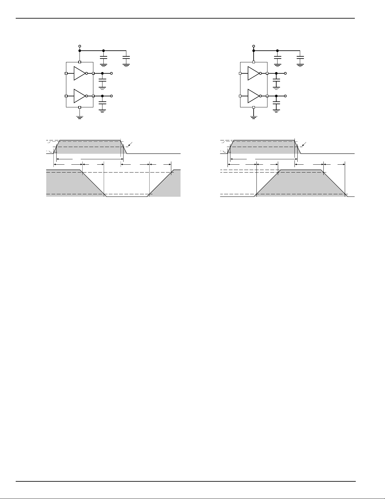
Test Circuit
INPUT
OUTPUT
VS = 18V
0.1µF 4.7µF
OUTA
1800pF
OUTB
1800pF
2.5V
t
D2
t
PW
≥ 0.5µs
5V
90%
10%
0V
V
90%
MIC4423
t
D1
A
B
t
PW
t
F
INA
INB
S
10%
0V
Figure 1a. Inverting Driver Switching Time
VS = 18V
0.1µF 4.7µF
INA
INB
A
MIC4424
B
5V
90%
INPUT
10%
0V
t
R
V
90%
S
t
PW
t
D1
t
R
OUTA
1800pF
OUTB
1800pF
2.5V
t
D2
t
PW
≥ 0.5µs
t
F
OUTPUT
10%
0V
Figure 1b. Noninverting Driver Switching Time
MIC4423/4424/4425 4 January 1999
Page 5

MIC4423/4424/4425 Micrel
0
20
40
60
80
100
4 6 8 1012141618
T
FALL
(ns)
V
SUPPLY
(V)
0
10
20
30
40
-75 -30 15 60 105 150
TIME (ns)
JUNCTION TEMPERATURE (˚C)
0
10
20
30
40
50
60
70
80
90
100
10 100 1000
I
SUPPLY
(mA)
FREQUENCY (kHz)
0
10
20
30
40
50
60
70
80
90
100
100 1000 10000
I
SUPPLY
(mA)
C
LOAD
(pF)
Typical Characteristic Curves
Rise Time vs.
100
(ns)
RISE
T
80
60
40
20
Supply Voltage
4700pF
V
SUPPLY
1800pF
1000pF
(V)
3300pF
2200pF
470pF
0
4 6 8 1012141618
Fall Time vs.
100
80
60
(ns)
FALL
40
T
20
Capacitive Load
5V
12V
18V
Fall Time vs.
Supply Voltage
4700pF
1800pF
3300pF
2200pF
470pF
Rise and Fall Time
vs. Temperature
VS = 18V
C
= 1800pF
LOAD
1000pF
T
F
T
R
Rise Time
vs. Capacitive Load
100
80
60
(ns)
RISE
40
T
20
0
100 1000 10000
C
LOAD
5V
12V
18V
(pF)
Propagation Delay vs.
50
40
30
T (ns)
20
10
Input Amplitude
VS = 18V
C
= 1800pF
LOAD
T
D2
T
D1
0
100 1000 10000
Supply Current vs.
100
V
SUPPLY
90
80
70
60
(mA)
50
40
SUPPLY
I
30
20
10
0
100 1000 10000
100
V
SUPPLY
90
80
70
60
(mA)
50
40
SUPPLY
I
30
20
10
0
10 100 1000
January 1999 5 MIC4423/4424/4425
C
(pF)
LOAD
Capacitive Load
= 18V
500kHz
20kHz
100kHz
C
(pF)
LOAD
Supply Current
vs. Frequency
= 12V
10000pF
1000pF
100pF
FREQUENCY (kHz)
3300pF
Supply Current
vs. Frequency
V
= 18V
SUPPLY
10000pF
1000pF
100pF
Supply Current vs.
Capacitive Load
V
= 5V
SUPPLY
100kHz
2MHz
3300pF
500kHz
0
024681012
INPUT (V)
Supply Current vs.
100
90
80
70
60
(mA)
50
40
SUPPLY
I
30
20
10
Capacitive Load
V
= 12V
SUPPLY
2MHz
500kHz
20kHz
100kHz
0
100 1000 10000
C
LOAD
(pF)
Supply Current
100
90
80
70
60
(mA)
50
40
SUPPLY
I
30
20
10
0
vs. Frequency
V
= 5V
SUPPLY
10000pF
4700pF
2200pF
1000pF
100pF
10 100 1000
FREQUENCY (kHz)
Page 6

MIC4423/4424/4425 Micrel
Delay Time vs.
60
50
40
30
T (ns)
20
10
Supply Voltage
C
= 2200 pF
LOAD
T
D2
T
D1
0
4 6 8 1012141618
V
SUPPLY
(V)
Quiescent Current
1.4
1.2
1.0
(mA)
0.8
0.6
QUIESCENT
0.4
I
0.2
vs. Temperature
VS = 10V
INPUTS = 1
INPUTS = 0
0
-55 -25 5 35 65 95 125
TEMPERATURE (˚C)
Delay Time
60
50
40
30
T (ns)
20
10
vs. Temperature
C
= 2200 pF
LOAD
T
D2
T
D1
0
-55 -25 5 35 65 95 125
TEMPERATURE (˚C)
Output Resistance (Output
High) vs. Supply Voltage
6
5
4
(Ω)
3
DS(ON)
R
2
1
0
4 6 8 1012141618
V
SUPPLY
125˚C
25˚C
(V)
Quiescent Supply Current
10
1
(mA)
0.1
QUIESCENT
I
0.01
4 6 8 1012141618
vs. Voltage
TJ = 25˚C
BOTH INPUTS = 1
BOTH INPUTS = 0
V
SUPPLY
(V)
Output Resistance (Output
Low) vs. Supply Voltage
6
5
4
(Ω)
3
DS(ON)
R
2
1
0
4 6 8 1012141618
V
SUPPLY
125˚C
25˚C
(V)
MIC4423/4424/4425 6 January 1999
Page 7

MIC4423/4424/4425 Micrel
Application Information
Although the MIC4423/24/25 drivers have been specifically
constructed to operate reliably under any practical
circumstances, there are nonetheless details of usage which
will provide better operation of the device.
Supply Bypassing
Charging and discharging large capacitive loads quickly
requires large currents. For example, charging 2000pF from
0 to 15 volts in 20ns requires a constant current of 1.5A. In
practice, the charging current is not constant, and will usually
peak at around 3A. In order to charge the capacitor, the driver
must be capable of drawing this much current, this quickly,
from the system power supply. In turn, this means that as far
as the driver is concerned, the system power supply, as seen
by the driver, must have a VERY low impedance.
As a practical matter, this means that the power supply bus
must be capacitively bypassed at the driver with at least 100X
the load capacitance in order to achieve optimum driving
speed. It also implies that the bypassing capacitor must have
very low internal inductance and resistance at all frequencies
of interest. Generally, this means using two capacitors, one a
high-performance low ESR film, the other a low internal
resistance ceramic, as together the valleys in their two
impedance curves allow adequate performance over a broad
enough band to get the job done. PLEASE NOTE that many
film capacitors can be sufficiently inductive as to be useless
for this service. Likewise, many multilayer ceramic capacitors
have unacceptably high internal resistance. Use capacitors
intended for high pulse current service (in-house we use
WIMA™ film capacitors and AVX Ramguard™ ceramics;
several other manufacturers of equivalent devices also exist).
The high pulse current demands of capacitive drivers also
mean that the bypass capacitors must be mounted very close
to the driver in order to prevent the effects of lead inductance
or PCB land inductance from nullifying what you are trying to
accomplish. For optimum results the sum of the lengths of the
leads and the lands from the capacitor body to the driver body
should total 2.5cm or less.
Bypass capacitance, and its close mounting to the driver
serves two purposes. Not only does it allow optimum
performance from the driver, it minimizes the amount of lead
length radiating at high frequency during switching, (due to the
large ∆ I) thus minimizing the amount of EMI later available for
system disruption and subsequent cleanup. It should also be
noted that the actual frequency of the EMI produced by a
driver is not the clock frequency at which it is driven, but is
related to the highest rate of change of current produced
during switching, a frequency generally one or two orders of
magnitude higher, and thus more difficult to filter if you let it
permeate your system.
to proper operation of high speed driver ICs.
Grounding
Both proper bypassing and proper grounding are necessary
for optimum driver operation. Bypassing capacitance only
allows a driver to turn the load ON. Eventually (except in rare
circumstances) it is also necessary to turn the load OFF. This
Good bypassing practice is essential
requires attention to the ground path. Two things other than
the driver affect the rate at which it is possible to turn a load
off: The adequacy of the grounding available for the driver,
and the inductance of the leads from the driver to the load. The
latter will be discussed in a separate section.
Best practice for a ground path is obviously a well laid out
ground plane. However, this is not always practical, and a
poorly-laid out ground plane can be worse than none. Attention
to the paths taken by return currents even in a ground plane
is essential. In general, the leads from the driver to its load, the
driver to the power supply, and the driver to whatever is driving
it should all be as low in resistance and inductance as
possible. Of the three paths, the ground lead from the driver
to the logic driving it is most sensitive to resistance or
inductance, and ground current from the load are what is most
likely to cause disruption. Thus, these ground paths should be
arranged so that they never share a land, or do so for as short
a distance as is practical.
To illustrate what can happen, consider the following: The
inductance of a 2cm long land, 1.59mm (0.062") wide on a
PCB with no ground plane is approximately 45nH. Assuming
a dl/dt of 0.3A/ns (which will allow a current of 3A to flow after
10ns, and is thus slightly slow for our purposes) a voltage of
13.5 Volts will develop along this land in response to our
postulated ∆Ι. For a 1cm land, (approximately 15nH) 4.5 Volts
is developed. Either way, anyone using TTL-level input signals
to the driver will find that the response of their driver has been
seriously degraded by a common ground path for input to and
output from the driver of the given dimensions. Note that this
is before accounting for any resistive drops in the circuit. The
resistive drop in a 1.59mm (0.062") land of 2oz. Copper
carrying 3A will be about 4mV/cm (10mV/in) at DC, and the
resistance will increase with frequency as skin effect comes
into play.
The problem is most obvious in inverting drivers where the
input and output currents are in phase so that any attempt to
raise the driver’s input voltage (in order to turn the driver’s load
off) is countered by the voltage developed on the common
ground path as the driver attempts to do what it was supposed
to. It takes very little common ground path, under these
circumstances, to alter circuit operation drastically.
Output Lead Inductance
The same descriptions just given for PCB land inductance
apply equally well for the output leads from a driver to its load,
except that commonly the load is located much further away
from the driver than the driver’s ground bus.
Generally, the best way to treat the output lead inductance
problem, when distances greater than 4cm (2") are involved,
requires treating the output leads as a transmission line.
Unfortunately, as both the output impedance of the driver and
the input impedance of the MOSFET gate are at least an order
of magnitude lower than the impedance of common coax,
using coax is seldom a cost-effective solution. A twisted pair
works about as well, is generally lower in cost, and allows use
of a wider variety of connectors. The second wire of the
twisted pair should carry common from as close as possible
January 1999 7 MIC4423/4424/4425
Page 8

MIC4423/4424/4425 Micrel
to the ground pin of the driver directly to the ground terminal
of the load. Do not use a twisted pair where the second wire
in the pair is the output of the other driver, as this will not
provide a complete current path for either driver. Likewise, do
not use a twisted triad with two outputs and a common return
unless both of the loads to be driver are mounted extremely
close to each other, and you can guarantee that they will never
be switching at the same time.
For output leads on a printed circuit, the general rule is to
make them as short and as wide as possible. The lands should
also be treated as transmission lines: i.e. minimize sharp
bends, or narrowings in the land, as these will cause ringing.
For a rough estimate, on a 1.59mm (0.062") thick G-10 PCB
a pair of opposing lands each 2.36mm (0.093") wide translates
to a characteristic impedance of about 50Ω. Half that width
suffices on a 0.787mm (0.031") thick board. For accurate
impedance matching with a MIC4423/24/25 driver, on a
1.59mm (0.062") board a land width of 42.75mm (1.683")
would be required, due to the low impedance of the driver and
(usually) its load. This is obviously impractical under most
circumstances. Generally the tradeoff point between lands
and wires comes when lands narrower than 3.18mm (0.125")
would be required on a 1.59mm (0.062") board.
To obtain minimum delay between the driver and the load, it
is considered best to locate the driver as close as possible to
the load (using adequate bypassing). Using matching
transformers at both ends of a piece of coax, or several
matched lengths of coax between the driver and the load,
works in theory, but is not optimum.
Driving at Controlled Rates
Occasionally there are situations where a controlled rise or fall
time (which may be considerably longer than the normal rise
or fall time of the driver’s output) is desired for a load. In such
cases it is still prudent to employ best possible practice in
terms of bypassing, grounding and PCB layout, and then
reduce the switching speed of the load (NOT the driver) by
adding a noninductive series resistor of appropriate value
between the output of the driver and the load. For situations
where only rise or only fall should be slowed, the resistor can
be paralleled with a fast diode so that switching in the other
direction remains fast. Due to the Schmitt-trigger action of the
driver’s input it is not possible to slow the rate of rise (or fall)
of the driver’s input signal to achieve slowing of the output.
Input Stage
The input stage of the MIC4423/24/25 consists of a singleMOSFET class A stage with an input capacitance of ≤38pF.
This capacitance represents the maximum load from the
driver that will be seen by its controlling logic. The drain load
on the input MOSFET is a –2mA current source. Thus, the
quiescent current drawn by the driver varies, depending on
the logic state of the input.
Following the input stage is a buffer stage which provides
~400mV of hysteresis for the input, to prevent oscillations
when slowly-changing input signals are used or when noise is
present on the input. Input voltage switching threshold is
approximately 1.5V which makes the driver directly compatible
with TTL signals, or with CMOS powered from any supply
voltage between 3V and 15V.
The MIC4423/24/25 drivers can also be driven directly by the
SG1524/25/26/27, TL494/95, TL594/95, NE5560/61/62/68,
TSC170, MIC38C42, and similar switch mode power supply
ICs. By relocating the main switch drive function into the driver
rather than using the somewhat limited drive capabilities of a
PWM IC. The PWM IC runs cooler, which generally improves
its performance and longevity, and the main switches switch
faster, which reduces switching losses and increase system
efficiency.
The input protection circuitry of the MIC4423/24/25, in addition
to providing 2kV or more of ESD protection, also works to
prevent latchup or logic upset due to ringing or voltage spiking
on the logic input terminal. In most CMOS devices when the
logic input rises above the power supply terminal, or descends
below the ground terminal, the device can be destroyed or
rendered inoperable until the power supply is cycled OFF and
ON. The MIC4423/24/25 drivers have been designed to
prevent this. Input voltages excursions as great as 5V below
ground will not alter the operation of the device. Input excursions
above the power supply voltage will result in the excess
voltage being conducted to the power supply terminal of the
IC. Because the excess voltage is simply conducted to the
power terminal, if the input to the driver is left in a high state
when the power supply to the driver is turned off, currents as
high as 30mA can be conducted through the driver from the
input terminal to its power supply terminal. This may overload
the output of whatever is driving the driver, and may cause
other devices that share the driver’s power supply, as well as
the driver, to operate when they are assumed to be off, but it
will not harm the driver itself. Excessive input voltage will also
slow the driver down, and result in much longer internal
propagation delays within the drivers. TD2, for example, may
increase to several hundred nanoseconds. In general, while
the driver will accept this sort of misuse without damage,
proper termination of the line feeding the driver so that line
spiking and ringing are minimized, will always result in faster
and more reliable operation of the device, leave less EMI to be
filtered elsewhere, be less stressful to other components in
the circuit, and leave less chance of unintended modes of
operation.
Power Dissipation
CMOS circuits usually permit the user to ignore power
dissipation. Logic families such as 4000 series and 74Cxxx
have outputs which can only source or sink a few milliamps of
current, and even shorting the output of the device to ground
or VCC may not damage the device. CMOS drivers, on the
other hand, are intended to source or sink several Amps of
current. This is necessary in order to drive large capacitive
loads at frequencies into the megahertz range. Package
power dissipation of driver ICs can easily be exceeded when
driving large loads at high frequencies. Care must therefore
be paid to device dissipation when operating in this domain.
The Supply Current vs Frequency and Supply Current vs
Load characteristic curves furnished with this data sheet aid
MIC4423/4424/4425 8 January 1999
Page 9

MIC4423/4424/4425 Micrel
in estimating power dissipation in the driver. Operating
frequency, power supply voltage, and load all affect power
dissipation.
Given the power dissipation in the device, and the thermal
resistance of the package, junction operating temperature for
any ambient is easy to calculate. For example, the thermal
resistance of the 8-pin plastic DIP package, from the datasheet,
is 150°C/W. In a 25°C ambient, then, using a maximum
junction temperature of 150°C, this package will dissipate
960mW.
Accurate power dissipation numbers can be obtained by
summing the three sources of power dissipation in the device:
• Load power dissipation (PL)
• Quiescent power dissipation (PQ)
• Transition power dissipation (PT)
Calculation of load power dissipation differs depending on
whether the load is capacitive, resistive or inductive.
Resistive Load Power Dissipation
Dissipation caused by a resistive load can be calculated as:
PL = I2 RO D
where:
I = the current drawn by the load
RO = the output resistance of the driver when the
output is high, at the power supply voltage used
(See characteristic curves)
D = fraction of time the load is conducting (duty cycle)
Capacitive Load Power Dissipation
Dissipation caused by a capacitive load is simply the energy
placed in, or removed from, the load capacitance by the driver.
The energy stored in a capacitor is described by the equation:
E = 1/2 C V
2
As this energy is lost in the driver each time the load is charged
or discharged, for power dissipation calculations the 1/2 is
removed. This equation also shows that it is good practice not
to place more voltage in the capacitor than is necessary, as
dissipation increases as the square of the voltage applied to
the capacitor. For a driver with a capacitive load:
PL = f C (VS)
2
where:
f = Operating Frequency
C = Load Capacitance
VS = Driver Supply Voltage
Inductive Load Power Dissipation
For inductive loads the situation is more complicated. For the
part of the cycle in which the driver is actively forcing current
into the inductor, the situation is the same as it is in the
resistive case:
PL1 = I2 RO D
However, in this instance the RO required may be either the
on resistance of the driver when its output is in the high state,
or its on resistance when the driver is in the low state,
depending on how the inductor is connected, and this is still
only half the story. For the part of the cycle when the inductor
is forcing current through the driver, dissipation is best
described as
PL2 = I VD (1 – D)
where VD is the forward drop of the clamp diode in the driver
(generally around 0.7V). The two parts of the load dissipation
must be summed in to produce P
PL = PL1 + P
L2
L
Quiescent Power Dissipation
Quiescent power dissipation (PQ, as described in the input
section) depends on whether the input is high or low. A low
input will result in a maximum current drain (per driver) of
≤0.2mA; a logic high will result in a current drain of ≤2.0mA.
Quiescent power can therefore be found from:
PQ = VS [D IH + (1 – D) IL]
where:
IH = quiescent current with input high
IL = quiescent current with input low
D = fraction of time input is high (duty cycle)
VS = power supply voltage
Transition Power Dissipation
Transition power is dissipated in the driver each time its output
changes state, because during the transition, for a very brief
interval, both the N- and P-channel MOSFETs in the output
totem-pole are ON simultaneously, and a current is conducted
through them from VS to ground. The transition power
dissipation is approximately:
PT = f VS (A•s)
where (A•s) is a time-current factor derived from Figure 2.
Total power (PD) then, as previously described is just
PD = PL + PQ +P
T
Examples show the relative magnitude for each term.
EXAMPLE 1: A MIC4423 operating on a 12V supply driving
two capacitive loads of 3000pF each, operating at 250kHz,
with a duty cycle of 50%, in a maximum ambient of 60°C.
First calculate load power loss:
PL = f x C x (VS)
PL= 250,000 x (3 x 10–9 + 3 x 10–9) x 12
2
2
= 0.2160W
Then transition power loss:
PT = f x VS x (A•s)
= 250,000 • 12 • 2.2 x 10–9 = 6.6mW
Then quiescent power loss:
PQ= VS x [D x IH + (1 – D) x IL]
January 1999 9 MIC4423/4424/4425
Page 10

MIC4423/4424/4425 Micrel
= 12 x [(0.5 x 0.0035) + (0.5 x 0.0003)]
= 0.0228W
Total power dissipation, then, is:
PD= 0.2160 + 0.0066 + 0.0228
= 0.2454W
Assuming an SOIC package, with an θJA of 120°C/W, this will
result in the junction running at:
0.2454 x 120 = 29.4°C
above ambient, which, given a maximum ambient temperature
of 60°C, will result in a maximum junction temperature of
89.4°C.
EXAMPLE 2: A MIC4424 operating on a 15V input, with one
driver driving a 50Ω resistive load at 1MHz, with a duty cycle
of 67%, and the other driver quiescent, in a maximum ambient
temperature of 40°C:
PL = I2 x RO x D
First, IO must be determined.
IO = VS / (RO + R
LOAD
)
Given RO from the characteristic curves then,
IO = 15 / (3.3 + 50)
IO = 0.281A
and:
PL= (0.281)2 x 3.3 x 0.67
= 0.174W
PT= F x VS x (A•s)/2
(because only one side is operating)
= (1,000,000 x 15 x 3.3 x 10–9) / 2
= 0.025 W
and:
= 0.213W
In a ceramic package with an θJA of 100°C/W, this amount of
power results in a junction temperature given the maximum
40°C ambient of:
(0.213 x 100) + 40 = 61.4°C
The actual junction temperature will be lower than calculated
both because duty cycle is less than 100% and because the
graph lists R
at a TJ of 125°C and the R
DS(on)
DS(on)
at 61°C
TJ will be somewhat lower.
Definitions
CL = Load Capacitance in Farads.
D = Duty Cycle expressed as the fraction of time the input
to the driver is high.
f = Operating Frequency of the driver in Hertz
IH = Power supply current drawn by a driver when both
inputs are high and neither output is loaded.
IL = Power supply current drawn by a driver when both
inputs are low and neither output is loaded.
ID = Output current from a driver in Amps.
PD = Total power dissipated in a driver in Watts.
PL = Power dissipated in the driver due to the driver’s load
in Watts.
PQ = Power dissipated in a quiescent driver in Watts.
PT = Power dissipated in a driver when the output changes
states (“shoot-through current”) in Watts. NOTE: The
“shoot-through” current from a dual transition (once
up, once down) for both drivers is stated in the graph
on the following page in ampere-nanoseconds. This
figure must be multiplied by the number of repetitions
per second (frequency to find Watts).
PQ = 15 x [(0.67 x 0.00125) + (0.33 x 0.000125) +
(1 x 0.000125)]
RO= Output resistance of a driver in Ohms.
VS= Power supply voltage to the IC in Volts.
(this assumes that the unused side of the driver has its input
grounded, which is more efficient)
= 0.015W
then:
PD= 0.174 + 0.025 + 0.0150
MIC4423/4424/4425 10 January 1999
Page 11

MIC4423/4424/4425 Micrel
Crossover
-8
10
-9
10
A•s (Ampere-seconds)
-10
10
0 2 4 6 8 1012141618
Energy Loss
V
IN
NOTE: THE VALUES ON THIS GRAPH REPRESENT THE LOSS SEEN BY BOTH
DRIVERS IN A PACKAGE DURING ONE COMPLETE CYCLE. FOR A SINGLE
DRIVER DIVIDE THE STATED VALUES BY 2. FOR A SINGLE TRANSITION OF A
SINGLE DRIVER, DIVIDE THE STATED VALUE BY 4.
Figure 2.
1250
1000
SOIC
750
500
MAXIMUM PACKAGE
250
POWER DISSIPATION (mW)
0
25 50 15075 100
PDIP
125
AMBIENT TEMPERATURE (°C)
January 1999 11 MIC4423/4424/4425
Page 12

MIC4423/4424/4425 Micrel
Package Information
PIN 1
DIMENSIONS:
INCH (MM)
0.018 (0.57)
0.100 (2.54)
0.026 (0.65)
MAX)
0.157 (3.99)
0.150 (3.81)
0.050 (1.27)
0.064 (1.63)
0.045 (1.14)
0.380 (9.65)
0.370 (9.40)
TYP
0.197 (5.0)
0.189 (4.8)
0.135 (3.43)
0.125 (3.18)
0.130 (3.30)
0.0375 (0.952)
8-Pin DIP (N)
PIN 1
0.020 (0.51)
0.013 (0.33)
0.0098 (0.249)
0.0040 (0.102)
0°–8°
SEATING
PLANE
0.380 (9.65)
0.320 (8.13)
DIMENSIONS:
INCHES (MM)
0.050 (1.27)
0.016 (0.40)
0.244 (6.20)
0.228 (5.79)
0.255 (6.48)
0.245 (6.22)
0.300 (7.62)
0.013 (0.330)
0.010 (0.254)
45°
0.010 (0.25)
0.007 (0.18)
8-Pin SOIC (M)
PIN 1
DIMENSIONS:
MIN
INCHES (MM)
7°
TYP
R
0.297 (7.544)
0.293 (7.442)
0.330 (8.382)
0.326 (8.280)
0.032 (0.813) TYP
0.408 (10.363)
0.404 (10.262)
0.022 (0.559)
0.018 (0.457)
10° TYP
5°
TYP
0.301 (7.645)
0.297 (7.544)
0.027 (0.686)
0.031 (0.787)
0.094 (2.388)
0.090 (2.286)
0.050 (1.270)
TYP
0.409 (10.389)
0.405 (10.287)
0.016 (0.046)
TYP
0.103 (2.616)
0.099 (2.515)
SEATING
PLANE
0.015
(0.381)
0.015
(0.381)
16-Pin Wide SOIC (WM)
MICREL INC. 1849 FORTUNE DRIVE SAN JOSE, CA 95131 USA
TEL + 1 (408) 944-0800 FAX + 1 (408) 944-0970 WEB http://www.micrel.com
This information is believed to be accurate and reliable, however no responsibility is assumed by Micrel for its use nor for any infringement of patents or
other rights of third parties resulting from its use. No license is granted by implication or otherwise under any patent or patent right of Micrel Inc.
© 1999 Micrel Incorporated
MIC4423/4424/4425 12 January 1999
 Loading...