

Datasheet MCM32A932SG33, MCM32A964SG33, MCM32A764SG33, MCM32A832SG33, MCM32A732SG33 Datasheet (Motorola)
...Page 1
MCM32A732/764•MCM32A832/864•MCM32A932/964
1
MOTOROLA FAST SRAM
Advance Information
128KB/256KB Secondary Cache
Module
With Tag, Valid, and Dirty for i486
Processor Systems
This family of cache modules is well suited to provide the secondary cache for
the Intel 82420 PCI chipset. This family provides the 128K Byte and 256K Byte
cache sizes with valid, dirty and a choice of 7, 8, or 9 tag bits. The tag/valid bits
have 12 ns access times for zero wait states at 33 MHz clock speeds. The PD
pins map into the configuration register of the 82420 for auto–configuration of the
cache controller during system startup.
• Low Profile Edge Connector: Burndy Part Number: CELP2X56SC3Z48
• Single 5 V ± 10% Power Supply
• All Inputs and Outputs are TTL Compatible
• Three State Outputs
• Fast Module Cycle Time: Up to External Processor Bus Speed of 33 MHz
• Cache Byte Write, Bank Chip Enable, Bank Output Enable
• Decoupling Capacitors are Used for Each Fast Static RAM
• High Quality Multi–Layer FR4 PWB With Separate Power and Ground Planes
BurstRAM is a registered trademark of Motorola.
I486 is a registered trademark Intel Corp.
This document contains information on a new product. Specifications and information herein are subject to change without notice.
Order this document
by MCM32A732/D
MOTOROLA
SEMICONDUCTOR TECHNICAL DATA
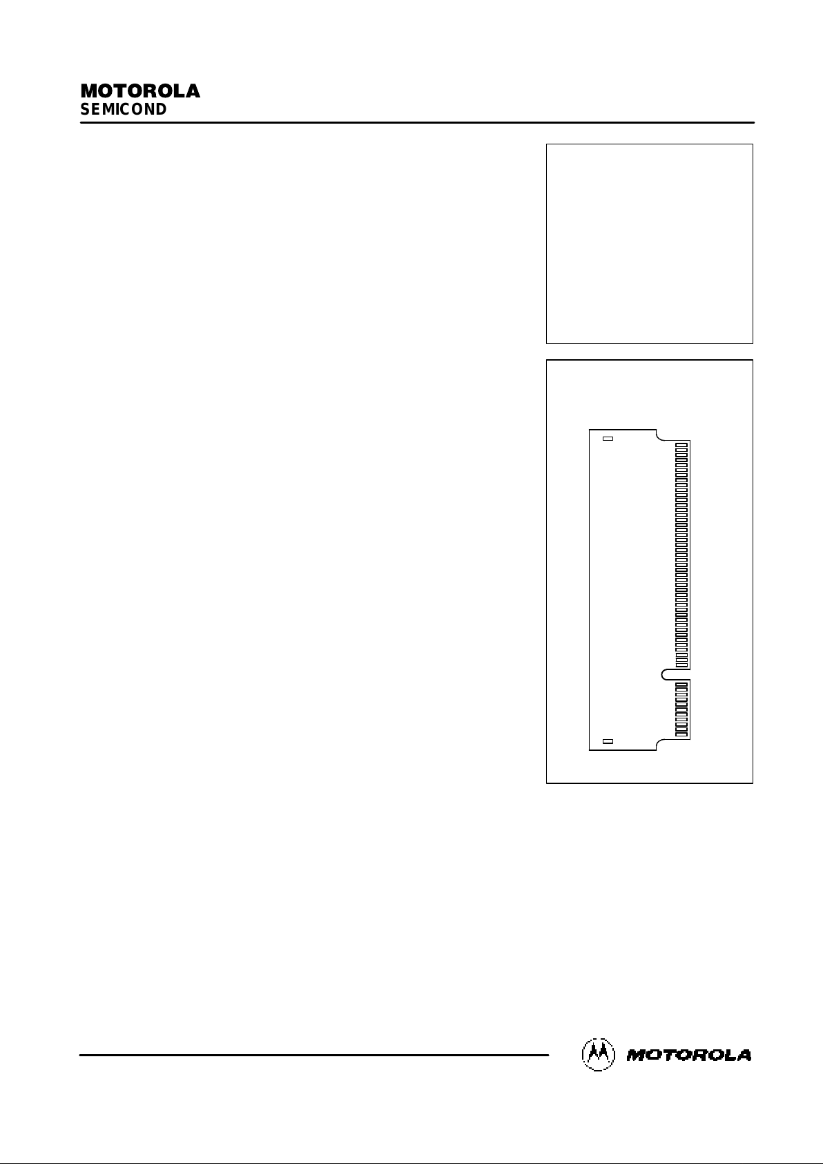
MCM32A732
MCM32A832
MCM32A932
MCM32A764
MCM32A864
MCM32A964
56
46
45
1
112–LEAD
CARD EDGE
CASE 1112–01
TOP VIEW
REV 1
6/95
Motorola, Inc. 1994
Page 2
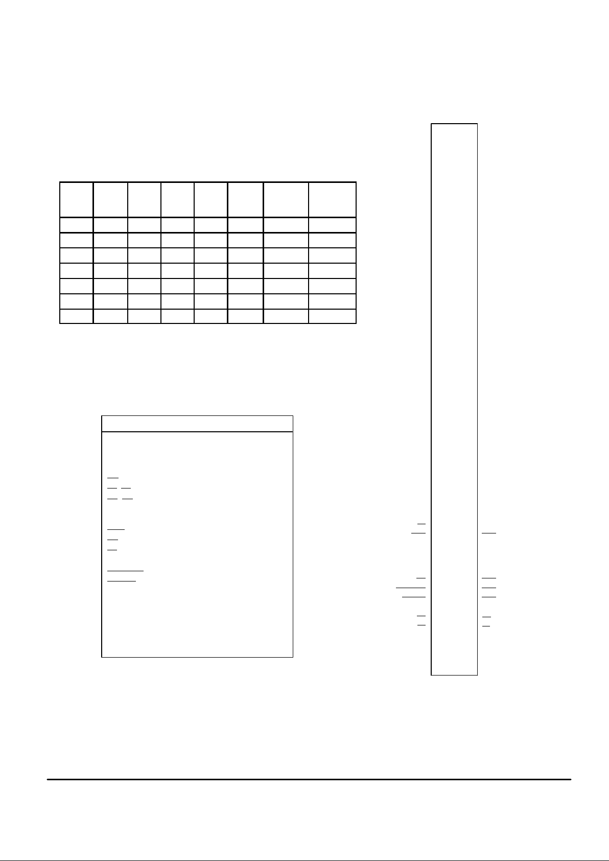
PIN ASSIGNMENT
CACHE MODULE
112–LEAD CARDEDGE
TOP VIEW
V
SS
DQ0
DQ2
DQ4
DQ6
V
CC
NC
DQ8
DQ10
DQ12
V
SS
DQ14
DQ16
DQ18
DQ20
V
CC
DQ22
NC
DQ24
DQ26
V
SS
DQ28
DQ30
LA2
LA3
V
CC
A4
A6
A8
A10
A12
A14
A16
NC
V
SS
DIRTYD
TDQ0
TDQ2
TDQ4
V
SS
TDQ6
VALID
TE
TWE
V
CC
1
2
3
4
5
6
7
8
9
10
11
12
13
14
15
16
17
18
19
20
21
22
23
24
25
26
27
28
29
30
31
32
33
34
35
36
37
38
39
40
41
42
43
44
45
V
SS
DQ1
DQ3
DQ5
DQ7
V
CC
NC
DQ9
DQ11
DQ13
V
SS
DQ15
DQ17
DQ19
DQ21
V
CC
DQ23
NC
DQ25
DQ27
V
SS
DQ29
DQ31
HA2
HA3
V
CC
A5
A7
A9
A11
A13
A15
NC
NC
V
SS
DIRTYQ
TDQ1
TDQ3
TDQ5
V
SS
TDQ7*
TDQ8**
ALE
WE0
V
CC
57
58
59
60
61
62
63
64
65
66
67
68
69
70
71
72
73
74
75
76
77
78
79
80
81
82
83
84
85
86
87
88
89
90
91
92
93
94
95
96
97
98
99
100
101
V
SS
G1
E1
PD1
PD3
NC
V
SS
46
47
48
49
50
51
52
53
54
55
56
102
103
104
105
106
107
108
109
110
111
112
V
SS
TG
DIRTYWE
DIRTYE
V
CC
G0
E0
PD0
PD2
PD4
V
SS
WE1
WE2
WE3
V
CC
PIN NAMES
A4 – A19 Address Inputs. . . . . . . . . . . . . . . . . . . . . .
HCA2, HCA3 Upper Bank Address Inputs. . . . . . .
LCA2, LCA3 Lower Bank Address Inputs. . . . . . . .
ALE Address Latch Enable. . . . . . . . . . . . . . . . . . . .
Wx
Byte Write Enable. . . . . . . . . . . . . . . . . . . . . . . .
E0
, E1 Bank Chip Enable. . . . . . . . . . . . . . . . . . . . .
G0
, G1 Bank Output Enable. . . . . . . . . . . . . . . . . . .
DQ0 – DQ31 Cache Data Input/Output. . . . . . . . . .
TDQ0 – TDQ8 Tag Data Input/Output. . . . . . . . . . .
TWE
Tag Write Enable. . . . . . . . . . . . . . . . . . . . . . . .
TG
Tag Output Enable. . . . . . . . . . . . . . . . . . . . . . . .
TE
Tag Chip Enable. . . . . . . . . . . . . . . . . . . . . . . . . .
VALID Valid Bit. . . . . . . . . . . . . . . . . . . . . . . . . . . . . .
DIRTYWE Dirty Write Enable. . . . . . . . . . . . . . . . . .
DIRTYE
Dirty Chip Enable. . . . . . . . . . . . . . . . . . . . .
DIRTYD Dirty Data Input. . . . . . . . . . . . . . . . . . . . . .
DIRTYQ Dirty Data Output. . . . . . . . . . . . . . . . . . . . .
PD0 – PD4 Presence Detect. . . . . . . . . . . . . . . . . .
NC No Connect. . . . . . . . . . . . . . . . . . . . . . . . . . . . . .
V
CC
+5 V Power Supply. . . . . . . . . . . . . . . . . . . . . .
V
SS
Ground. . . . . . . . . . . . . . . . . . . . . . . . . . . . . . . .
* No Connect for 32A864, 32A832
** No Connect for 32A764, 32A864, 32A732, 32A832
MCM32A732/764•MCM32A832/864•MCM32A932/964
2
MOTOROLA FAST SRAM
PD4 PD3 PD2 PD1 PD0
Cache
Size
Main
Memory
Max
Module
NC NC NC NC NC — — No Module
V
CC
V
CC
NC NC V
CC
128KB 16MB 32A732
V
CC
NC NC NC V
CC
128KB 32MB 32A832
V
CC
NC V
CC
NC V
CC
128KB 64MB 32A932
V
CC
V
CC
NC V
CC
NC 256KB 32MB 32A764
V
CC
NC NC V
CC
NC 256KB 64MB 32A864
V
CC
NC V
CC
V
CC
NC 256KB 128MB 32A964
Page 3
MCM32A732/764•MCM32A832/864•MCM32A932/964
3
MOTOROLA FAST SRAM
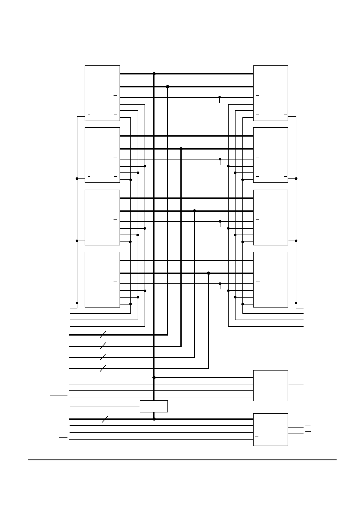
486 256KB CACHE MODULE BLOCK DIAGRAM
WITH 9 TAG BITS
A2 – A14 A2 – A14
DQ0 – DQ7 DQ0 – DQ7
W
A1
G
A0
E
32K x 8
W
A1
G
A0
E
32K x 8
W0
A2 – A14 A2 – A14
DQ0 – DQ7 DQ0 – DQ7
W
A1
G
A0
E
32K x 8
W
A1
G
A0
E
32K x 8
W1
A2 – A14 A2 – A14
DQ0 – DQ7 DQ0 – DQ7
W
A1
G
A0
E
32K x 8
W
A1
G
A0
E
32K x 8
W2
A2 – A14 A2 – A14
DQ0 – DQ7 DQ0 – DQ7
W
A1
G
A0
E
32K x 8
W
A1
G
A0
E
32K x 8
W3
E1
HCA3
G1
HCA2
E0
LCA3
G0
LCA2
DQ0 – DQ7
DQ8 – DQ15
DQ16 – DQ23
DQ24 – DQ31
DIRTYQ
DIRTYD
DIRTYWE
A0 – A13
D
in
D
out
W
16K x 1
74F373
ALE
DIRTYE
A0 – A13
DQ9
DQ0 – DQ8
W
16K x 10
TE
TG
TWE
TDQ0 – TDQ8
VALID
A4 – A17
8
8
8
8
14
Page 4
MCM32A732/764•MCM32A832/864•MCM32A932/964
4
MOTOROLA FAST SRAM
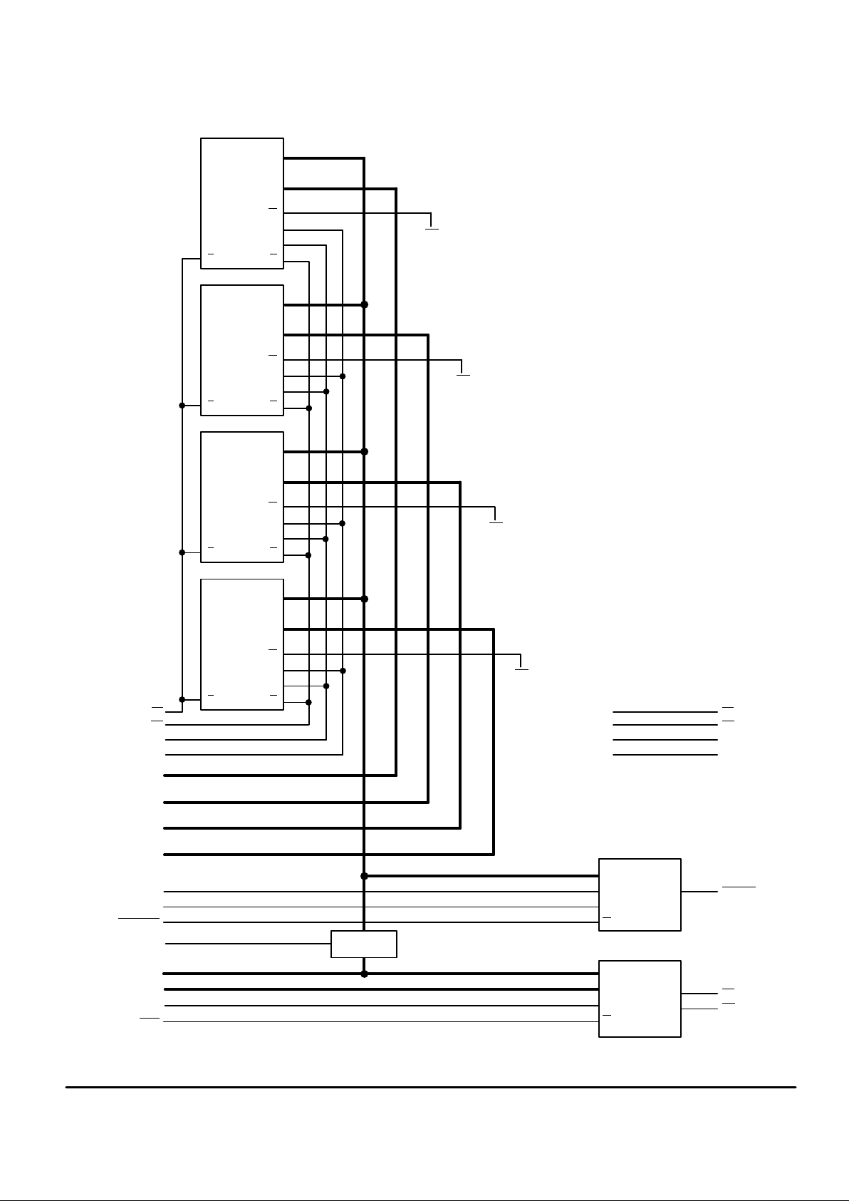
486 128KB CACHE MODULE BLOCK DIAGRAM
WITH 9 TAG BITS
A2 – A14
DQ0 – DQ7
W
A1
G
A0
E
32K x 8
W0
A2 – A14
DQ0 – DQ7
W
A1
G
A0
E
32K x 8
W1
A2 – A14
DQ0 – DQ7
W
A1
G
A0
E
32K x 8
W2
A2 – A14
DQ0 – DQ7
W
A1
G
A0
E
32K x 8
W3
E1
HCA3
G1
HCA2
E0
LCA3
G0
LCA2
DQ0 – DQ7
DQ8 – DQ15
DQ16 – DQ23
DQ24 – DQ31
DIRTYQ
DIRTYD
DIRTYWE
A0 – A12
D
in
D
out
W
8K x 1
74F373
ALE
DIRTYE
A0 – A12
DQ9
DQ0 – DQ8
W
8K x 10
TE
TG
TWE
TDQ0 – TDQ8
VALID
A4 – A17
NC
NC
NC
NC
Page 5

MCM32A732/764•MCM32A832/864•MCM32A932/964
5
MOTOROLA FAST SRAM
TRUTH TABLE (X = Don’t Care)
E
G W Mode VCC Current Output Cycle
H X X Not Selected I
SB1
, I
SB2
High–Z –
L H H Output Disabled I
CCA
High–Z –
L L H Read I
CCA
D
out
Read Cycle
L X L Write I
CCA
High–Z Write Cycle
NOTE: E = Exx, ET; W = Wxx, WT, WA; G = GA, GB
ABSOLUTE MAXIMUM RATINGS
Rating Symbol Value Unit
Power Supply Voltage V
CC
– 0.5 to + 7.0 V
Voltage Relative to VSS For Any Pin
Except V
CC
Vin, V
out
– 0.5 to VCC + 0.5 V
Output Current I
out
± 20 mA
Power Dissipation P
D
11.0 W
Temperature Under Bias T
bias
– 10 to + 85 °C
Operating Temperature T
A
0 to + 70 °C
Storage Temperature — Plastic T
stg
– 55 to + 125 °C
NOTE: Permanent device damage may occur if ABSOLUTE MAXIMUM RATINGS are
exceeded. Functional operation should be restricted to RECOMMENDED OPERATING CONDITIONS. Exposure to higher than recommended voltages for extended periods of time could affect device reliability.
DC OPERATING CONDITIONS AND CHARACTERISTICS
(VCC = 5.0 V ±10%, TA = 0 to 70°C, Unless Otherwise Noted)
RECOMMENDED OPERATING CONDITIONS
Parameter Symbol Min Typ Max Unit
Supply Voltage (Operating Voltage Range) V
CC
4.5 5.0 5.5 V
Input High Voltage V
IH
2.2 —
VCC + 0.3**
V
Input Low Voltage V
IL
– 0.5*
— 0.8 V
*VIL (min) = – 0.5 V dc; VIL (min) = – 2.0 V ac (pulse width ≤ 20 ns)
**VIH (max) = VCC + 0.3 V dc; VIH (max) = VCC + 2.0 V ac (pulse width ≤ 20 ns)
DC CHARACTERISTICS
Parameter Symbol Min Max Unit
Input Leakage Current (All Inputs, Vin = 0 to VCC) I
lkg(I)
— ±10 µA
Output Leakage Current (E = VIH or G = VIH, V
out
= 0 to VCC) I
lkg(O)
— ±10 µA
Output High Voltage (IOH = – 4.0 mA) V
OH
2.4 — V
Output Low Voltage (IOL = 8.0 mA) V
OL
— 0.4 V
POWER SUPPLY CURRENTS
Parameter Symbol
32Ax32
33 MHz
32Ax64
33 MHz
Unit
AC Active Supply Current (I
out = 0 mA, VCC
= Max, f = f
max
) I
CCA
750 1250 mA
AC Standby Current (E = VIH, VCC = Max, f = f
max)
I
SB1
180 300 mA
CMOS Standby Current (VCC = Max, f = 0 MHz, E ≥ VCC – 0.2 V
Vin ≤ VSS + 0.2 V, or ≥ VCC – 0.2 V)
I
SB2
120 200 mA
This device contains circuitry to protect the
inputs against damage due to high static voltages or electric fields; however, it is advised
that normal precautions be taken to avoid
application of any voltage higher than maximum rated voltages to this high–impedance
circuit.
This CMOS memory circuit has been designed to meet the dc and ac specifications
shown in the tables, after thermal equilibrium
has been established. The circuit is in a test
socket or mounted on a printed circuit board
and transverse air flow of at least 500 linear
feet per minute is maintained.
Page 6

MCM32A732/764•MCM32A832/864•MCM32A932/964
6
MOTOROLA FAST SRAM
CAPACITANCE (f = 1 MHz, dV = 3 V, T
A
= 25°C, Periodically sampled rather than 100% tested)
Characteristic
Symbol Max Unit
Cache Address Input Capacitance C
in
48 pF
Control Pin Input Capacitance (E, W) C
in
8 pF
I/O Capacitance C
I/O
8 pF
Tag Address Input Capacitance C
in
18 pF
AC OPERATING CONDITIONS AND CHARACTERISTICS
(VCC = 5.0 V ± 10%, TA = 0 to + 70°C, Unless Otherwise Noted)
Input Timing Measurement Reference Level 1.5 V. . . . . . . . . . . . . . .
Input Pulse Levels 0 to 3.0 V. . . . . . . . . . . . . . . . . . . . . . . . . . . . . . . . .
Input Rise/Fall Time 5 ns. . . . . . . . . . . . . . . . . . . . . . . . . . . . . . . . . . . .
Output Timing Measurement Reference Level 1.5 V. . . . . . . . . . . . .
Output Load Figure 1A Unless Otherwise Noted. . . . . . . . . . . . . . . .
READ CYCLE (See Notes 1 and 2)
Data Tag/Valid Dirty
Parameter Symbol Min Max Min Max Min Max Unit Notes
Read Cycle Time t
AVAV
30 — 30 — 30 — ns 3
Address Access Time xCA2–3
(Transparent Mode) A4 – A19
t
AVQV
t
AVQV
——2025——1212———25ns 9
Chip Select Access Time t
ELQV
— 20 — 12 — 20 ns 4
Output Enable to Output Valid t
GLQV
— 10 — 6 — — ns
Output Hold from Address Change t
AXQX
4 — 4 — 4 — ns 5,6,7
Enable Low to Output Active t
ELQX
4 — 4 — 4 — ns 5,6,7
Enable High to Output High–Z t
EHQZ
— 9 — 7 — 9 ns 5,6,7
Output Enable Low to Output Active t
GLQX
0 — 0 — 0 — ns 5,6,7
Output Enable High to Output High–Z t
GHQZ
— 8 — 6 — — ns 5,6,7
NOTES:
1. W
is high for read cycle.
2. E
= Exx, ET; W = Wxx, WT, WA; G = GA, GB
3. All timings are referenced from the last valid address to the first transitioning address.
4. Addresses valid prior to or coincident with E
going low.
5. At any given voltage and temperature, t
EHQZ
(max) is less than t
ELQX
(min), and t
GHQZ
(max) is less than t
GLQX
(min), both for a given
device and from device to device.
6. Transition is measured ±500 mV from steady–state voltage with load of Figure 1B.
7. This parameter is sampled and not 100% tested.
8. Device is continuously selected (E
= VIL, G = VIL).
9. TAG Address Access Time t
AVTV
.
AC TEST LOADS
OUTPUT
Z0 = 50
Ω
50
Ω
VL = 1.5 V
Figure 1A Figure 1B
5 pF
+5 V
OUTPUT
255
Ω
480
Ω
TIMING LIMITS
The table of timing values shows either a
minimum or a maximum limit for each parameter. Input requirements are specified from
the external system point of view. Thus, address setup time is shown as a minimum
since the system must supply at least that
much time (even though most devices do not
require it). On the other hand, responses from
the memory are specified from the device
point of view. Thus, the access time is shown
as a maximum since the device never provides data later than that time.
Page 7

MCM32A732/764•MCM32A832/864•MCM32A932/964
7
MOTOROLA FAST SRAM
READ CYCLE 1 (See Note 7)
Q
(CACHE DATA OUT)
A (ADDRESS)
DATA VALIDPREVIOUS DATA VALID
t
AVAV
t
AXQX
t
AVQV
t
AVTV
Q
(TAG DATA OUT)
DATA VALID
PREVIOUS DATA VALID
READ CYCLE 2 (See Note 3)
I
SB
I
CC
t
EHQZ
t
EHICCL
DATA VALID
t
GHQZ
t
AVAV
t
ELQX
t
ELQV
E (CHIP ENABLE)
Q
(TAG DATA OUT)
A (ADDRESS)
t
ELICCH
t
AVQV
t
GLQX
t
GLQV
G (OUTPUT ENABLE)
V
CC
SUPPLY CURRENT
HIGH–Z HIGH–Z
Page 8

MCM32A732/764•MCM32A832/864•MCM32A932/964
8
MOTOROLA FAST SRAM
WRITE CYCLE 1 (W Controlled, See Notes 1, 2, and 3)
Data Tag/Valid Dirty
Parameter Symbol Min Max Min Max Min Max Unit Notes
Write Cycle Time t
AVAV
30 — 30 — 30 — ns 4
Address Setup Time (A4 – A5)
(A6 – A19)
t
AVWL
210———2———10——ns
Address Valid to End of Write t
AVWH
20 — 10 — 20 — ns
Write Pulse Width t
WLWH
,
t
WLEH
12 — 12 — 12 — ns
Data Setup to Write Time t
DVWH
8 — 6 — 8 — ns
Data Hold from Write Time t
WHDX
0 — 0 — 0 — ns
Write Low to Output High–Z t
WLQZ
0 8 0 6 0 8 ns 6,7,8
Write High to Output Active t
WHQX
4 — 4 — 4 — ns 6,7,8
Write Recovery Time t
WHAX
0 — 0 — 0 — ns
NOTES:
1. A write occurs during the overlap of E
low and W low.
2. E
= Exx, ET; W = Wxx, WT, WA; G = GA, GB
3. If G goes low coincident with or after W goes low, the output will remain in a high impedance state.
4. All timings are referenced from the last valid address to the first transitioning address.
5. If G
≥ VIH, the output will remain in a high impedance state.
6. At any given voltage and temperature, t
WLQZ
(max) is less than t
WHQX
(min), both for a given device and from device to device.
7. Transition is measured ±500 mV from steady–state voltage with load of Figure 1B.
8. This parameter is sampled and not 100% tested.
WRITE CYCLE 1 (W Controlled, See Notes 1 and 2)
DATA VALID
t
DVWH
t
AVWL
t
AVWH
t
AVAV
t
WHAX
t
WLWH
t
WHDX
t
WLQZ
t
WHQX
HIGH–Z
HIGH–Z
A (ADDRESS)
W
(WRITE ENABLE)
E
(CHIP ENABLE)
Q (DATA OUT)
D (DATA IN)
t
WLEH
Page 9

MCM32A732/764•MCM32A832/864•MCM32A932/964
9
MOTOROLA FAST SRAM
WRITE CYCLE 2 (E Controlled, See Notes 1 and 2)
Data Tag/Valid Dirty
Parameter Symbol Min Max Min Max Min Max Unit Notes
Write Cycle Time t
AVAV
30 — 30 — 30 — ns 4
Address Setup Time (A4 – A5)
(A6 – A19)
t
AVEL
210———2———10——ns
Address Valid to End of Write t
AVEH
20 — 10 — 20 — ns
Write Pulse Width t
ELEH
,
t
ELWH
15 — 10 — 15 — ns
Data Setup to Write Time t
DVEH
8 — 6 — 8 — ns
Data Hold from Write Time t
EHDX
0 — 0 — 0 — ns
Write Recovery Time t
EHAX
0 — 0 — 0 — ns
NOTES:
1. A write occurs during the overlap of E
low and W low.
2. E
= Exx, ET; W = Wxx, WT, WA; G = GA, GB
3. All timings are referenced from the last valid address to the first transitioning address.
4. If E
goes low coincident with or after W goes low, the output will remain in a high impedance state.
5. If E
goes high coincident with or before W goes high, the output will remain in a high impedance state.
WRITE CYCLE 2 (E Controlled, See Note 1)
t
EHDX
t
DVEH
t
EHAX
t
ELWH
t
ELEH
t
AVEL
t
AVEH
DATA VALID
t
AVAV
HIGH–Z
A (ADDRESS)
W
(WRITE ENABLE)
E (CHIP ENABLE)
Q (DATA OUT)
D (DATA IN)
Page 10

MCM32A732/764•MCM32A832/864•MCM32A932/964
10
MOTOROLA FAST SRAM
ORDERING INFORMATION
(Order by Full Part Number)
Motorola Memory Prefix
Part Number (x = Tag Bits) Package (SG = Gold Pad SIMM)
Speed (33 = 33 MHz)
MCM
32Ax32
32Ax64
XX XX
Full Part Numbers — MCM32A732SG33 MCM32A764SG33
MCM32A832SG33 MCM32A864SG33
MCM32A932SG33 MCM32A964SG33
Motorola reserves the right to make changes without further notice to any products herein. Motorola makes no warranty , representation or guarantee regarding
the suitability of its products for any particular purpose, nor does Motorola assume any liability arising out of the application or use of any product or circuit,
and specifically disclaims any and all liability, including without limitation consequential or incidental damages. “T ypical” parameters can and do vary in different
applications. All operating parameters, including “T ypicals” must be validated for each customer application by customer’s technical experts. Motorola does
not convey any license under its patent rights nor the rights of others. Motorola products are not designed, intended, or authorized for use as components in
systems intended for surgical implant into the body, or other applications intended to support or sustain life, or for any other application in which the failure of
the Motorola product could create a situation where personal injury or death may occur. Should Buyer purchase or use Motorola products for any such
unintended or unauthorized application, Buyer shall indemnify and hold Motorola and its officers, employees, subsidiaries, affiliates, and distributors harmless
against all claims, costs, damages, and expenses, and reasonable attorney fees arising out of, directly or indirectly, any claim of personal injury or death
associated with such unintended or unauthorized use, even if such claim alleges that Motorola was negligent regarding the design or manufacture of the part.
Motorola and are registered trademarks of Motorola, Inc. Motorola, Inc. is an Equal Opportunity/Affirmative Action Employer.
Page 11

MCM32A732/764•MCM32A832/864•MCM32A932/964
11
MOTOROLA FAST SRAM
PACKAGE DIMENSIONS
112–LEAD
CARD EDGE MODULE
CASE 1112–01
É
É
É
É
É
É
DIM MIN MAX MIN MAX
MILLIMETERSINCHES
A 3.130 3.150 79.50 80.01
B 1.190 1.210 30.23 30.73
C ––– 0.365 ––– 9.27
D 0.033 0.037 0.84 0.94
E 2.415 2.425 61.34 61.60
F 0.075 BSC 1.91 BSC
G 0.050 BSC 1.27 BSC
H ––– 0.030 ––– 0.76
J 0.055 0.069 1.40 1.75
K 0.210 ––– 5.33 –––
L 0.605 0.615 15.37 15.62
M 2.305 2.315 58.55 58.80
N 0.110 REF 2.79 REF
R 0.285 0.305 7.24 7.75
V 0.285 ––– 7.24 –––
W 0.040 0.060 1.02 1.52
AB ––– 0.220 ––– 5.59
AC 0.072 0.076 1.83 1.93
NOTES:
1. DIMENSIONING AND TOLERANCING PER ANSI
Y14.5M, 1982.
2. CONTROLLING DIMENSION: INCH.
3. CARD THICKNESS APPLIES ACROSS TABS AND
INCLUDES PLATING AND/OR METALLIZATION.
4. DIMENSIONS C AND V DEFINE A DOUBLE–SIDED
MODULE.
5. DIMENSION AB DEFINES OPTIONAL
SINGLE–SIDED MODULE.
6. STRAIGHTNESS CALLOUT APPLIES TO TAB
AREA ONLY.
É
É
É
É
É
É
F2X
COMPONENT
AREA
COMPONENT
AREA
VIEW AA
M
E
AC
L
–X–
B
–Y–
FULL R
1
56
46
45
FRONT VIEW
57
112
102
101
BACK VIEW
NOTE 4
A
C
V
NOTE 4
AB
NOTE 5
NOTE 6
G
R
J
M
0.012 (0.3)
–T–
SIDE VIEW
(N)
W
R
108X
112X
H
112X K
112X D
VIEW AA
S
X
L
0.004 (0.10) T Y
Page 12

MCM32A732/764•MCM32A832/864•MCM32A932/964
12
MOTOROLA FAST SRAM
Literature Distribution Centers:
USA/EUROPE: Motorola Literature Distribution; P .O. Box 20912; Phoenix, Arizona 85036.
JAPAN: Nippon Motorola Ltd.; 4–32–1, Nishi–Gotanda, Shinagawa–ku, Tokyo 141, Japan.
ASIA PACIFIC: Motorola Semiconductors H.K. Ltd.; Silicon Harbour Center, No. 2 Dai King Street, Tai Po Industrial Estate, Tai Po, N.T., Hong Kong.
MCM32A732/D
*MCM32A732/D*
◊
 Loading...