

Page 1
Bulletin PD-20585 04/01
MBRS340TR
SCHOTTKY RECTIFIER
Major Ratings and Characteristics
Characteristics MBRS340TR Units
I
Rectangular 3.0 A
F(AV)
waveform
V
RRM
I
@ t p= 5 µs sine 1580 A
FSM
VF@ 3.0 Apk, TJ = 125°C 0.43 V
TJrange - 55 to 1 50 °C
Device Marking: IR34
40 V
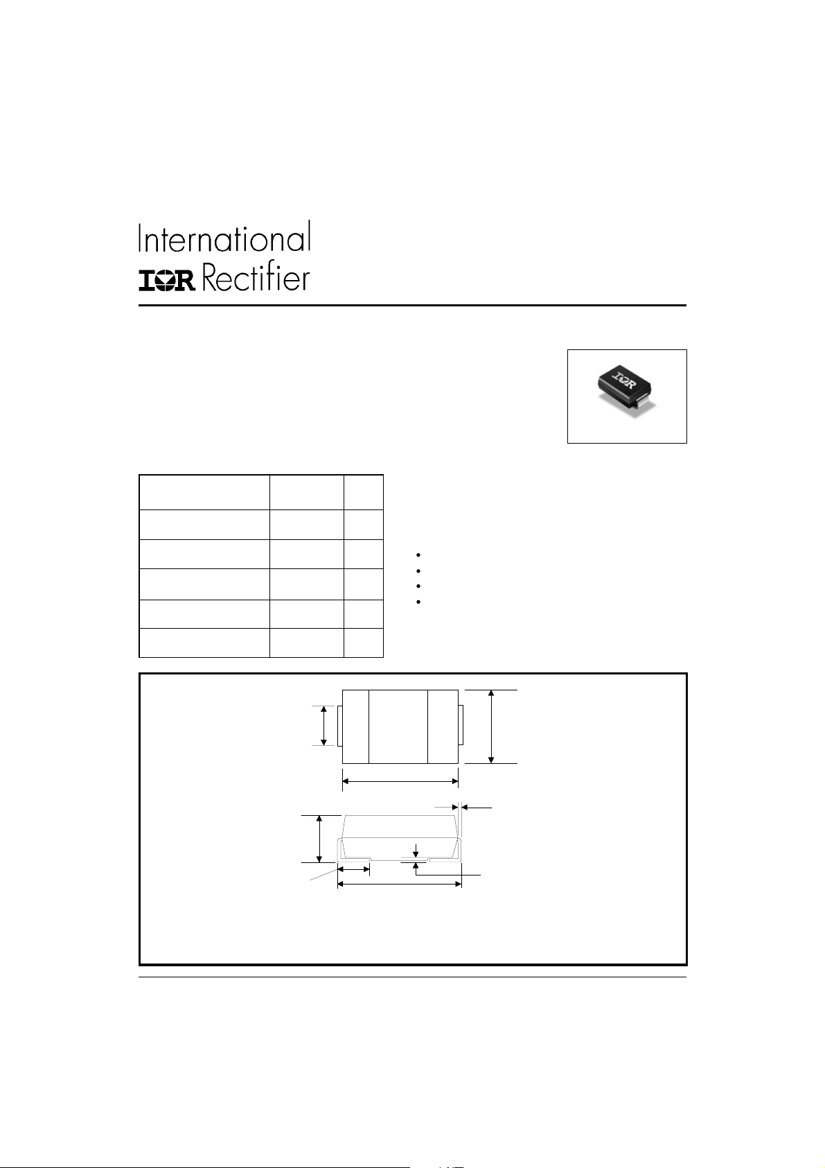
2.75 (.108)
3.15 (.124)
3 Amp
SMC
Description/Features
The MBRS340TR surface-mount Schottky rectifier has been
designed for applications requiring low forward drop and small
foot prints on PC boards. Typical applications are in disk drives,
switching power supplies, converters, free-wheeling diodes,
battery charging, and reverse battery protection.
Small foot print, surface mountable
Very low forward voltage drop
High frequency operation
Guard ring for enhanced ruggedness and long term
reliability
5.59 (.220)
6.22 (.245)
www.irf.com
6.60 (.260)
7.11 (.280)
2.00 (.079)
2.62 (.103)
0.76 (.030)
1.52 (.060)
Dimensions in millimeters and (inches)
For recommended footprint and soldering techniques refer to Application Note # AN-994
7.75 (.305)
8.13 (.320)
Outline SMC
.152 (.006)
.305 (.012)
.102 (.004)
.203 (.008)
1
Page 2
MBRS340TR
Bulletin PD-20585 04/01
Voltage Ratings
Part number MBRS340TR
VRMax. DC Reverse Voltage (V) 40
V
Max. Working Peak Reverse Voltage (V)
RWM
Absolute Maximum Ratings
Parameters Value Units Conditions
I
Max. Average Forward Current 3.0 A 50% duty cycle @ TL = 118 °C, rectangular wave form
F(AV)
4.0 50% duty cycle @ TL = 110 °C, rectangular wave form
I
Max. Peak One Cycle Non-Repetitive 1580 A 5µs Sine or 3µs Rect. pulse
FSM
Surge Current 80 10ms Sine or 6ms Rect. pulse
EASNon Repetitive Avalanche Energy 15 mJ TJ = 25 °C, IAS = 0.4A, L = 6.6mH
IARRepetitive Avalanche Current 0.4 A Current decaying linearly to zero in 1 µsec
Frequency limited by TJ max. Va = 1.5 x Vr typical
Following any rated
load condition and
with rated V
RRM
Electrical Specifications
Parameters Value Units Conditions
VFMMax. Forward Voltage Drop (1) 0.525 V @ 3A
0.68 V @ 6A
0.43 V @ 3A
0.57 V @ 6A
IRMMax. Reverse Leakage Current (1) 2.0 mA TJ = 25 °C
20 mA TJ = 100 °C
35 mA TJ = 125 °C
CTMax. Junction Capacitance 230 pF VR = 5VDC (test signal range 100KHz to 1Mhz) 25°C
LSTypical Series Inductance 3.0 nH Measured lead to lead 5mm from package body
dv/dt Max. Voltage Rate of Change 10000 V/µs
(Rated VR)
(1) Pulse Width < 300µs, Duty Cycle < 2%
TJ = 25 °C
TJ = 125 °C
VR = rated V
R
applied
Thermal-Mechanical Specifications
Parameters Value Units Conditions
TJMax. Junction Temperature Range - 55 to 150 °C
T
Max. Storage Temperature Range - 55 to 150 °C
stg
R
Max. Thermal Resistance, Junction 12 °C/W DC Operation (* See Fig. 4)
thJL
to Lead (2)
wt Approximate Weight 0.24 g
Case Style SMCSimilar DO-214AB
(2) Mounted 1 inch square PCB, Thermal Probe connected to lead 2mm from Package
2
www.irf.com
Page 3

MBRS340TR
Bulletin PD-20585 04/01
10
(A)
F
1
Instantaneous Forward Current - I
T = 150˚C
J
T = 125˚C
J
T = 25˚C
J
100000
(mA)
R
Reverse Current - I
T = 150˚C
J
10000
1000
100
10
125˚C
100˚C
75˚C
50˚C
25˚C
1
0 10203040
Reverse Voltage - VR (V)
Fig. 2 - Typical Values Of Reverse Current
Vs. Reverse Voltage (Per Leg)
1000
T = 25˚C
J
(p F)
T
100
0.1
0 0.1 0.2 0.3 0.4 0.5 0.6 0.7 0.8 0.9
Fig. 1 - Max. Forward Voltage Drop Characteristics
www.irf.com
Junction Capacitance - C
10
Forward Voltage Drop - VFM (V)
0 5 10 15 20 25 30 35 40 45
Reverse Voltage - VR (V)
Fig. 3 - Typical Junction Capacitance
(Per Leg)
Vs. Reverse Voltage (Per Leg)
100
(°C/W)
Thermal Impedance Z
D = 0.75
10
D = 0.50
thJC
D = 0.33
D = 0.25
D = 0.20
1
Single Pulse
(Thermal Resistance)
0.1
0.00001 0.0001 0.001 0.01 0.1 1 10 100
Notes:
1. Duty factor D = t1/ t 2
2. Peak Tj = Pdm x ZthJC+Tc
P
DM
t
1
t
2
t1 , Rectangular Pulse Duration (Seconds)
Fig. 4 - Max. Thermal Impedance Z
Characteristics (Per Leg)
thJC
3
Page 4

MBRS340TR
Bulletin PD-20585 04/01
160
150
DC
140
130
120
110
100
Square wave (D = 0.50)
90
Rated Vr applied
80
Allowable Lead Temperature (°C)
70
see note (2)
60
012345
Average Forward Current - I
Fig. 4 - Maximum Average Forward Current
Vs. Allowable Lead Temperature
1000
(A)
FSM
100
D=0.20
D=0.25
D=0.33
D=0.50
D=0.75
F(AV)
(A)
2
D = 0.20
D = 0.25
D = 0.33
D = 0.50
1.5
D = 0.75
DC
RMS Limit
1
0.5
Average Power Loss (Watts)
0
0 0.5 1 1.5 2 2.5 3 3.5 4 4.5
Average Forward Current - I
Fig. 5 - Maximum Average Forward Dissipation
Vs. Average Forward Current
F(AV)
(A)
Fig. 6 - Maximum Peak Surge Forward Current Vs. Pulse Duration
(2) Formula used: TC = TJ - (Pd + Pd
Pd = Forward Power Loss = I
Pd
= Inverse Power Loss = VR1 x IR (1 - D); IR @ V
REV
F(AV)
4
At Any Rated Load Condition
And With rated Vrrm Applied
Following Surge
Non-Repetitive Surge Current - I
10
10 100 1000 10000
Square Wave Pulse Duration - T
) x R
REV
x VFM @ (I
;
thJC
/ D) (see Fig. 6);
F(AV)
= 80% rated V
R1
R
(Microsec)
p
www.irf.com
Page 5

Tape & Reel Information
MBRS340TR
Bulletin PD-20585 04/01
330 (13)
16 (0.63)
Dimensions in millimeters and (inches)
Marking & Identification
Each device has marking and identification on two rows.
- The first row designates the device as manufactured by
International Rectifier as indicated by the letters "IR", then
Current and Voltage.
- The second row shows the data code: Year and Week.
See below marking diagram.
FIRST ROW
IR 3 4
SECOND ROW
Date Code
Y Y W W
16 (0.63)
8 (0.32)
FEED DIRECTION
Ordering Information
MBRS340TR - TAPE AND REEL
WHEN ORDERING, INDICATE THE PART NUMBER
AND THE QUANTITY ( IN MULTIPLES OF 3000
PIECES).
EXAMPLE: MBRS340TR - 6000 PIECES
www.irf.com
5
Page 6

MBRS340TR
Bulletin PD-20585 04/01
Data and specifications subject to change without notice.
This product has been designed and qualified for Industrial Level.
Qualification Standards can be found on IR's Web site.
IR WORLD HEADQUARTERS: 233 Kansas St., El Segundo, California 90245, USA Tel: (310) 252-7105
TAC Fax: (310) 252-7309
Visit us at www.irf.com for sales contact information. 04/01
6
www.irf.com
 Loading...