

Page 1
August 1999
LPV321 Single/ LPV358 Dual/ LPV324 Quad
General Purpose, Low Voltage, Low Power, Rail-to-Rail
Output Operational Amplifiers
LPV321 Single/ LPV358 Dual/ LPV324 Quad General Purpose, Low Voltage, Low Power,
Rail-to-Rail Output Operational Amplifiers
General Description
The LPV321/358/324 are low power (9µA per channel at
5.0V) versions of the LMV321/358/324 op amps. This is another addition to the LMV321/358/324 family of commodity
op amps.
The LPV321/358/324 are the most cost effective solutions
for the applications where low voltage, low poweroperation,
space saving and low price are needed. The
LPV321/358/324 have rail-to-rail output swing capability and
the input common-mode voltage range includes ground.
They all exhibit excellent speed-power ratio, achieving
152 KHz of bandwidth with a supply current of only 9µA.
The LPV321 is available in space saving SC70-5, which is
approximately half the size of SOT23-5. The small package
saves space on pc boards, and enables the design of small
portable electronic devices. It also allows the designer to
place the device closer to the signal source to reduce noise
pickup and increase signal integrity.
The chips are built with National’s advanced submicron
silicon-gate BiCMOS process. The LPV321/358/324 have bipolar input and output stages for improved noise performance and higher output current drive.
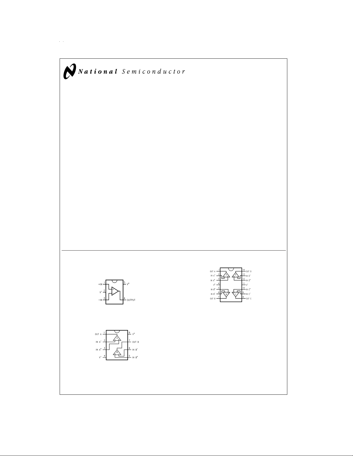
Connection Diagrams
5-Pin
SC70-5/SOT23-5
Features
+
=
(For V
j
Guaranteed 2.7V and 5V Performance
j
No Crossover Distortion
j
Space Saving Package SC70-5
j
Industrial Temp.Range −40˚C to +85˚C
j
Gain-Bandwidth Product 152KHz
j
Low Supply Current
LPV321 9µA
LPV358 15µA
LPV324 28µA
j
Rail-to-Rail Output Swing
@
100kΩ Load V+−3.5mV
j
V
CM
5V and V
−
=
0V,TypicalUnless Otherwise Noted)
2.0x2.1x1.0mm
−
V
−0.2V to V+−0.8V
Applications
n Active Filters
n General Purpose Low Voltage Applications
n General Purpose Portable Devices
14-Pin SO/TSSOP
+90mV
DS100920-1
Top View
8-Pin SO/MSOP
DS100920-2
Top View
© 1999 National Semiconductor Corporation DS100920 www.national.com
DS100920-3
Top View
Page 2
Ordering Information
Temperature Range
Package
−40˚C to +85˚C
5-Pin SC70-5 LPV321M7 A19 1k Units Tape and Reel MAA05
LPV321M7X A19 3k Units Tape and Reel
5-Pin SOT23-5 LPV321M5 A27A 1k Units Tape and Reel MA05B
LPV321M5X A27A 3k Units Tape and Reel
8-Pin Small Outline LPV358M LPV358M Rails
LPV358MX LPV358M 2.5k Units Tape and Reel
8-Pin MSOP LPV358MM P358 1k Units Tape and Reel
LPV358MMX P358 3.5k Units Tape and Reel
14-Pin Small Outline LPV324M LPV324M Rails
LPV324MX LPV324M 2.5k Units Tape and Reel
14-Pin TSSOP LPV324MT LPV324MT Rails
LPV324MTX LPV324MT 2.5k Units Tape and Reel
Packaging Marking Transport Media NSC DrawingIndustrial
M08A
MUA08A
M14A
MTC14
www.national.com 2
Page 3
Absolute Maximum Ratings (Note 1)
If Military/Aerospace specified devices are required,
please contact the National Semiconductor Sales Office/
Distributors for availability and specifications.
ESD Tolerance (Note 2)
Machine Model 100V
Human Body Model 2000V
Differential Input Voltage
Supply Voltage (V
Output Short Circuit to V
Output Short Circuit to V
+–V−
) 5.5V
+
−
Soldering Information
Infrared or Convection (20 sec) 235˚C
Storage Temp. Range −65˚C to 150˚C
±
Supply Voltage
(Note 3)
(Note 4)
Junction Temp. (T
, max) (Note 5) 150˚C
j
Operating Ratings (Note 1)
Supply Voltage 2.7V to 5V
Temperature Range −40˚C≤T
Thermal Resistance (θ
)(Note 10)
JA
5-pin SC70-5 478˚C/W
5-pin SOT23-5 265˚C/W
8-Pin SOIC 190˚C/W
8-Pin MSOP 235˚C/W
14-Pin SOIC 145˚C/W
14-Pin TSSOP 155˚C/W
≤85˚C
J
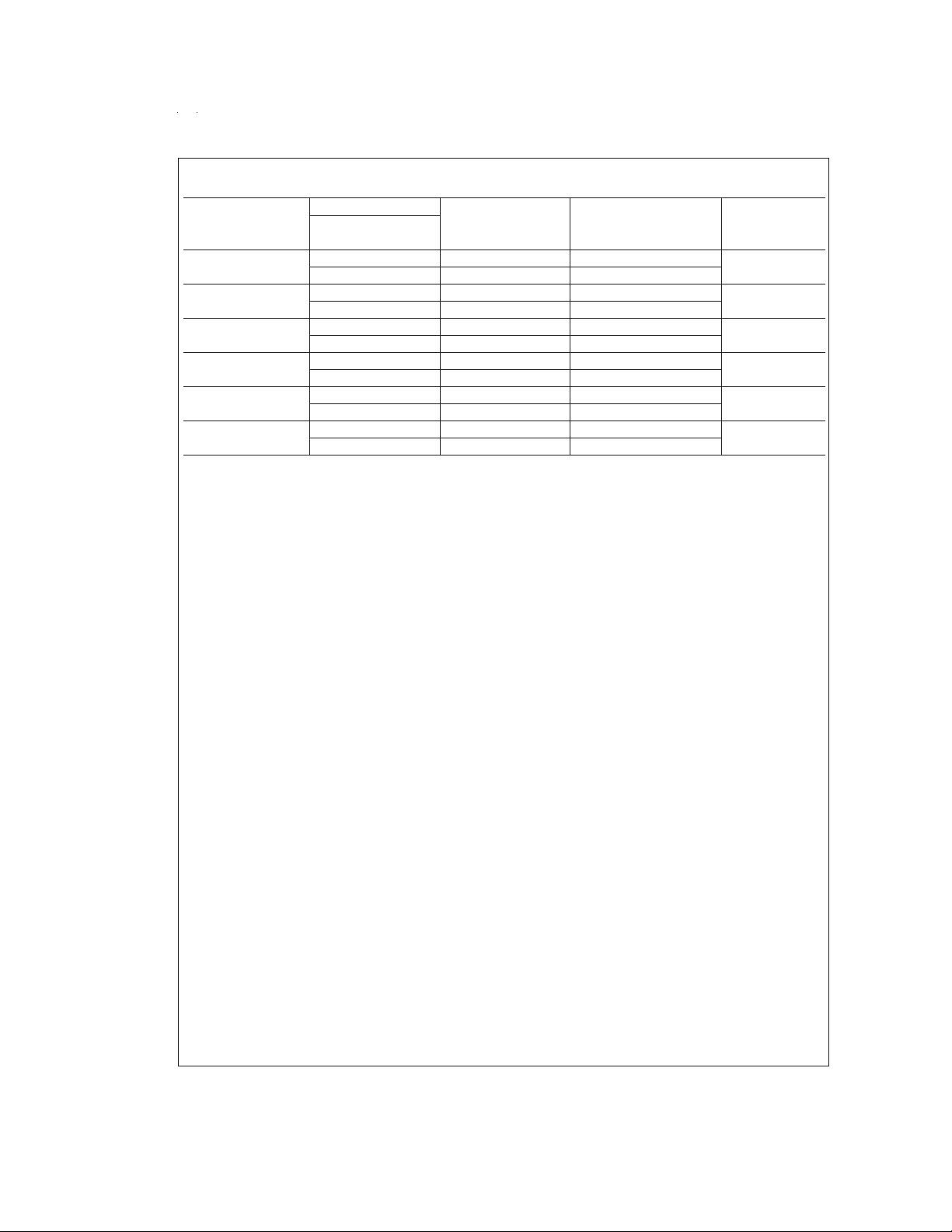
2.7V DC Electrical Characteristics
Unless otherwise specified, all limits guaranteed for TJ= 25˚C, V+= 2.7V, V−= 0V, VCM= 1.0V, VO=V+/2 and R
Symbol Parameter Conditions
V
OS
TCV
I
B
I
OS
CMRR Common Mode Rejection Ratio 0V ≤ V
PSRR Power Supply Rejection Ratio 2.7V ≤ V
V
CM
V
O
I
S
Input Offset Voltage 1.2 7 mV
Input Offset Voltage Average
OS
Drift
Input Bias Current 1.7 50 nA
Input Offset Current 0.6 40 nA
≤ 1.7V 70 50 dB
CM
+
≤ 5V
Input Common-Mode Voltage
=
V
O
For CMRR ≥ 50dB −0.2 0 V
1V, V
=
1V
CM
Range
Output Swing RL= 100kΩ to 1.35V V+-3 V+-100 mV
Supply Current LPV321 4 8 µA
LPV358
Both amplifiers
LPV324
All four amplifiers
Typ
(Note 6)
2 µV/˚C
65 50 dB
1.9 1.7 V
80 180 mV
816µA
16 24 µA
Limit
(Note 7) Units
L
>
1MΩ.
max
max
max
min
min
min
max
min
max
max
max
max
www.national.com3
Page 4
2.7V AC Electrical Characteristics
Unless otherwise specified, all limits guaranteed for TJ= 25˚C, V+= 2.7V, V−= 0V, VCM= 1.0V, VO=V+/2 and R
Symbol Parameter Conditions
GBWP Gain-Bandwidth Product C
Φ
m
G
m
e
n
Phase Margin 97 Deg
Gain Margin 35 dB
Input-Referred Voltage Noise f = 1 kHz 178
= 22 pF 112 KHz
L
Typ
(Note 6)
Limit
(Note 7)
L
>
1MΩ.
Units
i
n
Input-Referred Current Noise f = 1 kHz 0.50
5V DC Electrical Characteristics
Unless otherwise specified, all limits guaranteed for TJ= 25˚C, V+= 5V, V−= 0V, VCM= 2.0V, VO=V+/2 and R
Boldface limits apply at the temperature extremes.
Symbol Parameter Conditions
V
OS
TCV
I
B
I
OS
CMRR Common Mode Rejection Ratio 0V ≤ V
PSRR Power Supply Rejection Ratio 2.7V ≤ V
V
CM
A
V
V
O
I
O
I
S
Input Offset Voltage 1.5 7
Input Offset Voltage Average
OS
Drift
Input Bias Current 2 50
Input Offset Current 0.6 40
≤ 4V 71 50 dB
CM
+
≤ 5V
Input Common-Mode Voltage
=
V
O
For CMRR ≥ 50dB −0.2 0 V
1V, V
=
1V
CM
Range
Large Signal Voltage Gain
RL= 100kΩ 100 15
(Note 8)
Output Swing RL= 100kΩ to 2.5V V+−3.5 V+−100
Output Short Circuit Current Sourcing, VO=0V 17 2 mA
Sinking, V
=5V 72 20 mA
O
Supply Current LPV321 9 12
LPV358
Both amplifiers
LPV324
All four amplifiers
Typ
(Note 6)
2 µV/˚C
65 50 dB
4.2 4 V
90 180
15 20
28 42
Limit
(Note 7)
10
60
50
10
+
−200
V
220
15
24
46
L
>
1MΩ.
Units
mV
max
nA
max
nA
max
min
min
min
max
V/mV
min
mV
min
mV
max
min
min
µA
max
µA
max
µA
max
www.national.com 4
Page 5
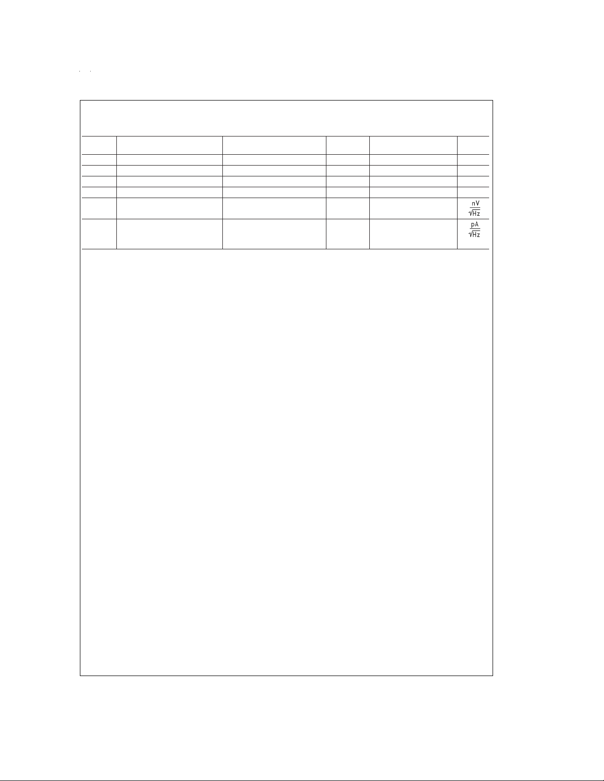
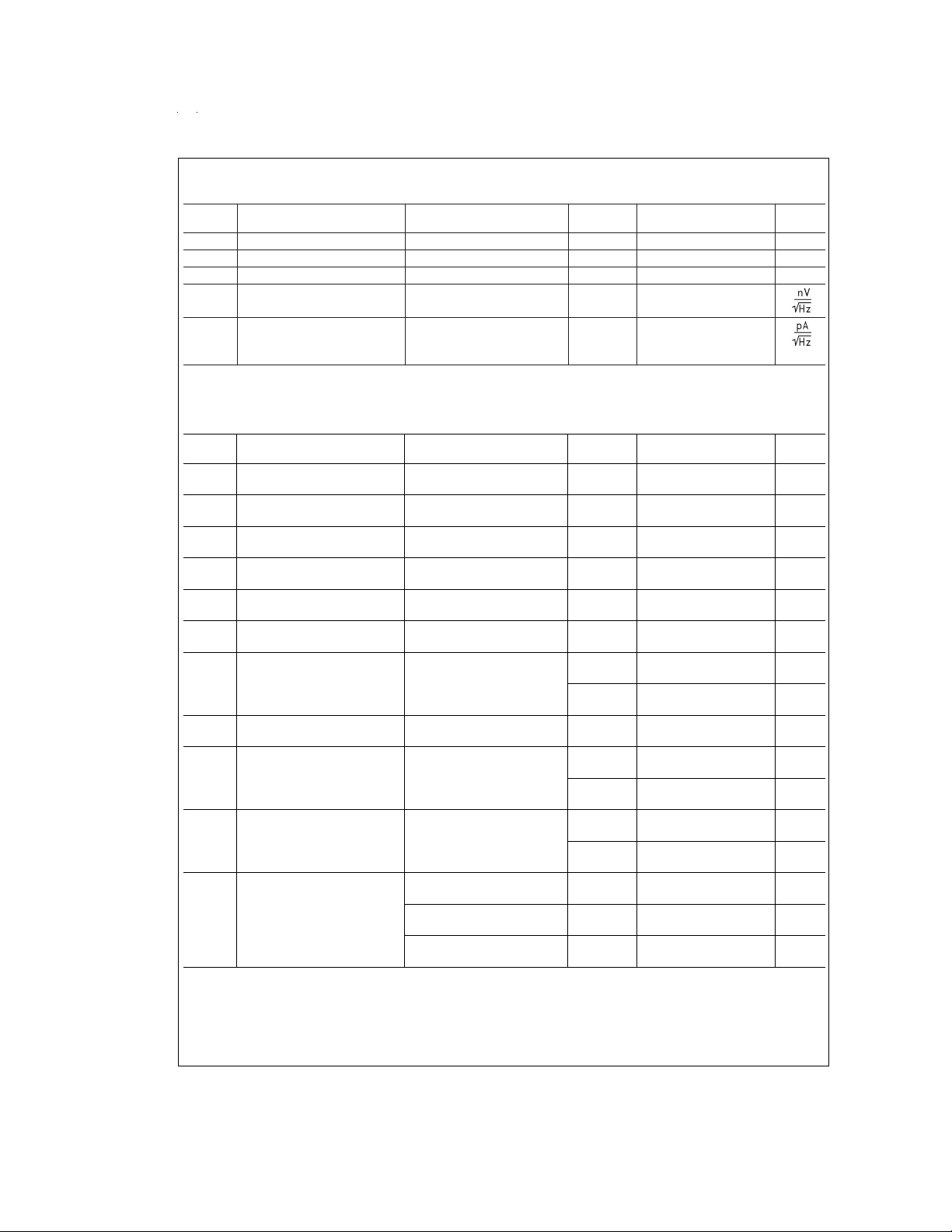
5V AC Electrical Characteristics
Unless otherwise specified, all limits guaranteed for TJ= 25˚C, V+= 5V, V−= 0V, VCM= 2.0V, VO=V+/2 and R
Boldface limits apply at the temperature extremes.
Symbol Parameter Conditions
Typ
(Note 6)
Limit
(Note 7)
SR Slew Rate (Note 9) 0.1 V/µs
GBWP Gain-Bandwidth Product C
Φ
m
G
m
e
n
Phase Margin 87 Deg
Gain Margin 19 dB
Input-Referred Voltage Noise f = 1 kHz, 146
= 22 pF 152 KHz
L
L
>
1MΩ.
Units
i
n
Note 1: Absolute Maximum Ratings indicate limits beyond which damage to the device may occur. Operating Ratings indicate conditions for which the device is intended to be functional, but specific performance is not guaranteed. For guaranteed specifications and the test conditions, see the Electrical Characteristics.
Note 2: Human body model, 1.5 kΩ in series with 100 pF. Machine model, 0Ω in series with 200 pF.
Note 3: Shorting output to V
Note 4: Shorting output to V
Note 5: The maximum power dissipation is a function of T
P
Note 6: Typical values represent the most likely parametric norm.
Note 7: All limits are guaranteed by testing or statistical analysis.
Note 8: R
Note 9: Connected as voltage follower with 3V step input. Number specified is the slower of the positive and negative slew rates.
Note 10: All numbers are typical, and apply for packages soldered directly onto a PC board in still air.
Input-Referred Current Noise f = 1 kHz 0.30
+
will adversely affect reliability.
-
will adversely affect reliability.
=(T
D
)/θJA. All numbers apply for packages soldered directly into a PC board.
J(max)–TA
is connected to V-. The output voltage is 0.5V ≤ VO≤ 4.5V.
L
, θJA, and TA. The maximum allowable power dissipation at any ambient temperature is
J(max)
www.national.com5
Page 6
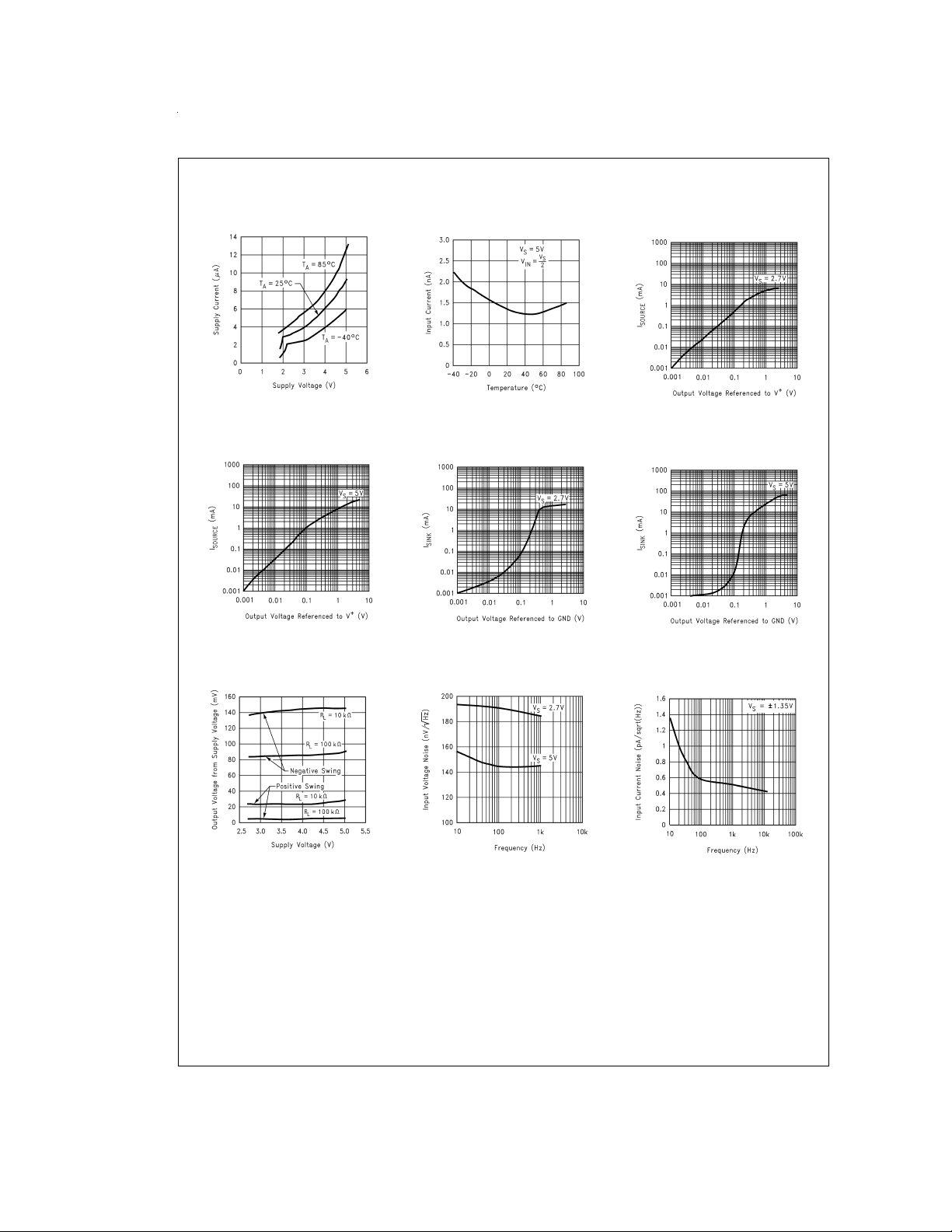
Typical Performance Characteristics Unless otherwise specified, V
Supply Current vs Supply
Voltage (LPV321)
Input Current vs
Temperature
Sourcing Current vs
Output Voltage
= +5V, single supply, TA= 25˚C.
S
Sourcing Current vs
Output Voltage
Output Voltage Swing vs
Supply Voltage
DS100920-B4
DS100920-42
Sinking Current vs
Output Voltage
Input Voltage Noise vs
Frequency
DS100920-B5
DS100920-43
DS100920-41
Sinking Current vs
Output Voltage
DS100920-44
Input Current Noise vs
Frequency
DS100920-B6
www.national.com 6
DS100920-56
DS100920-70
Page 7
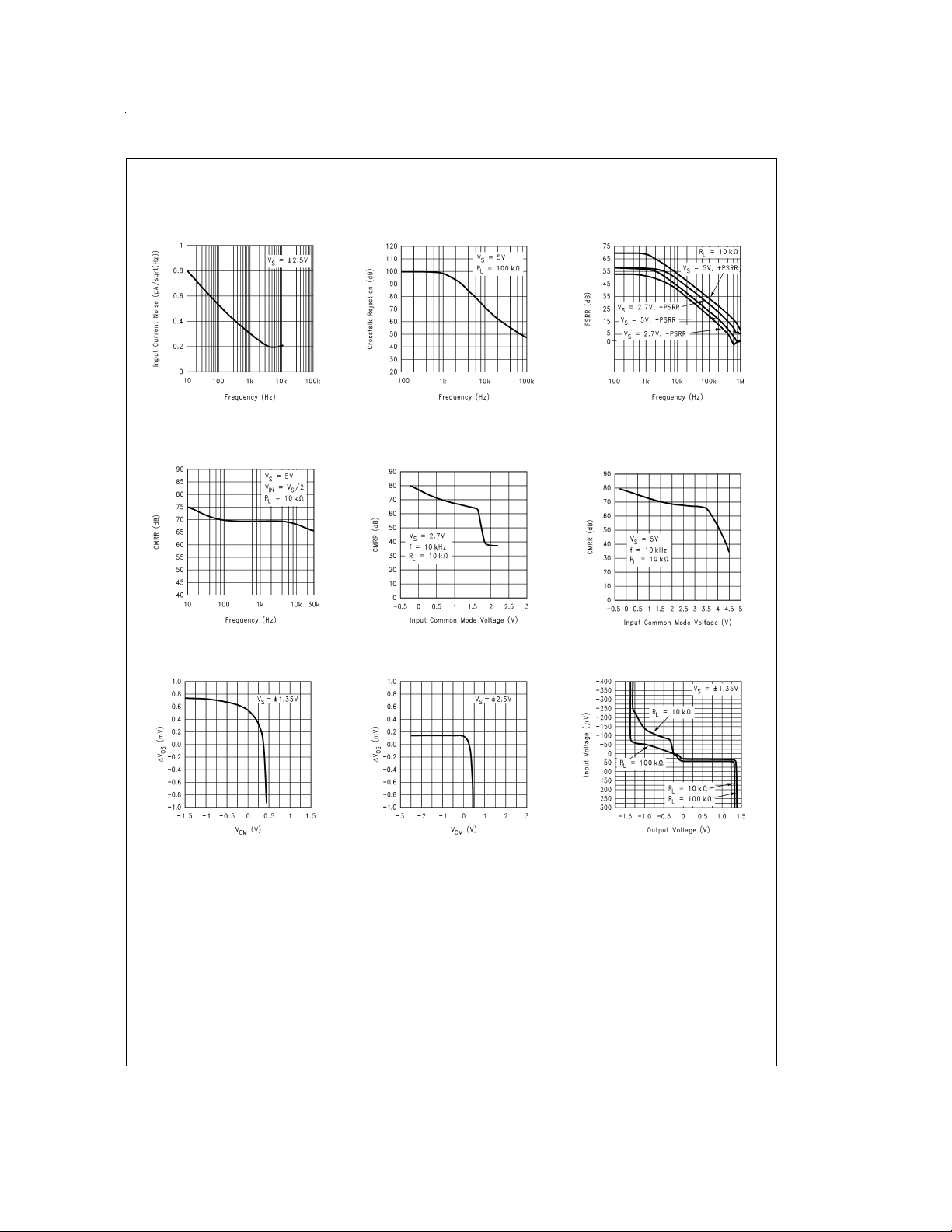
Typical Performance Characteristics Unless otherwise specified, V
T
= 25˚C. (Continued)
A
= +5V, single supply,
S
Input Current Noise vs Frequency
DS100920-68
CMRR vs
Frequency
DS100920-63
∆VOSvs CMR
Crosstalk Rejection vs Frequency
DS100920-73
CMRR vs Input
Common Mode Voltage
DS100920-64
∆VOSvs CMR
PSRR vs Frequency
DS100920-72
CMRR vs Input
Common Mode Voltage
DS100920-65
Input Voltage vs Output Voltage
DS100920-45
DS100920-46
DS100920-69
www.national.com7
Page 8

Typical Performance Characteristics Unless otherwise specified, V
T
= 25˚C. (Continued)
A
= +5V, single supply,
S
Input Voltage vs
Output Voltage
Gain and Phase vs
Capacitive Load
DS100920-71
DS100920-54
Open Loop
Frequency Response
Gain and Phase vs
Capacitive Load
DS100920-52
DS100920-53
Open Loop
Frequency Response
DS100920-51
Slew Rate vs
Supply Voltage
DS100920-55
Non-Inverting Large
Signal Pulse Response
DS100920-50
www.national.com 8
Non-Inverting Small
Signal Pulse Response
DS100920-49
Inverting Large Signal
Pulse Response
DS100920-47
Page 9

Typical Performance Characteristics Unless otherwise specified, V
T
= 25˚C. (Continued)
A
= +5V, single supply,
S
Inverting Small Signal
Pulse Response
Stability vs Capacitive Load
Open Loop Output
Impedance vs Frequency
DS100920-48
DS100920-59
Stability vs Capacitive Load
Stability vs Capacitive Load
Short Circuit Current
vs Temperature (Sinking)
DS100920-61
DS100920-58
Stability vs Capacitive Load
DS100920-60
THD vs Frequency
DS100920-62
Short Circuit Current
vs Temperature (Sourcing)
DS100920-74
Application Notes
1.0 Benefits of the LPV321/358/324
Size. The small footprints of the LPV321/358/324 packages
save space on printed circuit boards, and enable the design
of smaller electronic products, such as cellular phones, pagers, or other portable systems. The low profile of the
LPV321/358/324 make them possible to use in PCMCIA
type III cards.
Signal Integrity. Signals can pick up noise between the signal source and the amplifier. By using a physically smaller
DS100920-B7
DS100920-B8
amplifier package, the LPV321/358/324 can be placed
closer to the signal source, reducing noise pickup and increasing signal integrity.
Simplified Board Layout. These products help you to avoid
using long pc traces in your pc board layout. This means that
no additional components, such as capacitors and resistors,
are needed to filter out the unwanted signals due to the interference between the long pc traces.
Low Supply Current. These devices will help you to maximize battery life. They are ideal for battery powered systems.
www.national.com9
Page 10

Application Notes (Continued)
Low Supply Voltage. National provides guaranteed perfor-
mance at 2.7V and 5V. These guarantees ensure operation
throughout the battery lifetime.
Rail-to-Rail Output. Rail-to-rail output swing provides maximum possible dynamic range at the output. This is particularly important when operating on low supply voltages.
Input Includes Ground. Allows direct sensing near GND in
single supply operation.
The differential input voltage may be larger than V
damaging the device. Protection should be provided to prevent the input voltages from going negative more than −0.3V
(at 25˚C). An input clamp diode with a resistor to the IC input
terminal can be used.
2.0 Capacitive Load Tolerance
The LPV321/358/324 can directly drive 200 pF in unity-gain
without oscillation. The unity-gain follower is the most sensitive configuration to capacitive loading. Direct capacitive
loading reduces the phase margin of amplifiers. The combination of the amplifier’s output impedance and the capacitive
load induces phase lag. This results in either an underdamped pulse response or oscillation. Todrive a heavier capacitive load, circuit in
Figure 1
can be used.
+
without
ing the value of R
LPV321/358/324. C
of phase margin by feeding the high frequency component of
due to the input bias current of the
F
F
and R
serve to counteract the loss
ISO
the output signal back to the amplifier’s inverting input,
thereby preserving phase margin in the overall feedback
loop. Increased capacitive drive is possible by increasing the
value of C
. This in turn will slow down the pulse response.
F
DS100920-5
FIGURE 3. Indirectly Driving A Capacitive Load with
DC Accuracy
3.0 Input Bias Current Cancellation
The LPV321/358/324 family has a bipolar input stage. The
typical input bias current of LPV321/358/324 is 1.5nA with
5V supply. Thus a 100kΩ input resistor will cause 0.15mV of
error voltage. By balancing the resistor values at both inverting and non-inverting inputs, the error caused by the amplifier’s input bias current will be reduced. The circuit in
4
shows how to cancel the error caused by input bias
Figure
current.
DS100920-4
FIGURE 1. Indirectly Driving A Capacitive Load Using
Resistive Isolation
Figure 1
In
C
margin to the overall system. The desired performance depends on the value of R
value, the more stable V
waveform of
C
, the isolation resistor R
form a pole to increase stability by adding more phase
L
ISO
.
Figure 1
L
OUT
using 100kΩ for R
and the load capacitor
ISO
. The bigger the R
will be.
Figure 2
and 1000pF for
ISO
DS100920-75
resistor
ISO
is an output
FIGURE 2. Pulse Response of the LPV324 Circuit in
Figure 1
Figure 3
The circuit in
1
because it provides DC accuracy as well as AC stability. If
there were a load resistor in
voltage divided by R
ure 3
,RFprovides the DC accuracy by using feed-forward
techniques to connect V
www.national.com 10
is an improvement to the one in
Figure 1
and the load resistor. Instead, in
ISO
to RL. Caution is needed in choos-
IN
, the output would be
Figure
Fig-
DS100920-6
FIGURE 4. Cancelling the Error Caused by Input Bias
Current
4.0 Typical Single-Supply Application Circuits
4.1 Difference Amplifier
The difference amplifier allows the subtraction of two voltages or, as a special case, the cancellation of a signal common to two inputs. It is useful as a computational amplifier,in
making a differential to single-ended conversion or in rejecting a common mode signal.
Page 11

Application Notes (Continued)
DS100920-7
FIGURE 5. Difference Amplifier
4.2 Instrumentation Circuits
The input impedance of the previous difference amplifier is
set by the resistor R
lems of low input impedance, one way is to use a voltage follower ahead of each input as shown in the following two instrumentation amplifiers.
4.2.1Three-op-amp Instrumentation Amplifier
The quad LPV324 can be used to build a three-op-amp instrumentation amplifier as shown in
, and R4. Toeliminate the prob-
1,R2,R3
Figure 6
4.2.2 Two-op-amp Instrumentation Amplifier
A two-op-amp instrumentation amplifier can also be used to
make a high-input-impedance DC differential amplifier (
ure 7
). As in the three-op-amp circuit, this instrumentation
Fig-
amplifier requires precise resistor matching for good CMRR.
R
should equal to R1and R3should equal R2.
4
DS100920-11
FIGURE 7. Two-op-amp Instrumentation Amplifier
4.3 Single-Supply Inverting Amplifier
There may be cases where the input signal going into the
amplifier is negative. Because the amplifier is operating in
single supply voltage, a voltage divider using R
implemented to bias the amplifier so the input signal is within
and R4is
3
the input common-common voltage range of the amplifier.
The capacitor C
resistor R
source, V
quency, fc=1/2π R
As a result, the ouptut signal is centered around mid-supply
(if the voltage divider provides V
is placed between the inverting input and
1
to block the DC signal going into the AC signal
1
. The values of R1and C1affect the cutoff fre-
IN
1C1
.
+
/2 at the non-inverting input). The output can swing to both rails, maximizing the
signal-to-noise ratio in a low voltage system.
DS100920-85
FIGURE 6. Three-op-amp Instrumentation Amplifier
The first stage of this instrumentation amplifier is a
differential-input, differential-output amplifier, with two voltage followers. These two voltage followers assure that the
input impedance is over 100MΩ. The gain of this instrumentation amplifier is set by the ratio of R
R
and R4equal R2. Matching of R3to R1and R4to R2af-
1
fects the CMRR. For good CMRR over temperature, low drift
resistors should be used. Making R
2
and adding a trim pot equal to twice the difference between
R
and R4will allow the CMRR to be adjusted for optimum.
2
Slightly smaller than R
4
2/R1.R3
should equal
DS100920-13
FIGURE 8. Single-Supply Inverting Amplifier
4.4 Active Filter
4.4.1 Simple Low-Pass Active Filter
Figure 9
The simple low-pass filter is shown in
low-frequency gain(ω→o) is defined by −R
low-frequency gains other than unity to be obtained. The fil-
3/R1
. Its
. This allows
ter has a −20dB/decade roll-off after its corner frequency fc.
R
should be chosen equal to the parallel combination of R
2
and R3to minimize errors due to bais current. The frequency
response of the filter is shown in
Figure 10
www.national.com11
1
Page 12

Application Notes (Continued)
FIGURE 9. Simple Low-Pass Active Filter
DS100920-14
DS100920-15
FIGURE 10. Frequency Response of Simple Low-pass
Active Filter in Figure 9
Note that the single-op-amp active filters are used in to the
applications that require low quality factor, Q (≤ 10), low frequency (≤ 5KHz), and low gain (≤ 10), or a small value for the
product of gain times Q (≤ 100). The op amp should have an
open loop voltage gain at the highest frequency of interest at
least 50 times larger than the gain of the filter at this frequency.In addition, the selected op amp should have a slew
rate that meets the following requirement:
SlewRate ≥ 0.5x(ω
Where ω
the output peak-to-peak voltage.
www.national.com 12
is the highest frequency of interest, and V
H
HVOPP
)X10−6V/µsec
OPP
is
Page 13

SC70-5 Tape and Reel Specification
SOT-23-5 Tape and Reel Specification
TAPE FORMAT
Tape Section
Leader 0 (min) Empty Sealed
(Start End) 75 (min) Empty Sealed
Carrier 3000 Filled Sealed
Trailer 125 (min) Empty Sealed
(Hub End) 0 (min) Empty Sealed
#
Cavities Cavity Status Cover Tape Status
250 Filled Sealed
DS100920-B3
www.national.com13
Page 14

SOT-23-5 Tape and Reel Specification (Continued)
TAPE DIMENSIONS
DS100920-B1
8 mm 0.130 0.124 0.130 0.126 0.138±0.002 0.055±0.004 0.157 0.315±0.012
(3.3) (3.15) (3.3) (3.2) (3.5
Tape Size DIM A DIM Ao DIM B DIM Bo DIM F DIM Ko DIM P1 DIM W
www.national.com 14
±
0.05) (1.4±0.11) (4) (8±0.3)
Page 15

SOT-23-5 Tape and Reel Specification (Continued)
REEL DIMENSIONS
8 mm 7.00 0.059 0.512 0.795 2.165 0.331 + 0.059/−0.000 0.567 W1+ 0.078/−0.039
330.00 1.50 13.00 20.20 55.00 8.40 + 1.50/−0.00 14.40 W1 + 2.00/−1.00
Tape Size A B C D N W1 W2 W3
DS100920-B2
www.national.com15
Page 16

Physical Dimensions inches (millimeters) unless otherwise noted
5-Pin SC70-5 Tape and Reel
Order Number LPV321M7 and LPV321M7X
NS Package Number MAA05A
www.national.com 16
Page 17

Physical Dimensions inches (millimeters) unless otherwise noted (Continued)
5-Pin SOT23-5 Tape and Reel
Order Number LPV321M5 and LPV321M5X
NS Package Number MA05B
www.national.com17
Page 18

Physical Dimensions inches (millimeters) unless otherwise noted (Continued)
Order Number LPV358M and LPV358MX
8-Pin Small Outline
NS Package Number M08A
www.national.com 18
Page 19

Physical Dimensions inches (millimeters) unless otherwise noted (Continued)
Order Number LPV358MM and LPV358MMX
8-Pin MSOP
NS Package Number MUA08A
www.national.com19
Page 20

Physical Dimensions inches (millimeters) unless otherwise noted (Continued)
Order Number LPV324M and LPV324MX
14-Pin Small Outline
NS Package Number M14A
www.national.com 20
Page 21

Physical Dimensions inches (millimeters) unless otherwise noted (Continued)
LPV321 Single/ LPV358 Dual/ LPV324 Quad General Purpose, Low Voltage, Low Power,
Rail-to-Rail Output Operational Amplifiers
Order Number LPV324MT and LPV324MTX
14-Pin TSSOP
NS Package Number MTC14
LIFE SUPPORT POLICY
NATIONAL’S PRODUCTS ARE NOT AUTHORIZED FOR USE AS CRITICAL COMPONENTS IN LIFE SUPPORT
DEVICES OR SYSTEMS WITHOUT THE EXPRESS WRITTEN APPROVAL OF THE PRESIDENT AND GENERAL
COUNSEL OF NATIONAL SEMICONDUCTOR CORPORATION. As used herein:
1. Life support devices or systems are devices or
systems which, (a) are intended for surgical implant
into the body, or (b) support or sustain life, and
whose failure to perform when properly used in
accordance with instructions for use provided in the
2. A critical component is any component of a life
support device or system whose failure to perform
can be reasonably expected to cause the failure of
the life support device or system, or to affect its
safety or effectiveness.
labeling, can be reasonably expected to result in a
significant injury to the user.
National Semiconductor
Corporation
Americas
Tel: 1-800-272-9959
Fax: 1-800-737-7018
Email: support@nsc.com
www.national.com
National does not assume any responsibility for use of any circuitry described, no circuit patent licenses are implied and National reserves the right at any time without notice to change said circuitry and specifications.
National Semiconductor
Europe
Fax: +49 (0) 1 80-530 85 86
Email: europe.support@nsc.com
Deutsch Tel: +49 (0) 1 80-530 85 85
English Tel: +49 (0) 1 80-532 78 32
Français Tel: +49 (0) 1 80-532 93 58
Italiano Tel: +49 (0) 1 80-534 16 80
National Semiconductor
Asia Pacific Customer
Response Group
Tel: 65-2544466
Fax: 65-2504466
Email: sea.support@nsc.com
National Semiconductor
Japan Ltd.
Tel: 81-3-5639-7560
Fax: 81-3-5639-7507
 Loading...