

Page 1
现货库存、技术资料、百科信息、热点资讯,精彩尽在鼎好!
1
2
3
45
6
7
8
-
+
-
+
LOW POWER DUAL OPERATIONAL AMPLIFIERS
LM158,A-LM258,A
LM358,A
■ INTERNALLY FREQUENCY COMPENSATED
■ LARGE DC VOLTAGE GAIN : 1 00d B
■ WIDE BANDWIDTH (unity gain): 1.1MHz
(temperature compensated)
■ VERY LOW SUPPLY CURRENT/OP (500µA)
ESSENTIALLY IN DEPENDENT OF SUPPLY
VOLT AGE
■ LOW INPUT BIAS CURRENT: 20nA
(temperature compensated)
■ LOW INPUT OFFSET VOLTAGE: 2mV
■ LOW INPUT OFFSET CURRENT: 2nA
■ INPUT COMMON - MO DE VOLTAGE RANGE
INCLUDES GROUND
■ DIFFERENTIAL INPUT VOLTAGE RANGE
EQUA L TO T H E P O W ER SUPPLY VOLTAG E
■ LARGE OUTPUT VOLTAGE SWING 0V TO
(Vcc - 1.5V)
DESCRIPTION
These circuits consist of two independent, high
gain, internally frequency compensated which
were designed specifically to ope rate from a single power supply over a wide range of vol tages.
The low power supply drain is independent of the
magnitude of the power supply voltage.
Application areas include transducer amplifiers,
dc gain blocks and all the conventional op-amp
circuits which now can be more easily implemented in single power supply systems. For example,
these circuits can be directly supplied with the
standard +5V which is used in logic system s and
will easily provide the requir ed interface electronics without requiring any additional power supply.
Inthe linear mode the input common-mode voltage
range includes ground and the output voltage can
also swing to ground, even though op erated from
only a single power supply voltage.
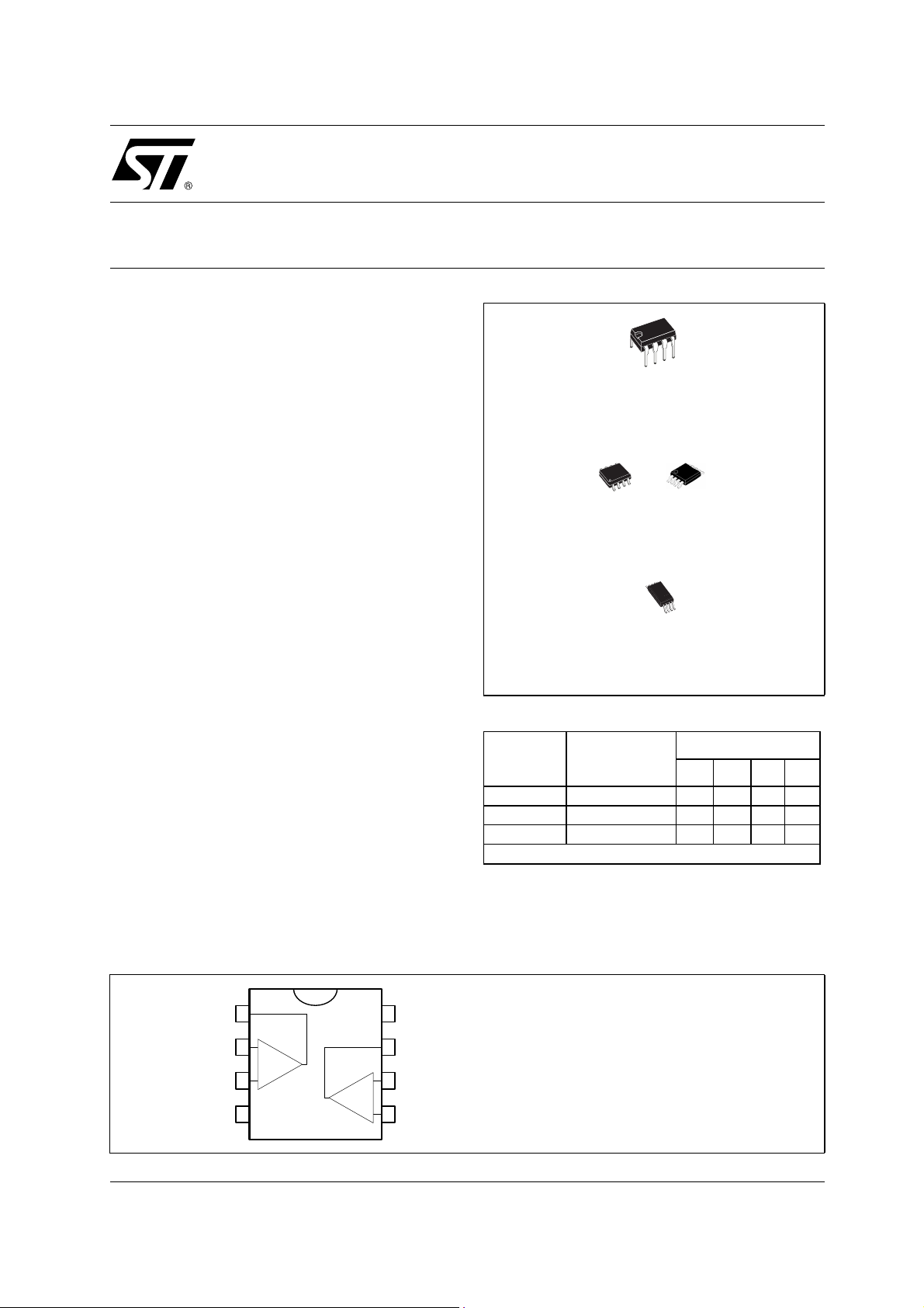
N
DIP8
(Plastic Package)
D & S
SO8 & miniSO8
(Plastic Micropackage)
P
TSSOP8
(Thin Shrink Small Outline Package)
ORDER CODE
Part
Number
LM158,A -55°C, +125°C
LM258,A -40°C, +105°C
LM358,A 0°C, +70°C
Example : LM258N
N = Dual in Line Package (DIP)
D = Small Outline Package (SO) - also available in Tape & Reel (DT)
S = Small Outline Package (miniSO) only available in Tape & Reel (DT)
P = Thin Shrink Small Outline Package (TSSOP) - only available in Tape
&Reel (PT)
Temperature
Range
Package
NSDP
•••
•••
••••
PIN CONNECTIONS (top view)
July 2003
1 - Output 1
2 - Inverting input
3 - Non-inverting input
-
4 - V
CC
5 - Non-inverting input 2
6 - Inverting input 2
7 - Output 2
8 - V
CC
+
1/12
Page 2
LM158,A-LM258,A-LM358,A
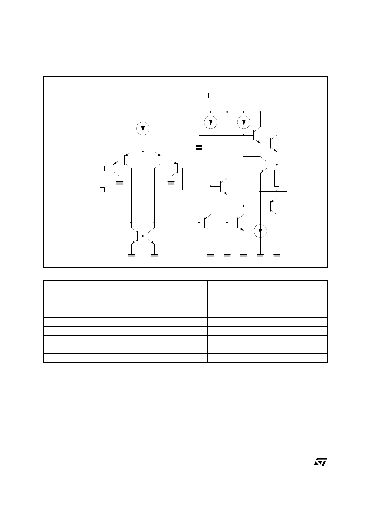
SCHEMATIC DIAGRAM (1/2 LM158)
V
CC
Inverting
input
Non-inverting
input
Q2
6µA
Q3
Q4Q1
4µA
C
C
100µA
Q5
Q6
Q7
R
SC
Q11
Output
Q13
Q10
Q12
Q8 Q9
50µA
GND
ABSOLUTE MAXIMUM RATINGS
Symbol Parameter LM158,A LM258,A LM358,A Unit
V
P
T
T
1. Power dissipation must be considered to ensure maximum junction temperature (Tj) is not exceeded.
2. Short-circuits from the output to VCC can cause excessive heating if VCC > 15V. The maximum output curr ent is approximately 40mA independent
3. This input current only exists when the voltage at any of the input leads is driven negative. It is due to the collector-base junction of the input PNP
Supply voltage +/-16 or 32 V
CC
V
Input Voltage -0.3 to +32 V
i
V
Differential Input Voltage +32 V
id
Power Dissipation
tot
Output Short-circuit Duration
I
Input Current
in
Opearting Free-air Temperature Range -55 to +125 -40 to +105 0 to +70 °C
oper
Storage Temperature Range -65 to +150 °C
stg
of the magnitude of V
transistor becoming forward biased and ther eby acti ng as input diodes clamps. In additi on to t his diode acti on, ther e is also NPN parasitic act ion on
the IC chip. this transistor action can cause the output voltages of the Op-amps to go to the V
for the time duration than an input is driven negative.
This is not destructive and normal output will set up again for input voltage higher than -0.3V.
CC
1)
2)
3)
. Destructive dissipation can result from simultaneous short-circuit on all amplifiers.
CC
500 mW
Infinite
50 mA
voltage level (or to ground for a large overdrive)
2/12
Page 3
LM158,A-LM258,A-LM358,A
ELECTRICAL CHARACTERISTICS
+
= +5V, V
V
CC
Symbol Parameter
Input Offset Voltage - note 1)
V
io
Input Offset Current
I
io
Input Bias Current - note
I
ib
Large Signal Voltage Gain
A
vd
Supply Voltage Rejection Ratio (R
SVR
I
CC
Input Common Mode Voltage Range
V
icm
Common Mode Rejection Ratio (R
CMR
I
Output Current Source
source
Output Sink Current (Vid = -1V)
I
sink
Output Voltage Swing ( RL = 2k
V
OPP
-
= Ground, Vo = 1.4V, T
CC
= +25°C
T
amb
LM158, LM258
LM158A
T
≤ T
min
amb
≤ T
max
LM158, LM258
= +25°C
T
amb
T
≤ T
≤ T
amb
max
= +25°C
≤ T
≤ T
amb
max
= +15V, RL = 2k
= +25°C
≤ T
≤ T
amb
+
= 5V to 30V
max
= +25°C
≤ T
≤ T
amb
max
2)
Vo = 1.4V to 11.4V
Ω,
T
T
V
T
T
V
T
T
min
amb
min
CC
amb
min
CC
amb
min
Supply Current, all Amp, no load
T
≤ T
≤ T
min
amb
≤ T
min
amb
= +30V - note
CC
= +25°C
≤ T
amb
≤ T
min
= +25°C
≤ T
min
CC
CC
CC
amb
min
≤ T
amb
= +15V, Vo = +2V, Vid = +1V
= +15V, Vo = +2V
= +15V, Vo = +0.2V
= +25°C
≤ T
≤ T
amb
V
T
T
T
T
V
T
amb
amb
V
V
T
T
VCC = +5V
max
≤ T
VCC = +30V
max
3)
max
max
max
= +25°C (unless otherwise specified)
amb
LM158A-LM258A
LM358A
Min. Typ. Max. Min. Typ. Max.
13
2
4
210
30
20 50
100
5025100 5025100
≤ 10kΩ)
s
6565100 6565100
0.7 1.2
1
+
-1.5
V
CC
+
V
CC
≤ 10kΩ)
s
0
0
706085 706085 dB
20 40 60 20 40 60
101220
50
Ω)
0
0
+
-1.5
V
CC
+
V
CC
-2
-2
LM158-LM258
LM358
27
23040nA
20 150
0.7 1.2
0
0
101220
50
0
0
V
CC
V
CC
V
CC
V
CC
5
9
7
200
2
+
-1.5
+
-2
+
-1.5
+
-2
Unit
mV
nA
V/mV
dB
mA
V
mA
mA
A
µ
3/12
Page 4
LM158,A-LM258,A-LM358,A
Symbol Parameter
LM158A-LM258A
LM358A
LM158-LM258
LM358
Unit
Min. Typ. Max. Min. T yp. Max.
High Level Output Voltage (V
T
= +25°C RL = 2k
V
OH
amb
≤ T
T
min
T
T
amb
= +25°C RL = 10k
amb
≤ T
min
amb
≤ T
≤ T
max
max
CC
+
= 30V)
Ω
Ω
26
26
27
27
27
28
26
26
27
27
27
28
V
Low Level Output Voltage (RL = 10kΩ)
V
OL
T
T
amb
min
= +25°C
≤ T
amb
≤ T
max
520
20
52020mV
Slew Rate
= 15V, Vi = 0.5 to 3V, RL = 2kΩ,
SR
V
CC
C
= 100pF, unity Gain 0.3 0.6 0.3 0.6
L
V/µs
Gain Bandwidth Product
= 30V, f =100kHz,Vin = 10mV, RL = 2kΩ,
GBP
V
CC
C
= 100pF 0.7 1.1 0.7 1.1
L
MHz
Total Harmonic Distortion
THD
e
n
DV
DI
Iio
V
o1/Vo2
1. Vo = 1.4V, Rs = 0Ω, 5V < V
2. The direction of the input current is out of the IC. This current is essentially constant, independent of the state of the output so no loading change
exists on the input lines.
3. The input common-mode voltage of either input signal voltage should not be allowed to go negative by more than 0.3V. The upper end of the
common-mode voltage range is V
4. Due to the proximity of external components insur e that co upling i s not orig inati ng via str ay capaci tance between these ex ternal parts. This typically
can be detected as this type of capacitance increases at higher frequences.
f = 1kHz, A
C
= 100pF, VO = 2Vpp
L
Equivalent Input Noise Voltage
f = 1kHz, R
Input Offset Voltage Drift 7 15 7 30
io
Input Offset Current Drift 10 200 10 300 pA/°C
Channel Separation - note 4)
1kHz ≤ f ≤ 20kHZ
= 20dB, RL = 2k
v
= 100Ω, VCC = 30V
s
+
< 30V, 0 < Vic < V
CC
+
- 1.5V, but either or both inputs can go to +32V without damage.
CC
Ω,
CC
Vo = 2V
+
- 1.5V
,
pp
0.02 0.02
55 55
120 120
nV
----------- -
V/°C
µ
%
Hz
dB
OPEN LOOP FREQUENCY RESPONSE
140
amb
V
I
+125°C
0.1mF
120
100
80
60
40
VOLTAGE GAIN (dB)
20
VCC = +10 to + 15V &
T
-55°C
0
1.0 10 100 1k 10k 100k 1M 10M
FREQUENCY (Hz)
4/12
-
VCC/2
+
VCC = 30V &
T
-55°C
amb
10M
W
V
CC
+125°C
(NOTE 3)
V
O
LARGE SIGNAL FREQUENCY RESPONSE
20
15
10
5
OUTPUT SWING (Vpp)
0
1k 10k 100k 1M
V
I
FREQUENCY (Hz)
1k
+7V
100k
W
W
+15V
-
+
VO
2k
W
Page 5

LM158,A-LM258,A-LM358,A
(mA)
VOLAGE FOLLOWER PULSE RESPONSE
4
RL 2 k
W
3
VCC = +15V
2
OUTPUT
1
VOLTAGE (V)
0
3
2
1
INPUT
010203040
VOLTAGE (V)
TIME (ms)
VOLTAGE FOLLOWER PULSSE RESPONSE
500
450
400
350
OUTPUT VOLTAGE (mV)
300
250
0 1 2 3 4 5 6 7 8
(SMALL SIGNAL)
+
e
-
l
Output
e
O
50pF
Input
T
amb
VCC= 30 V
= +25°C
TIME (ms)
OUTPUT CHARACTERISTICS
10
1
0.1
OUTPUT VOLTAGE (V)
0.01
0,001 0,01 0,1 1 10 100
VCC = +5V
VCC = +15V
VCC = +30V
vcc/2
v
cc
-
+
T
= +25°C
amb
OUTPUT SINK CURRENT
OUTPUT CHARACTERISTICS
8
7
VCC/2
6
(V)
5
+
CC
4
Independent of V
TO V
3
T
2
OUTPUT VOLTAGE REFERENCED
1
amb
0,01 0,1 1 10 100
0,001
+
-
= +25°C
V
CC
V
O
I
O
CC
OUTPUT SOURCE CURRENT (mA)
I
O
V
O
INPUT CURRENT (Note 1)
90
80
VI = 0 V
70
60
VCC = +30 V
50
40
VCC = +15 V
30
20
INPUT CURRENT (mA)
VCC = +5 V
10
0
-55 -35 -15 5 25 45 65 85 105 125
TEMPERATURE (°C)
CURRENT LIMITING (Note 1)
90
80
-
70
60
+
50
40
30
20
OUTPUT CURRENT (mA)
10
0
-55 -35 -15 5 25 45 65 85 105 125
TEMPERATURE (°C)
I
O
5/12
Page 6

LM158,A-LM258,A-LM358,A
0
)
0
(°C)
INPUT VOLTAGE RANGE
15
10
5
Négative
Positive
INPUT VOLTAGE (V)
0 5 10 15
POWER SUPPLY VOLTAGE (±V)
160
R = 20k
L
120
80
40
VOLTAGE GAIN (dB)
R = 2k
SUPPLY CURRENT
4
V
CC
I
D
mA
3
-
2
+
T
= 0°C to +125°C
1
amb
SUPPLY CURRENT (mA)
T
= -55°C
amb
0102030
POSITIVE SUPPLY VOLTAGE (V)
100
W
75
W
L
50
25
INPUT CURRENT (nA)
T = +25°C
amb
0 10 20 30 4
POSITIVE SUPPLY VOLTAGE (V
160
R = 20k
L
120
R = 2k
80
40
VOLTAGE GAIN (dB)
L
0 10 20 30
POSITIVE SUPPLY VOLTAGE (V)
0 10 20 3
POSITIVE SUPPLY VOLTAGE (V)
1.5
W
1.35
1.2
1.05
W
0.9
0.75
V = 15V
CC
0.6
0.45
0.3
0.15
0
GAIN BANDWIDTH PRODUCT (MHz)
-55-35-15 5 25 45 65 85 105 125
TEMPERATURE
6/12
Page 7

LM158,A-LM258,A-LM358,A
115
110
105
SVR
100
95
90
85
80
75
70
65
-55-35-15 5 25 45 65 85 105 125
60
POWER SUPPLY REJECTION RATIO (dB)
TEMPERATURE (°C)
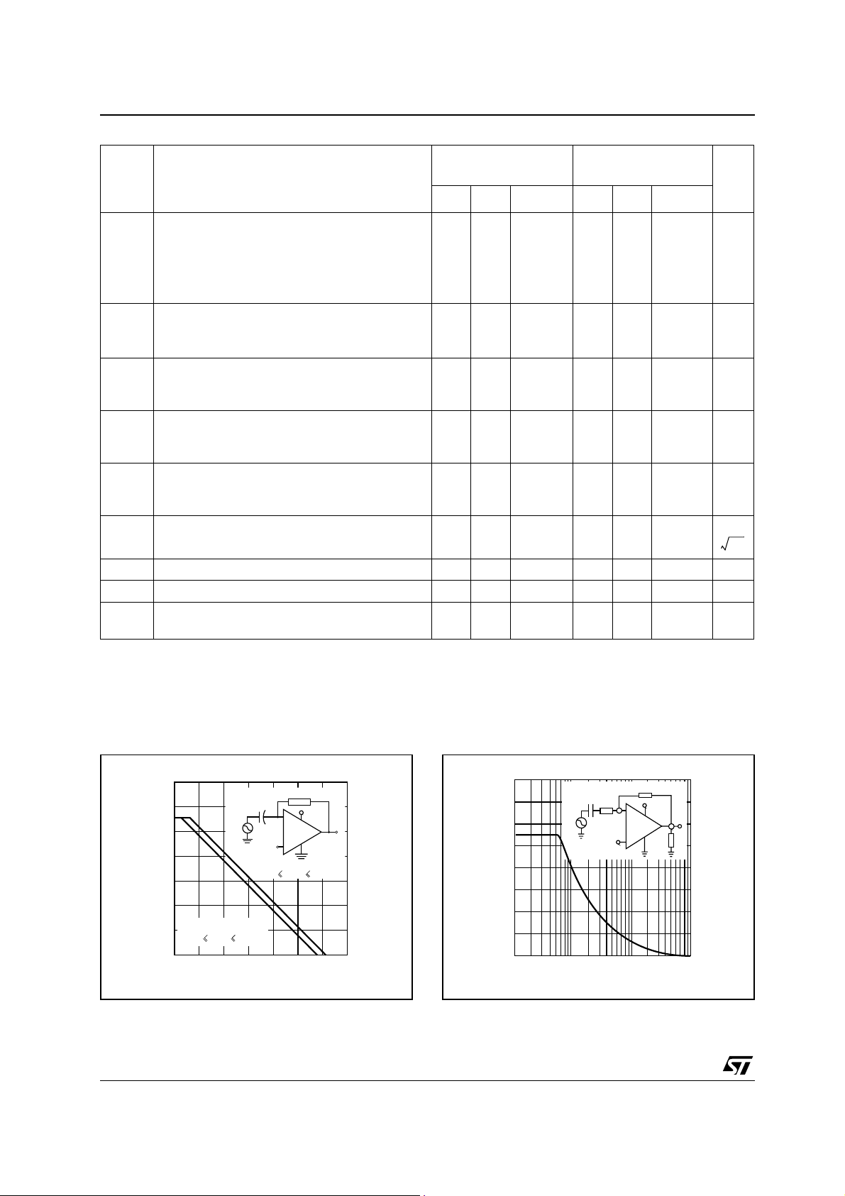
TYPICAL APPLICA T IO NS (si ngle supply voltage) V
AC COUPLED INVERTING AMPLIFIER
R
f
W
100k
R1
C
W
10k
I
1/2
LM158
R
B
6.2k
e
I
R2
~
W
100k
V
CC
C1
10mF
100k
W
R3
W
R
f
A=-
V
R1
(as shown A =-10)
V
C
o
0
e
o
R
L
10k
W
2V
PP
115
110
105
100
95
90
85
80
75
70
65
-55-35-15 5 25 45 65 85 105 125
60
= +5V
cc
COMMON MODE REJECTION RATIO (dB)
dc
TEMPERATURE (°C)
AC COUPLED NON-INVERTING AMPLIFIER
C1
0.1mF
R1
100k
C
I
e
I
~
1M
10mF
R2
1M
W
R3
W
C2
1/2
LM158
6.2k
100k
100k
W
R
B
W
R4
W
R5
W
A
=1+
V
(as shown A = 11)
C
o
V
CC
R2
R1
V
0
e
o
R
L
10k
W
2V
PP
NON-INVERTING DC AMPLIFIER
A
=1+
V
(As shown = 101)
e
O
+5V
(V)
O
e
0
e
10k
W
10k
1/2
LM158
R2
W
R1
W
1M
I
R2
R1
(mV)
DC SUMMING AMPLIFIER
e
W
100k
1
A
V
e
W
100k
2
e
W
100k
3
e
100k
W
4
eo = e1 + e2 - e3 - e
where (e1 + e2) ≥ (e3 + e4)
to keep e
≥
o
4
0V
100k
1/2
W
LM158
100k
e
O
W
7/12
Page 8

LM158,A-LM258,A-LM358,A
HIGH INPUT Z, DC DIFFERENTIAL AMPLIFIER
R2
100k
1/2
LM158
W
R1
100k
W
+V1
+V2
if R1 = R5 and R3 = R4 = R6 = R7
e
= [ 1 + ] ( (e2 + e1)
o
As shown e
R
2
-----------
R
2
= 101 (e
o
1
+ e1)
2
R3
100k
W
R4
100k
1/2
LM158
W
V
o
HIGH INPUT Z ADJUSTABLE GAIN DC
INSTRUMENTATI O N AMP L IFIER
R1
100k
W
R3
1/2
R
1
2
-----------
R
2
= 101 (e
o
LM158
Gain adjust
LM158
100k
1/2
e
1
R2
W
2k
e
2
if R1 = R5 and R3 = R4 = R6 = R7
e
= [ 1 + ] ( (e2 + e1)
o
As show n e
100k
R5
W
R6
100k
+ e1)
2
R4
100k
W
W
1/2
LM158
R7
100k
W
e
O
W
USING SYMMETRICAL AMPL IFIERS TO
REDUCE INPUT CURRENT
e
1.5M
1/2
LM158
I
I
B
I
I
I
B
2N 929
0.001mF
I
3M
B
1/2
W
LM158
I
B
I
B
W
e
o
Input current compensation
LOW DRIFT PEAK DETECTOR
I
B
1/2
LM158
I
C
2I
2N 929
B
B
0.001mF
I
B
3R
W
3M
I
B
Z
o
1/2
LM158
Input current
compensation
1/2
LM158
e
I
Z
I
1mF
1M
2I
B
R
W
e
o
ACTIVE BAND-PAS S FILTER
R2
100k
100k
R3
W
W
+V1
8/12
100k
1/2
LM158
R4
10M
R1
LM158
W
W
C2
330pF
1/2
R6
470k
W
R8
100k
C1
330pF
R5
W
470k
1/2
LM158
V
R7
100k
C3
m
10
W
F
o
W
V
CC
Page 9

PACKAGE MECHANICAL DATA
8 PINS - PLASTIC DIP
LM158,A-LM258,A-LM358,A
Dim.
Min. Typ. Max. Min. Typ. Max.
A 3.32 0.131
a1 0.51 0.020
B 1.15 1.65 0.045 0.065
b 0.356 0.55 0.014 0.022
b1 0.204 0.304 0.008 0.012
D 10.92 0.430
E 7.95 9.75 0.313 0.384
e 2.54 0.100
e3 7.62 0.300
e4 7.62 0.300
F 6.6 0260
i 5.08 0.200
L 3.18 3.81 0.125 0.150
Z 1.52 0.060
Millimeters Inches
9/12
Page 10

LM158,A-LM258,A-LM358,A
PACKAGE MECHANICAL DATA
8 PINS - PLASTIC MICROPACKAGE ( miniSO )
0,25 mm
c
E1
A2
A1
.010 inch
GAGE PLANE
SEATING
5
PLANE
k
L
L1
C
EA
4
D
b
C
ccc
PIN 1 IDENTIFICATION
8
e
1
Dim. Millimeters Inches
Min. Typ. Max. Min. Typ. Max.
A 1.100 0.043
A1 0.050 0.100 0.150 0.002 0.004 0.006
A2 0.780 0.860 0.940 0.031 0.034 0.037
b 0.250 0.330 0.400 0.010 0.013 0.016
c 0.130 0.180 0.230 0.005 0.007 0.009
D 2.900 3.000 3.100 0.114 0.118 0.122
E 4.750 4.900 5.050 0.187 0.193 0.199
E1 2.900 3.000 3.100 0.114 0.118 0.122
e 0.650 0.026
L 0.400 0.550 0.700 0.016 0.022 0.028
L1 0.950 0.037
k 0d3d6d0d3d6d
ccc 0.100 0.004
10/12
Page 11

PACKAGE MECHANICAL DATA
8 PINS - PLASTIC MICROPACKAGE (SO)
LM158,A-LM258,A-LM358,A
L
A
a2
b
e3
D
8
1
M
5
4
s
F
c1
C
E
a3
a1
b1
Millimeters Inches
Dim.
Min. Typ. Max. Min. Typ. Max.
A 1.75 0.069
a1 0.1 0.25 0.004 0.010
a2 1.65 0.065
a3 0.65 0.85 0.026 0.033
b 0.35 0.48 0.014 0.019
b1 0.19 0.25 0.007 0.010
C 0.25 0.5 0.010 0.020
c1 45° (typ.)
D 4.8 5.0 0.189 0.197
E 5.8 6.2 0.228 0.244
e 1.27 0.050
e3 3.81 0.150
F 3.8 4.0 0.150 0.157
L 0.4 1.27 0.016 0.050
M 0.6 0.024
S 8° (max.)
11/12
Page 12

LM158,A-LM258,A-LM358,A
PACKAGE MECHANICAL DATA
8 PINS - THIN SHRINK SMALL OUTL INE PAC KAGE (TSSOP)
k
c
E1
0.25mm
.010 inch
GAGE PLANE
SEATING
PLANE
L
L
C
L1
L1
A
A2
A1
5
D
b
PIN 1 IDENTIFICATION
5
8
8
E
4
e
1
14
Millimeters Inches
Dim.
Min. Typ. Max. Min. Typ. Max.
A 1.20 0.05
A1 0.05 0.15 0.01 0.006
A2 0.80 1.00 1.05 0.031 0.039 0.041
b 0.19 0.30 0.007 0.15
c 0.09 0.20 0.003 0.012
D 2.90 3.00 3.10 0.114 0.118 0.122
E 6.40 0.252
E1 4.30 4.40 4.50 0.169 0.173 0.177
e 0.65 0.025
k 0° 8° 0° 8°
l 0.50 0.60 0.75 0.09 0.0236 0.030
L 0.45 0.600 0.75 0.018 0.024 0.030
L1 1.000 0.039
Information furnished is bel ieved to be accurate and reliable. However, STMicroe lectronics assumes no responsibility for the
consequences of use of such information nor for any infringement of patents or other rights of third parties which may result from
its use. No li cense is granted by imp lication or otherwise under any patent or patent rig hts of STMicroelectronics. Specifications
mentioned in this publication ar e subject to change without notice. This publication supersedes and replaces all information
previously supplied. S TMicroelectronics products are not authorized for use as critica l components in life suppo rt devices or
systems without express written approval of STMicroelectronics.
The ST logo is a registered trademark of STMicroelectronics
© 2003 STMicroelectronics - All Rights Reserved
STMicr o el ectronics GROUP OF COMPANIES
Australi a - Brazil - China - Finland - France - Germany - Hong Kong - India - Italy - Japan - Malaysi a - Malta - Morocco
Singapo re - Spain - Swe den - Switzerl and - United K i ngdom
http://www.st.com
12/12
 Loading...