

Page 1
1
2.5V Low-Voltage Adjustable
Precision Shunt Regulator
NIKO-SEM
L431
JAN-08-Y02
GENERAL DESCRIPTION
The L431 is a three-terminal adjustable shunt
regulator utilizing an accurate 2.5V band-gap
reference. The output voltage can be set to any
value between 2.5V (V
REF
) to 29V with two
external resistors as shown in the typical
application circuit. The device exhibit a wide
operating current range of 0.4 to 100 mA with a
typical dynamic impedance of 0.25Ω. The cha-
racteristics of these reference make it excellent replacements for zener diodes in many
applications such as digital voltmeters, power
supplies, and op amp circuitry. The 2.5V volt
reference makes it convenient to obtain a
stable reference from 5.0V logic supplies.
The L431 shunt regulator is available in three
voltage tolerances (0.5%, 1.0% and 2%) and
three package options (TO-92, SOT-23-3,
SOT-23-5 and SOIC-8).
FEATURES
z Internal amplifier with 70 mA capability
z Programmable output voltage to 29V
z 0.25Ωtypical output impedance
z Pin to pin compatible with TL431, LM431
, SC431 & AS431
z Trimmed band-gap design 0.5%, 1.0%
and 2% with three package options
z Low cost solution
APPLICATIONS
z Linear regulator controller
z Precision voltage reference
z Switching power supplies
z Battery operating equipment
z Instrumentation
z PCs, Computer disk drives
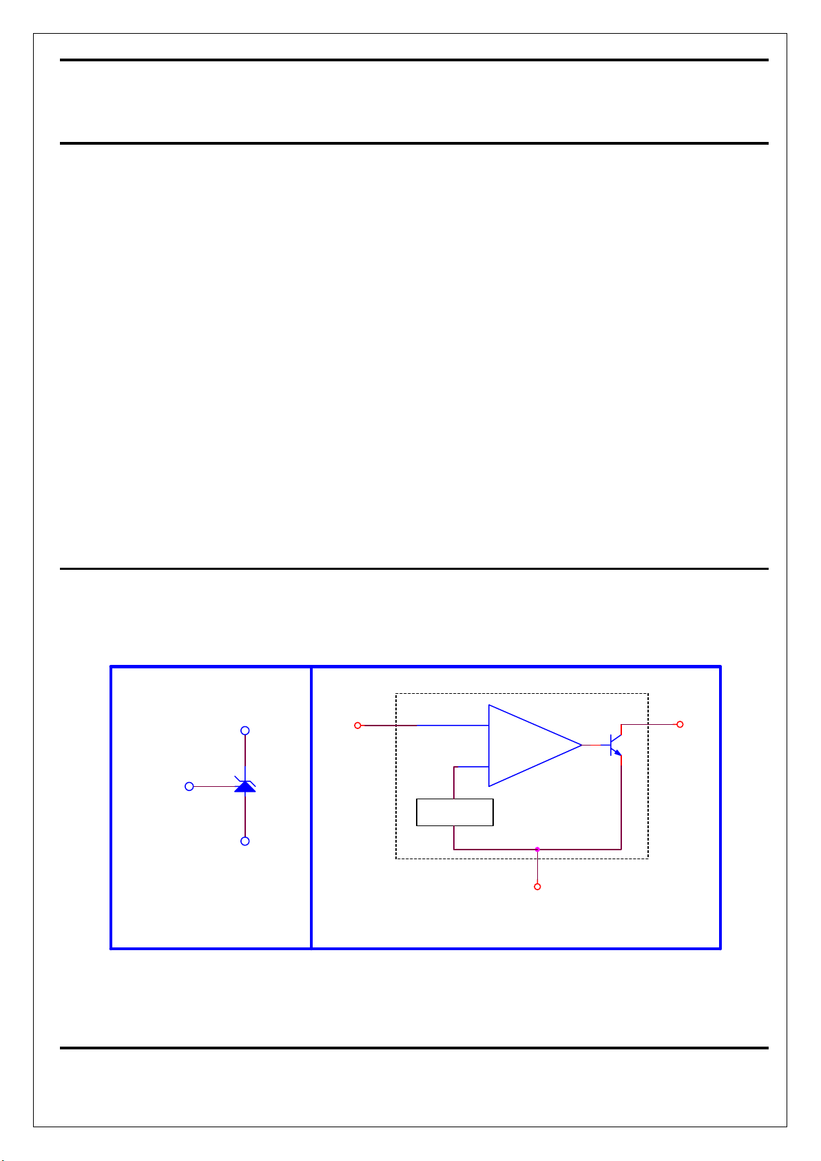
SYMBOL & BLOCK DIAGRAM
Anode (A)
Cathod
Reference
-
+
Cathode (K)
Anode (A)
Reference (R)
2.5 Vref
FUNCTIONAL BLOCK DIAGRAM
SYMBOL
(R) (K)
Page 2
2
2.5V Low-Voltage Adjustable
Precision Shunt Regulator
NIKO-SEM
L431
JAN-08-Y02
ABSOLUTE MAXIMUM RATINGS
PARAMETER VALUE
Cathode-Anode Reverse Breakdown Voltage - VKA 30V
Anode-Cathode Forward Current - IAK 70 mA
Reference Input Current - I
REF
10 mA
Storage Temperature Range - T
STG
-65 to +150 °C
Junction Temperature - TJ 150 °C
Lead Temperature (Soldering, 10 Seconds) - TL 300 °C
Continuous Power at 25 °C - P
D
TO-92
SOIC-8
SOT-23
700 mW
650 mW
200 mW
RECOMMENDED CONDITIONS TYPICAL THERMAL RESISTANCES
Parameter Rating Package
θJA θJC
Typ. Derating
Cathode Voltage (VKA) V
REF
to 29V TO-92 160 °C/W 80 °C/W 6.3 mW/°C
Cathode Current (IK) 10 mA SOIC-8 175 °C/W 45 °C/W 5.7 mW/°C
SOT-23 575 °C/W 150 °C/W 1.7 mW/°C
ELECTRICAL SPECIFICATIONS
(Ambient temperature must be derated base on power dissipation and package thermal characteristics. The conditions are: VKA = V
REF
and
I
K
= 10 mA unless otherwise stated)
PARAMETER TEST CONDITIONS MIN TYP MAX
UNITS
TEST
CIRCUIT
TA = 25 °C, L431 (0.5%) 2.482 2.495 2.507
TA = 25 °C, L431 (1%) 2.470 2.495 2.520
Reference Voltage
TA = 25 °C, L431 (2%) 2.445 2.495 2.550
V
1
∆V
REF
with Temp. 0.07 0.2
mV/°C
1
V
REF
to 10V -2.7 -1.0 Ration of Change in V
REF
to
Cathode Voltage
10V to 30V -2.0 -0.4 0.3
mV/V
2
Reference Input Current 0.7 4
µA
2
I
REF
Temp. Deviation Over Temp. 0.4 1.2
µA
2
Min. IK for Regulation 0.4 1
mA
1
Off State Leakage V
REF
= 0V, VKA = 30V 0.04 250
nA
3
Dynamic Output Impedance
f ≤ 1KHz, IK = 1 to 70 mA
0.25 0.5
Ω
1
Page 3
3
2.5V Low-Voltage Adjustable
Precision Shunt Regulator
NIKO-SEM
L431
JAN-08-Y02
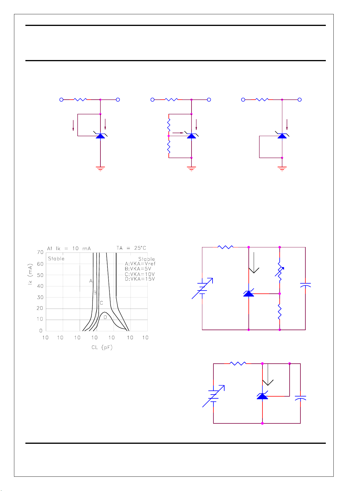
TEST CIRCUITS
IN
VV
KA
K
I
REF
I
V
REF
R1
R2
- TEST CIRCUIT 2 >(V
KA
V
REF
)
REF
I
)V
KA
V
=
- TEST CIRCUIT 1 -
KA
V
REF
(V
IN
- TEST CIRCUIT 3 -
KA
VV
IN
K (OFF)
I
(OFF STATE CURRENT)
I
K
The areas under the curves represent conditions that may
cause the device to oscillate. For curves B, C and D, R
1 and
V
BATT were adjusted to establish the initial VKA and IKA
conditions with C
L = 0. VBATT and CL then were adjusted
to determine the ranges of stability.
Stability Boundary Condition For Shunt Regulation
VS. Cathode Current and Load Capacitance
1023 4 56
CL
Ik
150
12
L431
2 3
1
Test Circuit for Vka = Vref
150
L431
2 3
1
10K
R2
Test Circuit for Vka > Vref
Ik
R1
CLVBATT
12
Page 4
4
2.5V Low-Voltage Adjustable
Precision Shunt Regulator
NIKO-SEM
L431
JAN-08-Y02
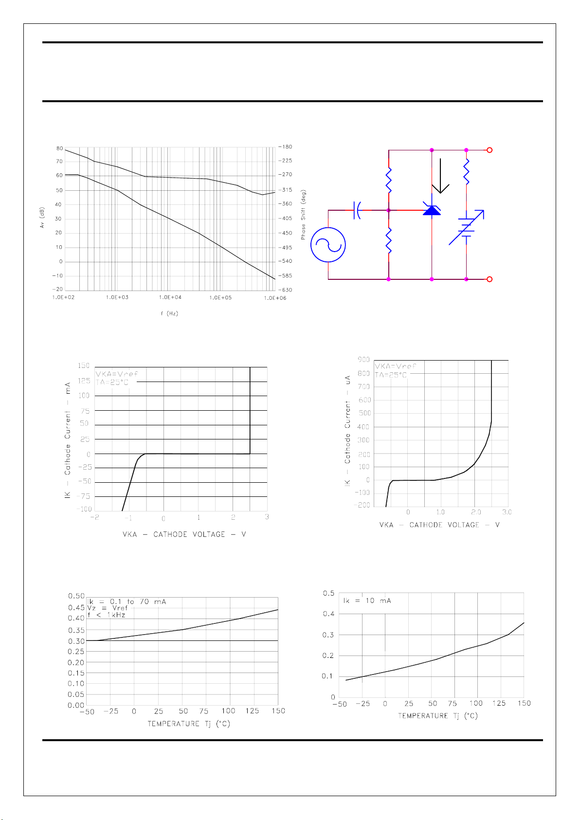
Small-Signal Gain and Phase Shift
VS. Frequency
VS. Cathode Voltage
Cathode Current
Cathode Current
VS. Cathode Voltage
VS. Junction Temperature
r
z
(
Ω
)
Reference Impedance
VS. Junction Temperature
Ratio of Delta Reference Voltage to Delta Cathode Voltage
Δ
V
r
e
f
/
Δ
V
z
(
-
m
V
/
V
)
ΔVz = 3V to 30V
8.25K
OUT
Ik
GND
15K
12
L431
2 3
1
10uF
232
12
Test Circuit for Small Signal Gain and Phas
e
Page 5

5
2.5V Low-Voltage Adjustable
Precision Shunt Regulator
NIKO-SEM
L431
JAN-08-Y02
VS. Junction Temperature
Off-State Cathode Current
VS. Junction Temperature
Reference Voltage
VS. Frequency
Reference Impedance
Ω
Reference Input Current
∞
VS. Junction Temperature
Page 6

6
2.5V Low-Voltage Adjustable
Precision Shunt Regulator
NIKO-SEM
L431
JAN-08-Y02
PIN CONFIGURATION
DEVICE SELECTION GUIDE
Device
L431NB L431M3B L431VB L431M5B
Package
TO-92 SOT-23-3 SOIC-8 SOT-23-5
Marking
L431N 1M3 L431V 1M5A
Tolerance
1% 1% 1% 1%
Page 7

7
2.5V Low-Voltage Adjustable
Precision Shunt Regulator
NIKO-SEM
L431
JAN-08-Y02
APPLICATION CIRCUIT
+
10uF
+
Cout
+
Cin
P01N02LM or P3055L
L431 or L432
R1
R2
1K
5V or 12V
Vin
Vout
G
D S
A
K R
Niko
Niko
Vout = (1 + ) Vref
R2
R1
Page 8

8
2.5V Low-Voltage Adjustable
Precision Shunt Regulator
NIKO-SEM
L431
JAN-08-Y02
TO-92 MECHANICAL DATA
mm mm
Dimension
Min. Typ. Max.
Dimension
Min. Typ. Max.
A 4.445 5.207 H 2.413 2.540 2.667
B 4.318 5.334 I 0.356 0.533
C 12.7 15.5 J
D 0.356 0.533 K
E 1.143 1.27 1.397 L
F 3.175 4.191 M
G 0.762 1.270 N
Page 9

9
2.5V Low-Voltage Adjustable
Precision Shunt Regulator
NIKO-SEM
L431
JAN-08-Y02
SOT-23 (M3) MECHANICAL DATA
mm mm
Dimension
Min. Typ. Max.
Dimension
Min. Typ. Max.
A 0.95 H 0.10 0.15 0.25
B 2.60 2.80 3.00 I 0.37
C 1.40 1.60 1.80 J
D 2.70 2.90 3.10 K
E 1.00 1.10 1.30 L
F 0.00 0.10 M
G 0.35 0.4 0.5 N
Page 10

10
2.5V Low-Voltage Adjustable
Precision Shunt Regulator
NIKO-SEM
L431
JAN-08-Y02
SOIC-8 (D) MECHANICAL DATA
mm mm
Dimension
Min. Typ. Max.
Dimension
Min. Typ. Max.
A 4.8 5.0 H 0.4 1.27
B 3.8 4.0 I 0.18 0.25
C 5.8 6.2 J 0.22
D 0.35 0.48 K
0°
8°
E 1.27 L
F 1.65 M
G 0.1 0.25 N
Page 11

11
2.5V Low-Voltage Adjustable
Precision Shunt Regulator
NIKO-SEM
L431
JAN-08-Y02
SOT-23 (M5) MECHANICAL DATA
mm mm
Dimension
Min. Typ. Max.
Dimension
Min. Typ. Max.
A 1.0 1.10 1.30 e 1.90(TYP)
A1 0.00 0.10 H 2.60 2.80 3.00
A2 0.70 0.80 0.90 L 0.37
b 0.35 0.40 0.50
C 0.10 0.15 0.25
D 2.70 2.90 3.10
E 1.40 1.60 1.80
 Loading...