

Page 1
VERY LOW DROP 5V REGULATOR WITH RESET
.PRECISEOUTPUT VOLTAGE(5 V ± 4%)
.VERYLOW DROPOUTVOLTAGE
.OUTPUTCURRENT INEXCESSOF 500mA
.POWER-ON, POWER-OFF INFORMATION
(RESET FUNCTION)
.HIGH NOISE IMMUNITY ON RESET DELAY
CAPACITOR
L387A
DESCRIPTION
The L387A is a very low drop voltage regulator in
a Pentawatt
vide stabilized 5V supplies in consumer and industrial applications. Thanks to its very low input/output voltage drop this device is very useful
in battery powered equipment, reducing consumption and prolonging battery life. A reset output makes the L387A particularly suitable for microprocessor systems. This output provides a reset signal when power is applied (after an external programmable delay) and goes low when
ABSOLUTE MAXIMUM RATINGS
Symbol Parameter Value Unit
T
j,Tstg
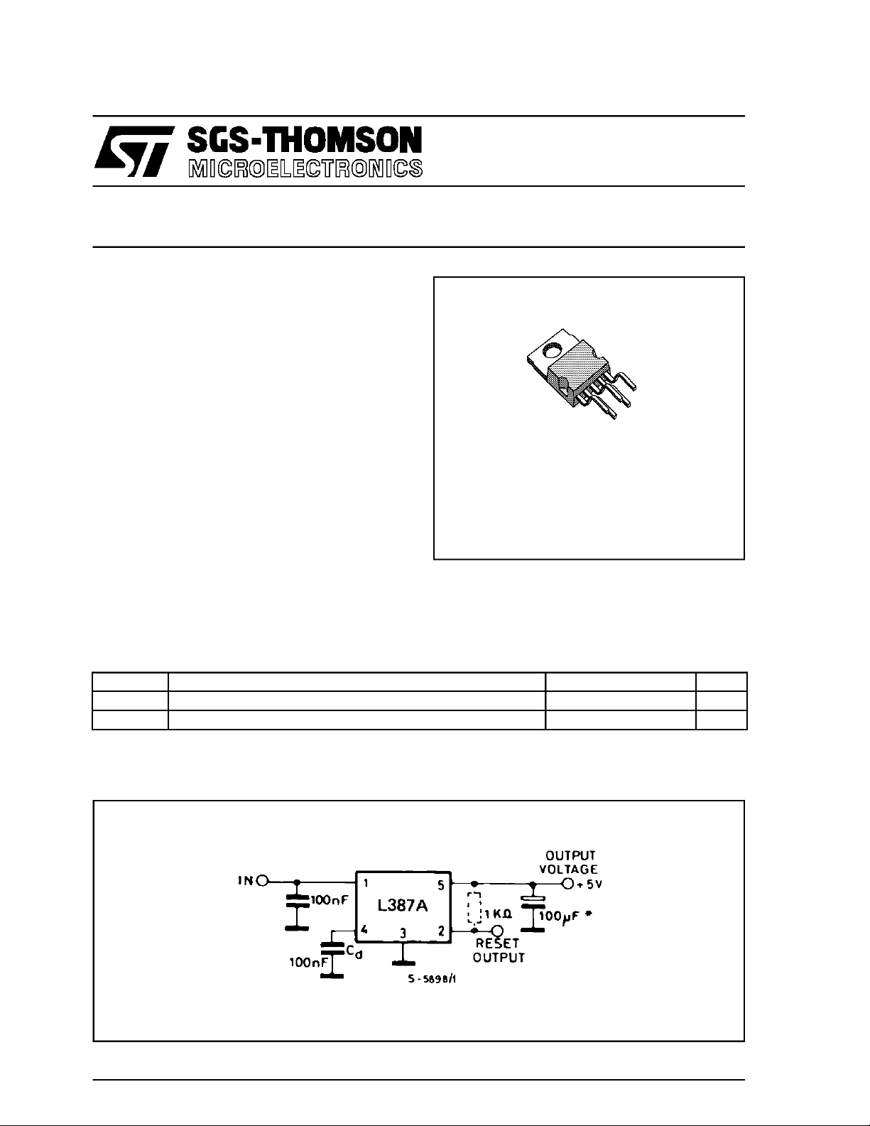
APPLICATION CIRCUIT
package specially designed to pro-
ORDERING NUMBER : L387A
power is removed, inhibiting the microprocessor.
An hysteresis on reset delay capacitor raises the
immunity to the ground noise.
V
D.C. Input Voltage 35 V
i
Junction and StorageTemperatureRange –55 to 150 °C
Pentawatt
* Min33 µF and max.ESR ≤ 3 Ω over temperaturerange.
October1991
1/6
Page 2
L387A
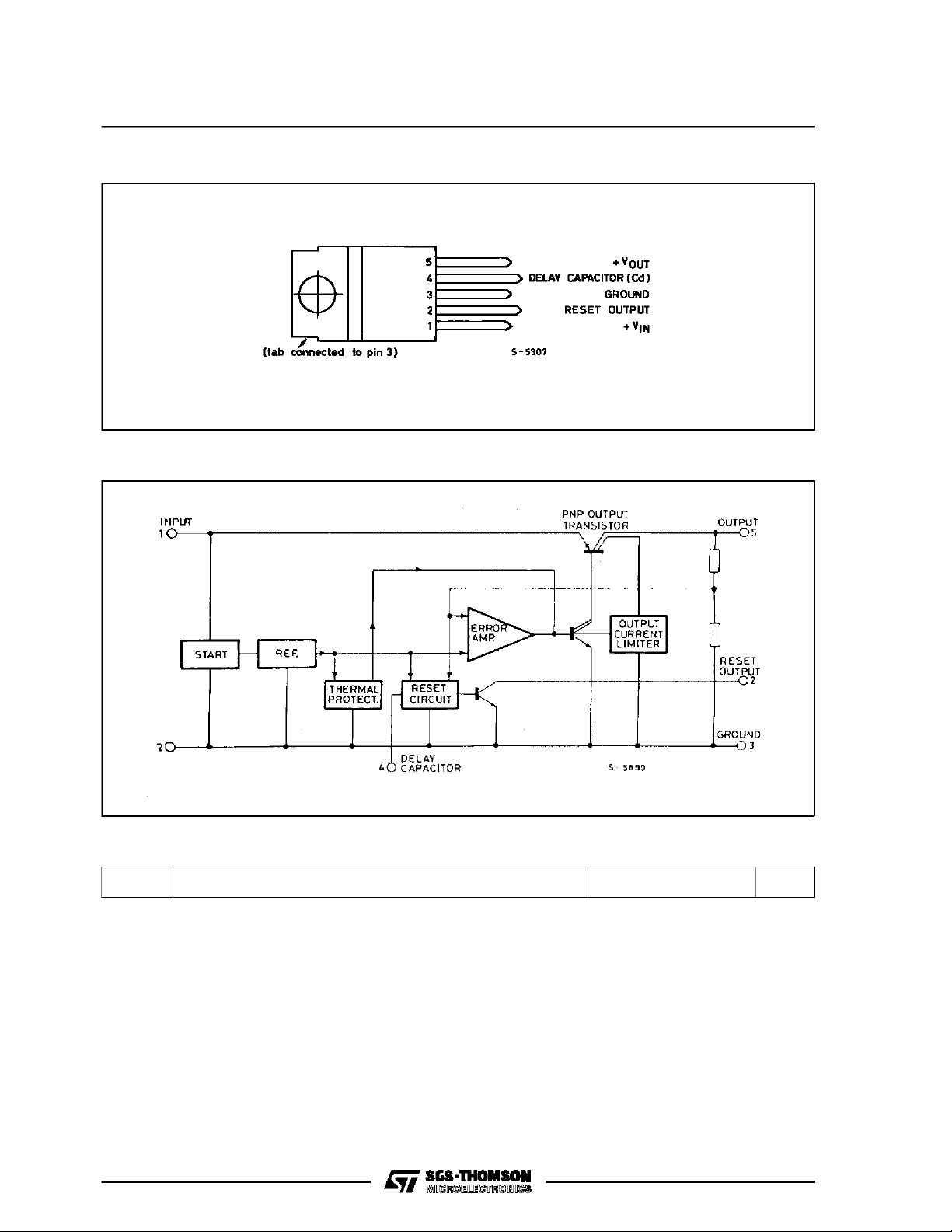
PIN CONNECTION (Top views)
BLOCK DIAGRAM
THERMAL DATA
R
2/6
t h j-ca se
Thermal Resistance Junction-case Max 4 °C/W
Page 3

L387A
ELECTRICAL CHARACTERISTICS (refer to the test circuit, Vi= 14.4 V, Tj=25°C, Co= 100 µF;
unless otherwisespecified)
Symbol Parameter Test Conditions Min. Typ. Max. Unit
Output Voltage Io= 5 mA to 500 mA Tj=25°C
V
o
Operating Input Voltage (*), Over Full T Range (– 40 to 125 °C)
V
I
–40≤T
≤125 °C
j
4.80
4.75
(see note **)
∆V
∆V
V
I–Vo
∆ V
∆ T
SVR Supply Voltage Rejection I
Line Regulation Vi=6Vto26V Io=5mA 5 50 mV
o
Load Regulation Io= 5 mA to 500 mA 15 60 mV
o
Dropout Voltage VO=V
= 350 mA
I
o
= 500 mA
I
o
Quiescent Current Io=0mA
I
q
= 6.2 V Io= 500 mA 160 180 mA
V
i
Temperature Output
o
O NOM
– 100 mV
= 150 mA
I
o
I
= 350 mA
o
= 500 mA
I
o
Voltage Drift
= 350 mA f = 120 Hz
o
Output Short Circuit
I
SC
= 100 µFV
C
o
=12V±5V
i
pp
Current
Reset Output Voltage IR= 3 mA 1 < Vo< 4.70 V
V
V
RT (off)
R
Reset Output Leakage
I
R
Current
Delay Time for Reset
t
d
Output
I
= 16 mA 1.5 < Vo< 4.75 V
R
Over Full T (– 40 °C ≤ T
≤ 125 °C)
j
Voin Regulation VR=5V
Over Full T Range
Cd = 100 nF
Over Full T Range
Vo@ Reset out H to L Transition, Over
4.75 V
Full T Range
Charging Current
I
C4
V4=3V 102030µA
(current generator)
V
RT (on)
Power on
V
Threshold
o
Comparator Threshold
V
4
(pin 4)
Hysteresis Voltage Over Full T Range 450 mV
V
H
(*) For a DC volt age 26 < Vi < 37 V the d evic e is not operating.
(**) Design lim i ts are guaranteed (but not 100 % production tested) over the indicated t emperat ure and supply voltage ranges.
These limits are not used to calculate outgoing quality levels.
@ Reset out L to H Transition , Over
V
o
Full T Range
V4@ Reset out H to L Transition 3.2 3.9 V
@ Reset out L to H Transition 3.7 4.3 V
V
4
5.00
5.00
5.20
5.25
26 V
0.40
0.60
20
60
100
0.65
0.8
5
15
35
100
160
mA
mA
mA
mA
– 0.5 mV/°C
60
1.2 1.6 A
0.5
0.8
50 µA
25 ms
o
– 0.15
V
RT (off)
+0.05V
V
o
–0.04V
V
V
V
V
V
V
V
V
3/6
Page 4

L387A
Figure 1 : Dropout Voltage vs. Output Current.
Figure 3 : OutputVoltage vs. Temperature.
Figure 2 : Quiescent Current vs. Output
Current.
4/6
Page 5

PENTAWATT PACKAGE MECHANICAL DATA
L387A
DIM.
MIN. TYP. MAX. MIN. TYP. MAX.
mm inch
A 4.8 0.189
C 1.37 0.054
D 2.4 2.8 0.094 0.110
D1 1.2 1.35 0.047 0.053
E 0.35 0.55 0.014 0.022
F 0.8 1.05 0.031 0.041
F1 1 1.4 0.039 0.055
G 3.4 0.126 0.134 0.142
G1 6.8 0.260 0.268 0.276
H2 10.4 0.409
H3 10.05 10.4 0.396 0.409
L 17.85 0.703
L1 15.75 0.620
L2 21.4 0.843
L3 22.5 0.886
L5 2.6 3 0.102 0.118
L6 15.1 15.8 0.594 0.622
L7 6 6.6 0.236 0.260
M 4.5 0.177
M1 4 0.157
Dia 3.65 3.85 0.144 0.152
A
H3
L
L1
C
D1
Dia.
L7
L6
D
L2
L3L5
F1
H2
E
MM1
G1
G
F
5/6
Page 6

L387A
Information furnished is believed to be accurate and reliable. However, SGS-THOMSON Microelectronics assumes no responsibility for
the consequences of use of such information nor for any infringement of patents or other rights of third parties which may result from its
use. No license is granted by implication or otherwise under any patent or patent rights of SGS-THOMSON Microelectronics. Specifications mentioned in this publication are subject to change without notice. This publication supersedes and replaces all information previously supplied. SGS-THOMSON Microelectronics products are not authorized for use as critical components in life support devices or
systems without express written approval of SGS-THOMSON Microelectronics.
PENTAWATT
Australia - Brazil - France - Germany - Hong Kong - Italy - Japan - Korea - Malaysia - Malta - Morocco - The Netherlands - Singapore -
Spain - Sweden - Switzerland - Taiwan - Thaliand - United Kingdom - U.S.A.
1994 SGS-THOMSON Microelectronics - All Rights Reserved
is registered trademarks of SGS-THOMSON Microelectronics
SGS-THOMSON Microelectronics GROUP OF COMPANIES
6/6
 Loading...