

Page 1

PRELIMINARY
ENHANCED CALLING LINE IDENTIFIER WITH CALL WAITING KS8630D
BRIEF DESCRIPTION
16-SOP-225
KS8630D is a Low power mixed signal CMOS integrated circuit
for receiving a physical layer signals used in the Calling Line
Identification Presentation (CLIP) of British Telecom system,
the Calling Identity Delivery(CID) of Bellcore system, and
similar evolving systems before the call is put through. It can
also satisfy the requirements of CIDCW (Calling Identity
Delivery on Call Waiting) services including very high precision
detection of CAS (CPE Alerting Signal) tone and the signals
used in similar services when the call has already been put
through.
KS8630D carries out the following features : Ring or Line-reversal detection, CAS ( 2130Hz and 2750Hz) Tone
detection, and 1200-baud FSK demodulation which simultanesouly satisfies the BELL202 and the CCITT ( ITU-T )
V.23 specification. The demodulated data for Caller Identification is transmitted serially to the related u-controller.
KS8630D using a patented digital algorithm to detect demodulated FSK signals and CAS signal detection.
The device also has a built-in Automatic Gain Control circuitry which is capable of very high precision detection of
CAS tone. It is suitable for use in Adjunct Boxes or Feature Phones with CID / CIDCW applications.
FEATURES
• CID and CIDCW System Operation
• High Performance CAS Detection and Loop State Tone Alert signal detection
• Internal Automatic Gain Control circuitry for the high precision CAS detection
• Digital Logic FSK demodulator
• Ring or Line-polarity reversal detection
• Low power consumption in standby mode
• 3.58MHz crystal oscillator
• 3.3V ~ 5V Operation
• 16-SOP package ( 225Mil )
APPLICATIONS
• CID / CIDCW Adjunct Boxes and Feature Phones
• A system for British Telecom, Bellcore, CCA
• Computer Telephone Integrated system
• Call Logging Systems
• Voice-Mail Equipment
ORDERING INFORMATION
Device Package Operating Temperature
KS8630 16-SOP-225 0°C ~ 70°C
1
Page 2
PRELIMINARY
RTB
XOUT
KS8630D ENHANCED CALLING LINE IDENTIFIER WITH CALL WAITING
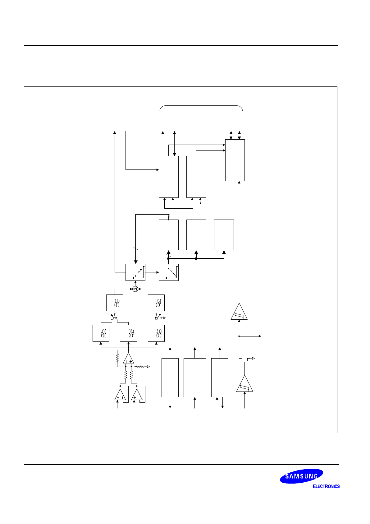
BLOCK DIAGRAM
TO/FROM MICROCONTROLLER
OFFHOOK
AGC_VB
5
AGC
DATA
DCLK
FSK
DEMODULATOR
GAIN
CONTROL
8
ADC
TONE
DISCRIMINATOR
PEAK
DETECTOR
MODE
MODE &
INTERRUPT
LEVEL
DETECTOR
INTB
GENERATOR
BPF
LPF
INN
BPF
INP
LPF
BPF
BIAS
GENERATOR
VREF
BLOCK
SENSING
VOLTAGE
PD
Figure 1. KS8630D Block Diagram
CLOCK GEN
OSCILLATOR &
XIN
RD
2
Page 3
PRELIMINARY
ENHANCED CALLING LINE IDENTIFIER WITH CALL WAITING KS8630D
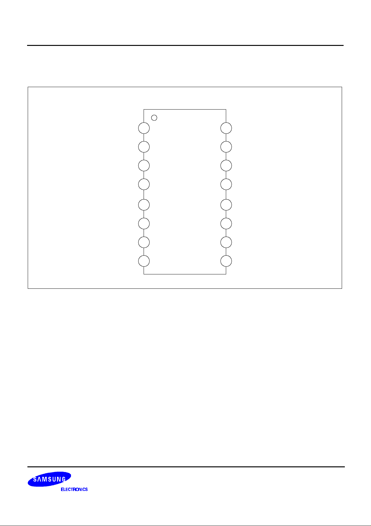
PIN DIAGRAM
V
DD
AGC_VB
I
NN
I
NP
V
REF
RD
RTB
PD
1
2
3
16
15
14
KS8630D
4
5
6
7
8
Figure 2. KS8630D Pin Diagram
13
12
11
10
9
XOUT
XIN
INTB
DCLK
OFFHOOK
MODE
DATA
V
SS
3
Page 4

PRELIMINARY
KS8630D ENHANCED CALLING LINE IDENTIFIER WITH CALL WAITING
PIN DESCRIPTION
Pin No. Pin Name Type Description
1 V
DD
P Positive Power Supply.
2 AGC_VB O AGC block bias terminal. Usually a 0.47uF capacitor is connected between this
3 I
4 I
5 V
NN
NP
REF
pin and V
I Inverting input of the on-chip input signal amplifier.
I Non-inverting input of the on-chip input signal amplifier.
O Reference Voltage. Typically 0.1 ~ 1uF is connected to GND.
pin to reduce a dc offset produced by internal circuitry.
REF
6 RD I(S) Schmitt trigger input to detect the ringing signal, ring-burst signal, Line-polarity
reversal signal.
7 RTB I(S)/O Open drain output/Schmitt trigger input.
An external resistor to V
and a capacitor to VSS should be connected with
DD
RTB to filter and to extend the RD input signal. Each components value is
related to the schmitt trigger input threshold and input signal frequency.
8 PD I(S) Power Down. Schmitt trigger & voltage sensing input.
If set to high level, all circuitry goes to power down mode except ring detection
& mode selection block. In order to satisfy the BT or Bellcore specification, it is
recommended to add a different application circuits.
All digital block can be resetted by this pin control. Whenever the u-controller
unmutes handset and enables keypad in Off-Hook state, KS8630D must
receive a reset pulse by this pin from microcontroller.
9 V
SS
P Negative Power Supply.
10 DATA B Demodulated FSK data output. Default state is a logic high level.
DATA is tranmitted serially to the microcontroller ( 8bit /unit, LSB first ).
DCLK is used for sync clock of this DATA.
In case of using this pin as input, it is used for testing of KS8630D functionality.
11 MODE B Mode output signal to show the current status ( Ring / Dual Tone / FSK signal
receiving). Default state is a logic high level.
If detects a CAS tone, this MODE pin will be set to logic low level during a pre-
determined timming. If detects a Ring or FSK signal, this pin will be set to high
level. With the INTB pin, it can be informed current status to microcontroller.
In case of using this pin as input, it is used for testing of KS8630D functionality.
12 OFFHOOK I Hook Status Input. If set to high level, the operation condition of KS8630D go
to the Off-Hook state. If set to low level, it goes to the On-Hook state.
13 DCLK B Synchronous clock output of DATA. Default state is logic high level.
The right data is in falling edge of this clock. In case of using this pin as input,
it is used for testing of KS8630D functionality
4
Page 5

PRELIMINARY
ENHANCED CALLING LINE IDENTIFIER WITH CALL WAITING KS8630D
PIN DESCRIPTION (Continued)
Pin No. Pin Name Type Description
14 INTB O Interrupt output signal. It is an active low output that may be used as an
Interrupt Request / Wake-up signal to the microcontroller.
In case of ringing or line polarity reversal detection, dual tone detection and the
mark signal detection of FSK data, it will be activated.
With the MODE pin, it indicates current status to the microcontroller.
15 XIN I The input of the 3.58MHz on-chip crystal oscillator inverter.
16 XOUT O The output to the 3.58MHz on-chip crystal oscillator inverter.
NOTES:
I = Input
I(S) = Schmitt trigger Input
O = Output
B = Bidirectional I/O
5
Page 6
PRELIMINARY
TO/FROM MICROCONTROLLER
KS8630D ENHANCED CALLING LINE IDENTIFIER WITH CALL WAITING
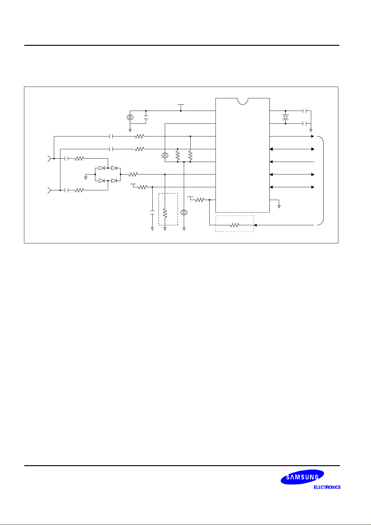
TYPICAL APPLICATION CIRCUIT
VDD
16
15
14
13
12
11
10
9
XOUT
XIN
INTB
DCLK
OFFHOOK
MODE
DATA
VSS
C1
X1
C2
TIP
RING
C7
C8
R1
R2
D3
D4
C3
C4
D1
D2
VDD
R3
R5
R6
C10
R4
C9
VDD
1
C6C5
R10
R7
AGC_VB
VDD
R8
VREF
R9
INN
INP
RD
RTB
PD
2
3
4
5
6
7
8
KS8630D
Note 1
C11
Note 2
R11
Figure 3. Recommended Typical Application Circuit Components
R1, R2, R3 470kΩ C1, C2 10pF
R4 150kΩ C3, C4 22nF
R5, R6, R7, R8 100kΩ C5 10µF
R9 82kΩ C6, C7, C8 100nF
R10 56kΩ C9 0.47µF
(Note 1) C10 220nF
R11 47kΩ
C11 0.1µF
(Note 2.)
X1 3.579545MHz
D1, D2, D3, D4 1N4004
NOTES:
1. When applying to the BT system, change R10 to 330kΩ to detect the Line Reversal signal.
2. When applying to the BT system, insert a resistance between the MCU’s PD related pin and KS8630D PD pin
(Refer to Section 1.6).
6
Page 7

PRELIMINARY
ENHANCED CALLING LINE IDENTIFIER WITH CALL WAITING KS8630D
GENERAL DESCRIPTION
KS8630D is suitable for use in both system to British Telecom specificatios and BELLCORE specifications.
KS8630D to be used in different systems, the predetermined signals must be applied to the PD (pin#8) and the
OFFHOOK ( pin#12), which are defined by the application circuits or the microcontroller.
All detection modes related to the PD pin and the OFFHOOK pin are listed below:
PD OFFHOOK DETECTION MODE (Note1) REMARK
L L FSK Demodulation BELLCORE
L H Dual Tone Detection →
FSK Demodulation
SYSTEM
(Note2)
1/3 * V
1/3 * V
DD
DD
L Dual Tone Detection →
FSK Demodulation
H Dual Tone Detection →
BT SYSTEM
(Note3)
FSK Demodulation
H L Ringing or Line reversal Detection
H H −
Table 1. A Status of each detection mode
NOTES:
1. If a false reponse (talk-off) occurs or microcontroller receives FSK data, microcontroller should send low edge pulse
(with 10us duration timming approximately) to the PD pin.
Then, KS8630D will be re-initialized to the dual tone(CAS) detection mode.
2. If KS8630D is used in the BELLCORE system, a pull-up resistor should be inserted between the PD pin and VDD.
3. If KS8630D is used in the BT system, a pull-up resistor should be inserted between the PD pin and VDD.
In this case, a resistor should be inserted between KS8630D’s PD pin and microcontroller’s PD related pin.
Then, the voltage level of KS8630D’s PD pin will be 1/3*VDD when microcontroller's PD related pin set to low state.
7
Page 8

PRELIMINARY
KS8630D ENHANCED CALLING LINE IDENTIFIER WITH CALL WAITING
FUNCTIONAL DESCRIPTION
Ring or Line Reversal Detector
It can be detected the Ringing signal or the Line polarity reversal signal as in the CLIP, CID, and CDS protocols.
The signals between Tip and Ring block pass through the bridge circuitry and the rectified signal is input to the
RD (pin #6). If the rectified signal is larger than the internal threshold VTH, the RTB block stays in the low level
while the signal is maintained by the external resistor and capacitor . For the Line polarity reversal detection,
the logic low level section within RTB block is also decided by the external resistor and capacitor value.
When a Ringing or a Line polarity reversal signal is detected, an active low pulse is outputted by the interrupt
generator to the INTB (pin#14) .
TIP
RING
C7
C8
TIP/RING
R1
R2
D3
D4
RD
KS8630
D1
R3
D2
R10
RD
VDD
RTB
R4 C10
Figure 4. Ring or Line Reversal Detector
INTERRUPT
GENERATOR
V
TH
vss
INTB
RTB
V
TH
vss
INTB
Figure 5. Signals of Ring Detection
8
Page 9

PRELIMINARY
ENHANCED CALLING LINE IDENTIFIER WITH CALL WAITING KS8630D
TIP/RING
RTB
INTB
Figure 6. Signals of Line Reversal Detection
V
TH
9
Page 10

PRELIMINARY
KS8630D ENHANCED CALLING LINE IDENTIFIER WITH CALL WAITING
Input Signal Amplifier
KS8630D can adjust the input signals appearing at the TIP/RING block in application, so that they are included
within the range that can be handled with the block. The internal Amp. configuration of KS8630D is a subtract
structure, and it was recommend that the signal input in the differential mode to the chip is reduced by half level
compared to the signal in the TIP/RING block.
C3
C4
C1
R5
R6
R2
INN
R
INP
R
VREF
R
R
Amplifier
(a)
INN
R
INP
R
R8R7
VREF
R
R
Amplifier
(b)
Figure 7. Input Signal Amplifier. (a) single-ended (b) differential-ended
Filtering Block
The outband noise of input signal which interfered by transmission line or Near-end speech is eliminated by the
filtering block. The filtering block includes the SCF-configured Dual Tone BPF, FSK BPF, and LPF for filtering the
SCF clock-generated noise. The dual tone BPF is a narrowband 4th filter which composed of biquads. The quality
factor of dual tone filter is between 20 and 25 approximately. The low tone filter and high tone filter are composed
of same core, and the cutoff frequency can be changed according to the switching clock (CLK1, CLK2).
The FSK BPF is a wideband 4th filter, and the Dual Tone BPF and FSK BPF can be selected according to the
detection mode in KS8630D .
10
Page 11

PRELIMINARY
ENHANCED CALLING LINE IDENTIFIER WITH CALL WAITING KS8630D
BPF
Volt[Lin]
-10
-20
-30
LPF
Output
Signal
LPF
Input
Signal
CLK1
BPF
CLK1
BPF
CLK2
Figure 8. Filtering Block
0
Volt[Lin]
0
-10
-20
-30
-40
-50
0 1K 2K 3K 4K 5K
Freq[Hz]
(a) (b)
Volt[Lin]
0
-5
-10
-15
-20
-25
-30
100 10k
Figure 9. BPF Characteristics
(a) low tone filter (b) high tone filter (c) FSK filter
1k
(c)
-40
-50
0 1K 2K 3K 4K 5K
Freq[Hz]
Freq[Hz]
11
Page 12

PRELIMINARY
KS8630D ENHANCED CALLING LINE IDENTIFIER WITH CALL WAITING
Automatic Gain Control
This block controls the AGC amplifier gain using the ADC output signal, so that the CAS detection and the FSK
demodulation block can be operated within an adequate dynamic range, and the ADC output can have enough
resolution. Connect a “Coff ” between AGC_VB and V
to eliminate the amplification of DC offset.
REF
AGC_VB
AGC
FILTER_OUT
5
COFF
VREF
ADC
8
GAIN
CONTROL
Figure 10. Automatic Gain Control Block
The range of input signals for AGC operation is about 35dB, and the gain of the input signal has an hysteresis
characteristics. If a signal which is larger than 7/8 of the ADC input dynamic range is input into the ADC, the gain
is immediately decreased. If a signal which is smaller than 1/4 of the ADC input dynamic range is continuously input
for more than a set amount of the time (about 2ms), the gain is immediately increased.
The ADC input dynamic range is about 2V.
12
Direction of Gain Decrease
Direction of Gain Increase
Figure 11. Figure 9. Input Signal vs. Gain
Page 13

PRELIMINARY
ENHANCED CALLING LINE IDENTIFIER WITH CALL WAITING KS8630D
Dual Tone Alerting Signal Detection (CAS signal detection)
The 2130Hz and 2750Hz components that are output from each BPF are synthesized, converted into AM
waveform, and used as the analog input to the 8-bit ADC. The synthesized analog signal is converted into digital
data through the ADC and in the given sampling rate. Use this data to find the highest peak (MXB) of the 2440Hz
component (frequency sum). Also, use this MXB to find the highest peak (PK) and lowest peak (BMN) of the 620Hz
component (frequency difference).
Carrier Signal : (2750 + 2130) / 2 = 2440Hz → Frequency Sum
Envelope Signal : (2750 - 2130) / 2 = 310Hz → Frequency Difference
Envelope Signal (310Hz)
Carrier Signal (2440Hz)
MXB
PK
BMN
Figure 12. ADC input signal waveform and calculated peak position
The PK error correction algorithm was applied in KS8630D to reduce the pseudo PK signal generation (from Voice
Noise) as much as possible. PK signals occur in a 620Hz period as shown in FIG 12. Since the PK occurs regularly
for a CAS signal, you can eliminate the pseudo PK using this characteristic. The corrected PK is used to carry out
the CAS detection algorithm.
First comes the CAS_SEEK block operation that checks whethere there is CAS within the channel. This block
uses the fact that MXB and PK signals occur within a specific range when CAS is being transmitted. After the CAS
signal has started the transmission, the gain control is carried out. While the ADC input is maintained at a specific
gain, it takes about 5ms to generate a CASIS signal.
The CAS detection algorithm is carried out immediately when CASIS becomes high.
It takes about 58ms after CASIS becomes high to detect any CAS.
13
Page 14

PRELIMINARY
KS8630D ENHANCED CALLING LINE IDENTIFIER WITH CALL WAITING
START
CAS_SEEK
block detects CAS like
signal(CASIS)?
Yes
CAS detection algorithm
is executed
58ms is elasped?
Yes
PRE_CAS is high?
Yes
LENGTH_CHK block is
executed
CASIS
falling edge goes
low ?
No
No
No
No
Yes
PRE_CAS's high
time is smalled than
22.5ms?
Yes
CAS is detected !!!
CAS is not detected !No
Figure 13. Dual Tone Alerting Signal(CAS) detection flowchart
1. Find the average value of the PK generation period from the envelope component, and check if it enters
into a specific margin.
2. Use AM waveform characteristics to check if the difference in the BMN level near PK exceeds specific
conditions.
3. Check if each PK’s interval is within specific conditions.
14
Page 15

PRELIMINARY
ENHANCED CALLING LINE IDENTIFIER WITH CALL WAITING KS8630D
About 58ms after the CASIS becomes high, check whethere all the above conditions are fulfilled, and if they are,
generate the PRE_CAS signal which signifies that there is CAS. If the PRE_CAS set to high as shown in FIG. 13,
the LENGTH_CHK block starts its operations. The pseudo CAS is rejected by using the fact that CAS’s off-hook
transmission is between 75ms ~ 85ms. If the PRE_CAS’s high duration is less than 22.5ms, CAS detection will be
carried out successfully.
KS8630D’s CAS detection uses the method of checking the sine wave’s characteristics while the ADC input gain is
regularly maintained, or uses the fact that the CAS signal’s transmission duration is always the same. Even when
CASIS becomes high, if the gain changes or it becomes known that it isn’t a different CAS, KS8630D comes out of
the CAS detection algorithm at once to prevent talk-off counting . Also, to prevent talk-down, we use an error
correction algorithm that restores the sine wave’s characteristics that have been distorted by Voice Noise, as much
as possible.
Line
Dual Tone Alert Signal
Signal
T
MODED
MODE
T
AMODE
T
MINT
INTB
T
INTD
Figure 14. Dual Tone Alerting Signal(CAS) detection timing
If CAS is detected after the CAS signal has started transmission and the algorithm of FIG 13. are all executed,
it should alert to the MCU using the MODE output and the INTB output. FIG 14. shows the timing of MODE and
INTB operation. After detecting that the CAS transmission is over, MODE after T
is enabled to low, and the
AMODE
INTB is sent to the MCU After this, the MCU expects FSK data from KS8630D and waits for it.
FSK Demodulation
KS8630D uses own digital FSK demodulation algorithm. The analog signal that has passed through the BPF which
has frequency band of FSK signal goes through the ADC and it is digitally converted in the specified sampling rate.
Same as the Dual Tone Alerting signal detection, the signal’s highest peak detecting algorithm is applied for finding
each frequency components’ peak. The interval information of the peaks are used to decide if the FSK data being
transmitted is mark bit(“1”) or space bit(“0”).
Although the Bellcore standards and BT’s FSK signal components are different, KS8630D raised circuit efficiency
by using an FSK demodulation algorithm that satisfies both standards in the same circuit.
When a Mark signal (normally, a continous mark bit(“1”) of minimum 58bits is transmitted) is found in the FSK data
being transmitted, the INTB signal is sent to MCU to tell it that the FSK data transmission will soon occur. When the
mark signal ends and caller information is sent starting at the start bit, it is sent to MCU through the DATA, DCLK
output.
15
Page 16

PRELIMINARY
KS8630D ENHANCED CALLING LINE IDENTIFIER WITH CALL WAITING
Line
Channel Seizure Mark signal FSK data
Signal
INTB
Figure 15. FSK demodulator operation timing (on-hook)
DATA Retiming
KS8630D uses two pins to send FSK data to MCU.
DATA sends the demodulated FSK data, and DCLK transmits the clock synchronous to DATA.
start bit start bit
Line
Signal
MARK signal
T
MKINT
"10101010" "10101010" "101"
b0b1b2b3b4b5b6b
7
stop bit stop bit
T
INTD2
Dummy Mark bit(n bit)
b0b1b2b3b4b5b6b
7
start bit
b0b1b
2
DATA
DCLK
T
DCLK
Figure 16. DATA and DCLK generation timing
16
Page 17

PRELIMINARY
ENHANCED CALLING LINE IDENTIFIER WITH CALL WAITING KS8630D
APPLICATION NOTES
ON-HOOK OPERATION
On-Hook means that the telephone set is not being used. In the On-Hook state, the caller ID information will be
displayed on the LCD pannel before you answer the call.
BT(British Telecom) system
In the On-Hook state, the BT protocol sends an “Idle State Tone Alerting Signal” by means of monitoring the input
signal level. For more detailed specification, please refer to British Telecom's SIN227, and SIN242.
Line Signal
RD
RTB
MODE
INTB
DATA
DCLK
PD
Line Reversal
100ms 88~110ms 45ms 80~262ms 45~72ms 2.5sec >200ms
Tone Alert
Channel
Seizure
MARK Message
Call Arrival Indication Signal
TMODED
AMODE
T
TINTD1
T
MINT
TINTD2
MKINT
T
TINTD2
data
clock
TINTPD
MSGPD
T
Ringing
Figure 17. British Telecom On-Hook System Signals
[1] : Sum of two periods may not exceed 5 sec.
[2] : Typically 500ms
[3] : please refer to FIG 16.
17
Page 18

PRELIMINARY
KS8630D ENHANCED CALLING LINE IDENTIFIER WITH CALL WAITING
The 2130Hz and 2750Hz components of the tone alert signal are transmitted simultaneously and the “10” is
continously repeated for the Channel seizure signal. The MARK signal is composed of continuous “1”, and the
message is consists of the start bit (“0”), 8-bit real data, stop bit (“1”) and inserted dummy Mark bit (0~20 bit).
A low edge pulse is generated into the INTB pin if KS8630D detects a Line polarity reversal.
Then the Microcontroller must detect this signal and put the PD pin into the Low State level.
Must be careful when the Microcontroller detects the end of FSK data or if the FSK data is not detected during the
set amount of time , so that the PD (pin # 8) of KS8630D becomes re-initialized back to Power Down Mode ( high
state).
Bellcore system
In the On-Hook state, the Bellcore protocol does not send the Dual Tone CPE Alerting Signal. For more detailed
information, please refer to Bellcore specification : GR-30-CORE, and SR-TSV-002476.
Max 2.9~3.7sec
Line Signal
Typically 2sec 250ms 150ms
1'st Ring
250~500ms 200ms
Channel
Seizure
MARK Message
2'nd Ring
RD
RTB
TMKINT
INTB
DATA
DCLK
PD
For the Channel seizure signal, the “10” is continously repeated. The MARK signal is composed of continuous “1”,
and the message is consists of the start bit (“0”), 8-bit data, stop bit (“1”) and inserted dummy Mark bit (0~20 bit).
TINTD1
TINTD2
data
clock
TINTPD TMSGPD
Figure 18. Bellcore On-Hook System Signals
When KS8630D detects the end of ringing signal, the INTB ( pin # 14) generates a low edge pulse.
The Microcontroller detects this signal and sets the PD( pin # 8) to low state level.
Must be careful when the Microcontroller detects the end of FSK data or if FSK data is not detected during the set
amount of time (approximately 500ms), so that that the KS8630D’s PD( pin # 8) becomes re-initialized back to
Power Down Mode (high state).
18
Page 19

PRELIMINARY
ENHANCED CALLING LINE IDENTIFIER WITH CALL WAITING KS8630D
OFF-HOOK OPERATION
Off-Hook means that the telephone set is currently being used. The CIDCW (Calling Identity on Call Waiting)
service means displaying a different Caller’s Identity on the LCD pannel while still on the line with another call.
Since the telephone set is being used, the operator must send a CAS (CPE Alerting Signal) before sending the
caller ID information, to initialize the CIDCW service. The performance of subscriber’s phone (CPE) is a error rate
of the CAS signal detection when the speech signal interfered as a noise. If talk-down (missing CAS) occurs, the
caller ID information can be lost, and if talk-off (false response) occurs, the caller at the far end will hear unwanted
noise. CAS is transmitted in the same frequency band as the voice signals, so that the talk-off and the talk-down
performance is very important to decide the efficiency of Caller ID system. KS8630D uses the BPF and patented
digital detection algorithm to detect the Dual Tone CPE Alerting Signal, so it is possible to minimize the talk-off
and the talk-down error ratio.
BT (British Telecom) system
NETWORK
Terminal
Equipment
MODE
INTB
DATA
DCLK
PD
Start
Point
40~50ms
Silence
Waiting for
ACK signal
80~85ms
Tone Alert MARK
Detect
Alert Signal
100ms
Disable
Speech path Send ACK
Detect
ACK signal
5~100ms
Silence
65~75ms
ACK
If no message detected,
restore speech path
TMODED
TAMODE
TMKINT
TINTD2 TINTD2
TMINT
45~75ms
Network Speech path
restored within 100ms
Message
data
clock
TMSGPD
PD
T
W
Figure 19. KS8630D's Timing Diagram in BT, Off-Hook Status
If the talk-off occurs, or if the microcontroller has finished transmitting FSK data, a high state pulse must be
transmitted to the PD ( pin # 8 ) to re-initialize the KS8630D same as FIG 19.
19
Page 20

PRELIMINARY
KS8630D ENHANCED CALLING LINE IDENTIFIER WITH CALL WAITING
Bellcore system
Off-Hook state data tranmission of Bellcore system is similar to the British Telecom system, but there is a
difference in timming.
CPE mute
handset
&disables
keypad
100ms
65~75ms
ACK
send ACK
5~100ms
CPE unmutes handset
& enables keypad
58~75ms 50ms
MARK
NETWORK
CPE
CPE goes
Off-Hook
75~85ms
CAS DATA
MODE
TAMODE
INTB
TMODED
TMKINT
TINTD2 TINTD2
TMINT
DATA
DCLK
PD
data
clock
T
TMSGPD
Figure 20. (d). KS8630D’s Timing Diagram in Bellcore, Off-Hook Status
If the talk-off occurs, or if the microcontroller has finished transmitting FSK data, a high state pulse must be
transmitted to the PD ( pin # 8 ) to re-initialize the KS8630D same as FIG 20.
PD
W
20
Page 21

PRELIMINARY
ENHANCED CALLING LINE IDENTIFIER WITH CALL WAITING KS8630D
ABSOLUTE MAXIMUM RATINGS (Ta = 25°C)
Characteristic Symbol Value Unit
Supply voltage V
Power Dissipation P
Operating Temperature T
Storage Temperature T
ELECTRICAL CHARACTERISTICS
(Ta = 25°C, VDD = 3.3V, unless otherwise specified)
Characteristics Symbol Min. Typ. Max. Unit
DC Characteristics
Operating Voltage V
Operating Current I
Schmitt Input High Threshold(RD) V
Schmitt Input Low Threshold(RD) V
Schmitt Input High Threshold(PD) V
Schmitt Input Low Threshold(PD) V
AC Electrical Characteristics
DD
DD
THR
TLR
THP
TLP
DD
D
OPR
STG
0.3 ~ 6.0 V
500 mW
0 ~ 70 °C
−65 ~ 150 °C
3.0 − 5.5 V
− − 5 mA
0.75*V
DD
− − 0.25*V
0.70*V
DD
− − 0.5*V
− − V
DD
− − V
DD
V
V
CAS, Idle State Alerting Tone Detection
Acceptance Range CAS
( ± 0.5%)
Rejection Range CAS
AR
RR
2120 2130 2140 Hz
2737 2750 2763 Hz
<2055 - >2205 Hz
<2653 - >2847 Hz
Acceptance Signal Level per tone CAS
Reject signal level per tone CAS
Positive and negative twist detect CAS
ASL
RSL
TD
-40 - -2 dBV
- - -46
[Note1]
- - 6 dB[Note2]
FSK detection
Transmission rate 1188 1200 1212 Baud
BELL202 MARK("1") 1188 1200 1212 Hz
BELL202 SPACE("0") 2178 2200 2222 Hz
V.23 MARK("1") 1280 1300 1320 Hz
V.23 SPACE("0") 2068 2100 2132 Hz
21
Page 22

PRELIMINARY
KS8630D ENHANCED CALLING LINE IDENTIFIER WITH CALL WAITING
ELECTRICAL CHARACTERISTICS (Continued)
(Ta = 25°C, VDD = 3.3V, unless otherwise specified)
Characteristics Symbol Min. Typ. Max. Unit
Input level detection FSK
Acceptable Twist Level FSK
Signal Timing Specification
CAS, Idle State Alerting Tone Detection
End of Tone Alert signal to MODE
T
AMODE
low timing
MODE low to INT low timing T
MODE low duration timing T
INT low duration timing when Ring /
MINT
MODED
T
INTD1
Line reversal occurs
INT low duration timing T
INTD2
FSK detection
MARK signal start time to INT low
T
MKINT
timing
DCLK's low duration time T
1st INTB to PD low time in On-Hook
state
DCLK
T
INTPD
[Note4]
LD
AT
-40.0 - -3.0 dBV
[Note3]
- - 6 dB
1.7 2.0 10 ms
200 250 300 us
15 18 20 ms
Same timing width as Ring / Line-reversal detection at
Tip / Ring. Refer to Fig 5 / Fig 6 Timing
1.5 1.7 2.0 ms
26 27 35 ms
60 70 80 us
1 5 10 ms
Message end to PD high time T
MSGPD
1 5 10 ms
[Note4]
PD high pulse width in Off-Hook state T
PDW
30 50 100 us
[Note4]
NOTES:
1. dBV: decibels above or below a reference voltage of 1 Vrms Signal level is per tone.
2. dB: Twist = 20 log (fH amplitude / fL amplitude)
3. dBV: decibels above or below a reference voltage of 1 Vrms.
cf) dBm : decibels above or below a reference power of 1mW into 600Ω.
0dBm = 0.7746Vrms.
4. These times are required by the Microcontroller.
For KS8630D to work properly, these timings must be observed.
22
Page 23

PRELIMINARY
L
ENHANCED CALLING LINE IDENTIFIER WITH CALL WAITING KS8630D
PACKAGE DIMENSION
DE
#9#16
#1 #8
G
H
I J K
A: 6.00 ± 0.30 / 0.236 ±0.012
B: 3.95 ±0.20 / 0.156 ±0.008
C: 5.72 / 0.225
D: 0 ~ 8°
E: 0.20 + 0.10, -0.05 / 0.008 + 0.004, - 0.002
F: 0.60 ±0.20 / 0.024 ±0.008
G: 10.30 MAX / 0.405 MAX
H: 9.90 / 0.390
I: 0.51 / 0.020
J: 0.41 ±0.10 / 0.016 ±0.004
K: 1.27 / 0.050
L: 0.05 MIN / 0.002 MIN
M: 1.55 ±0.20 / 0.061 ± 0.008
N: 1.95 MAX / 0.077 MAX
M
A
N
B
C
F
0.10 MAX
0.004 MAX
23
 Loading...